Used KLA / TENCOR P10 #293813796 for sale
URL successfully copied!
Tap to zoom
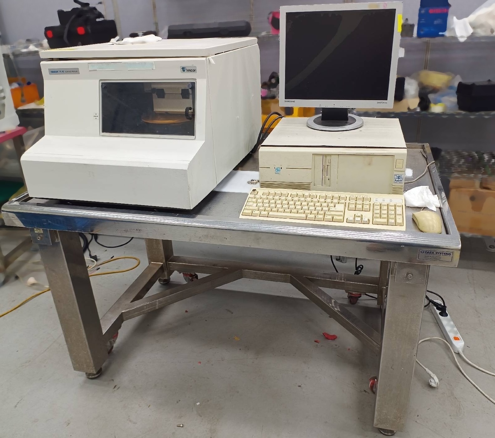

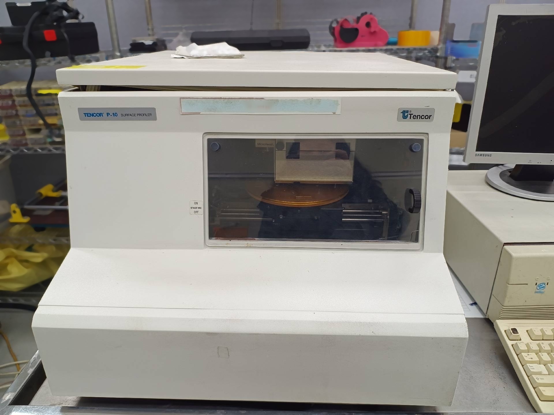
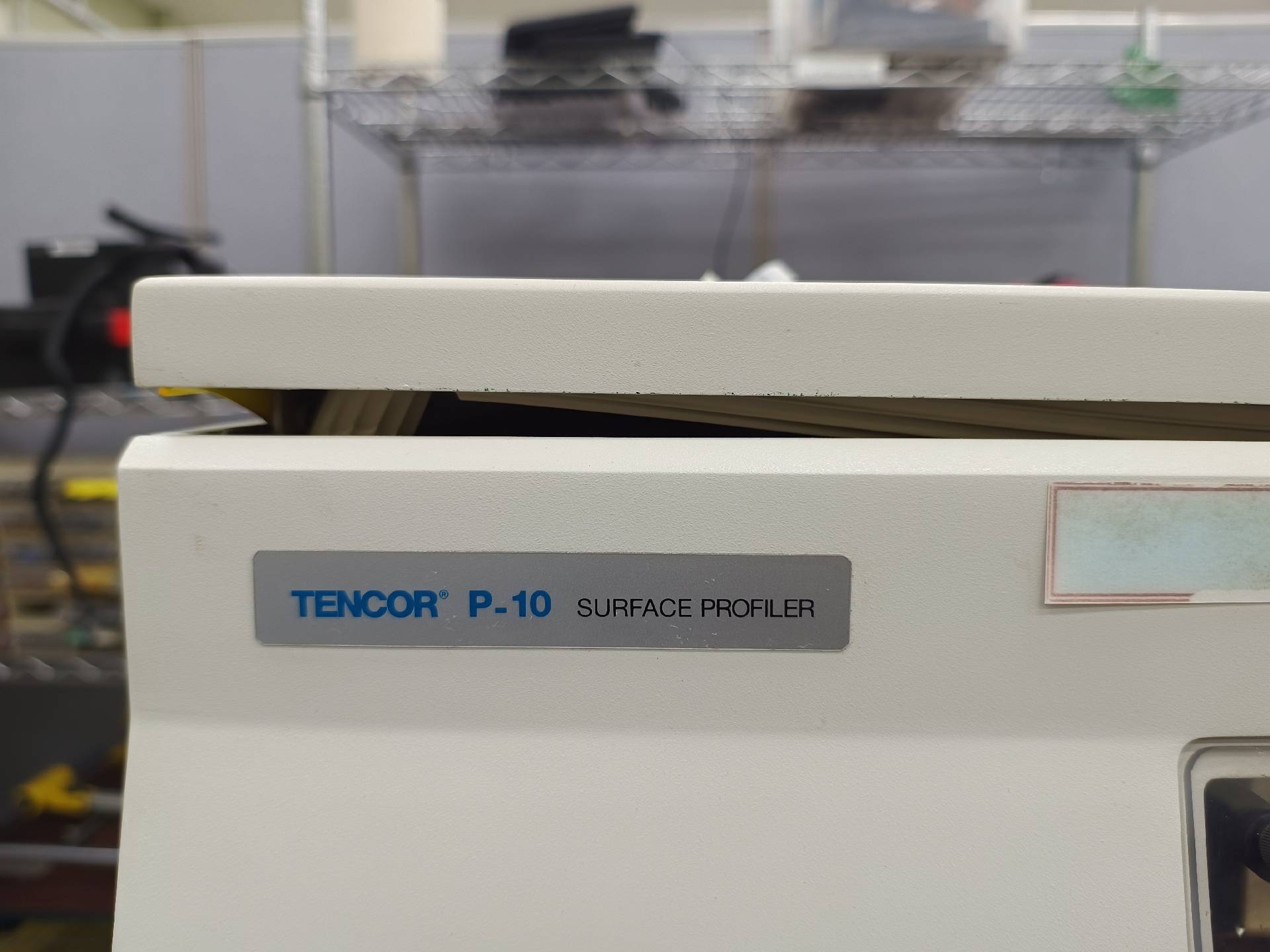
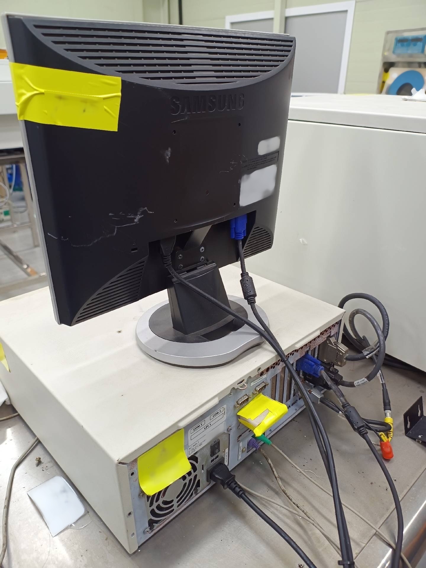
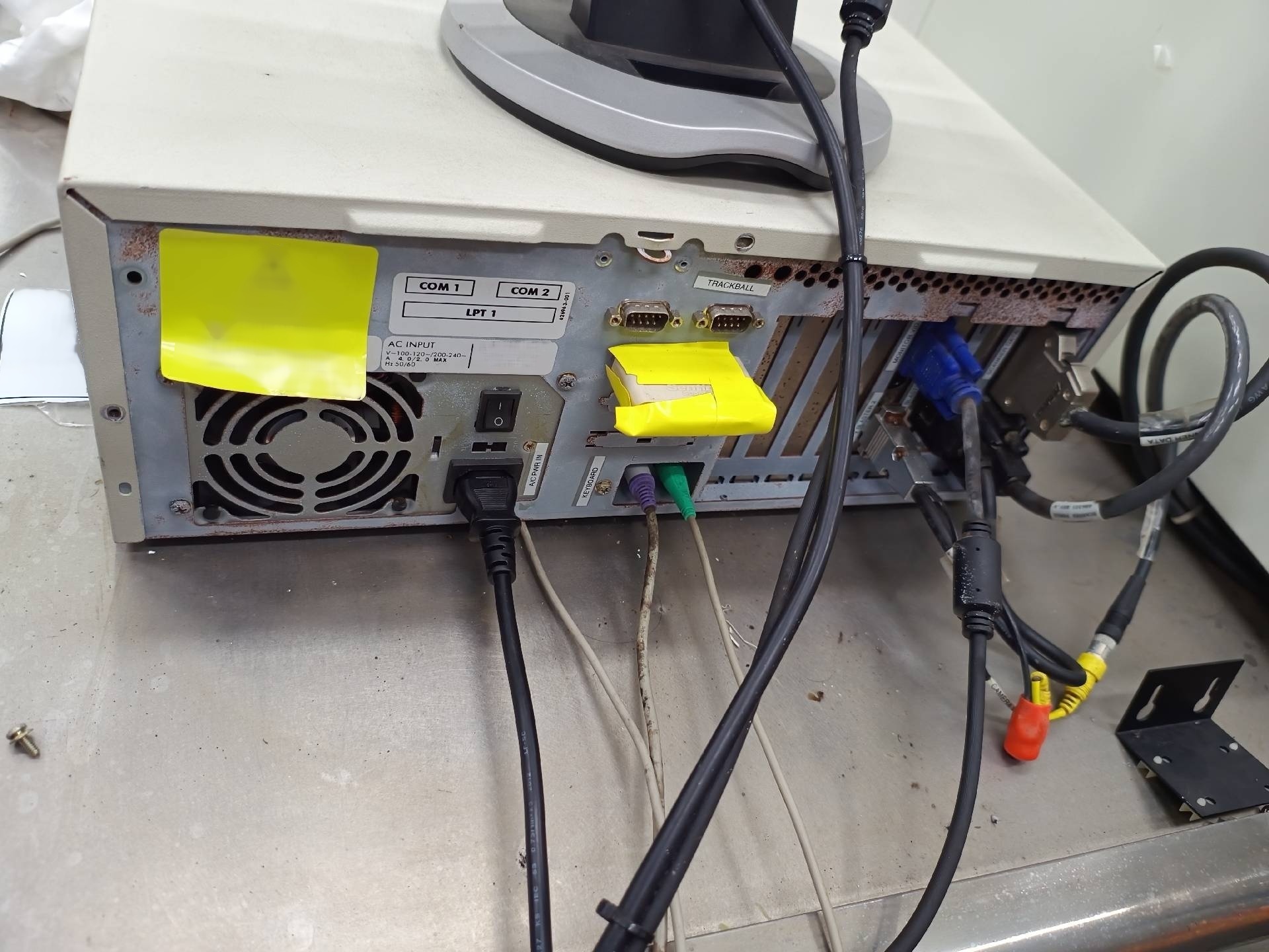
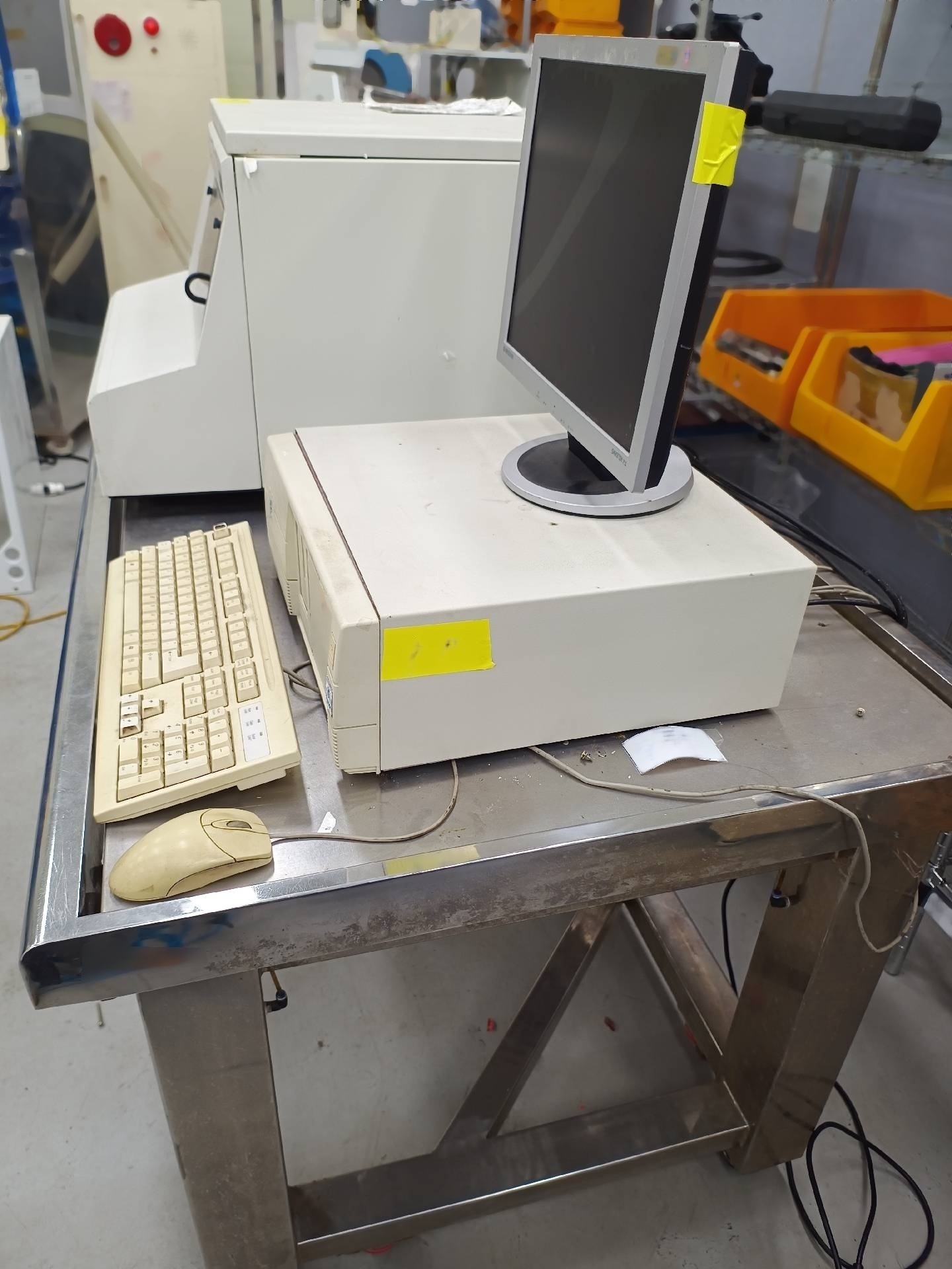
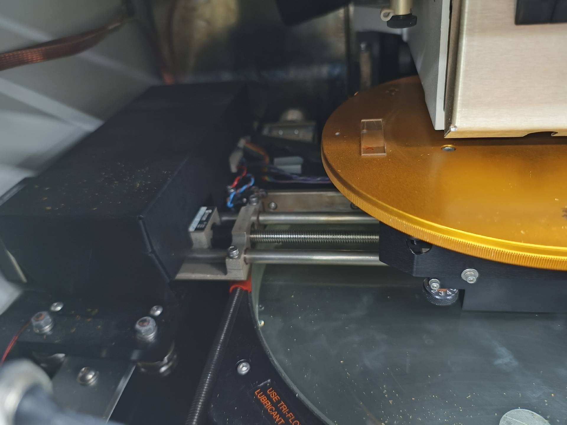
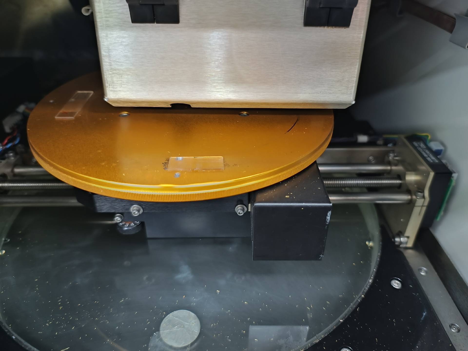
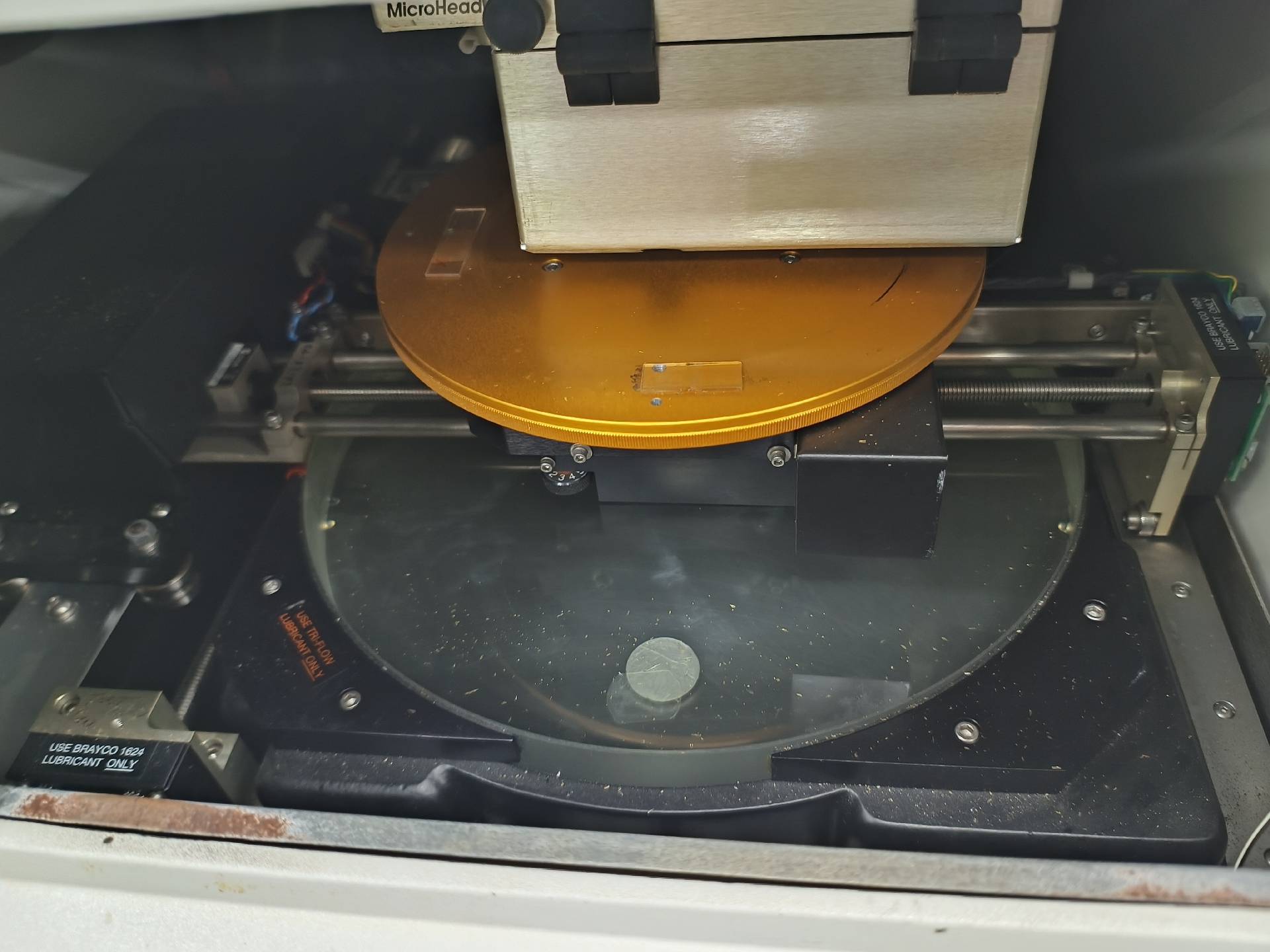
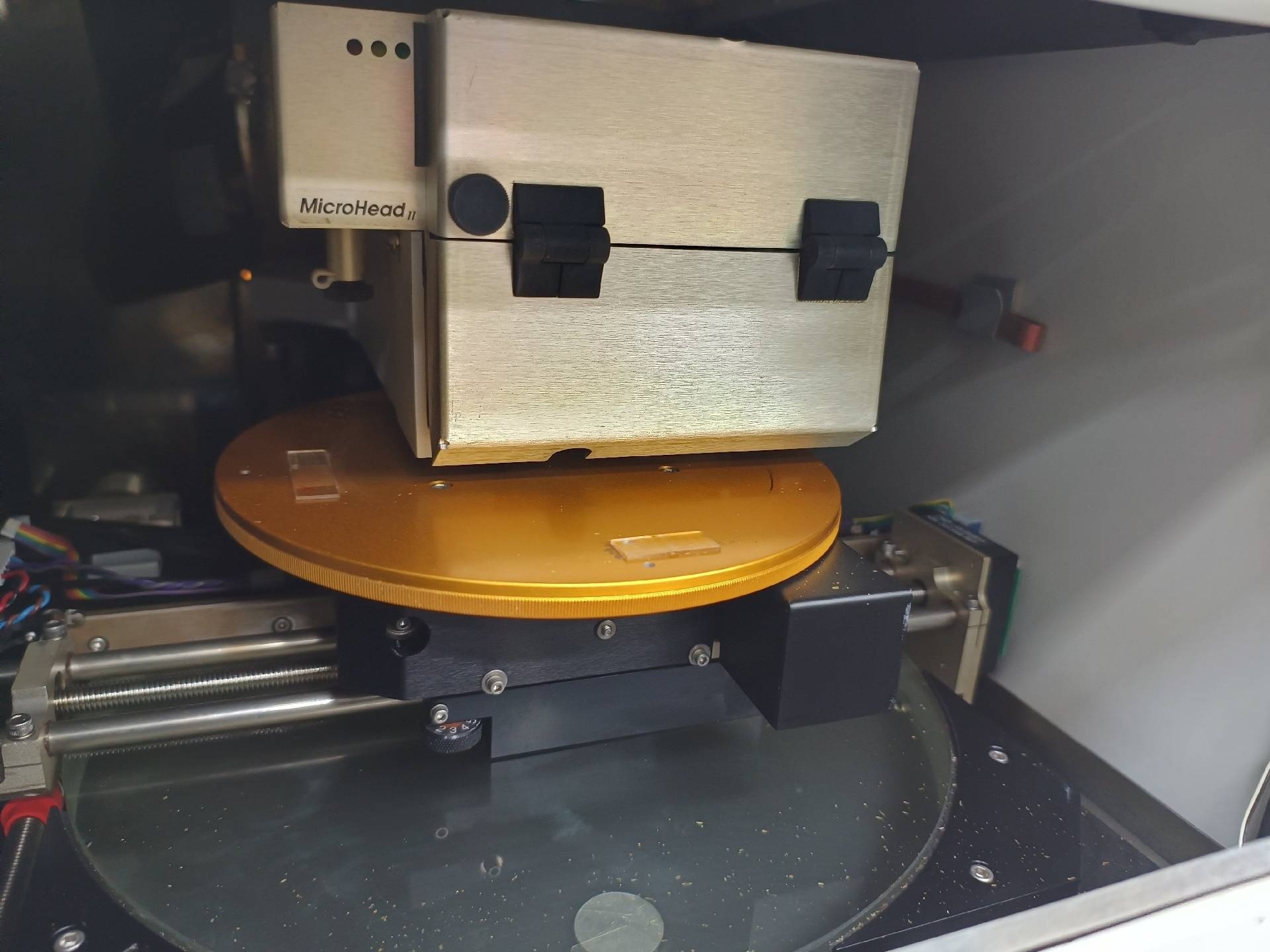
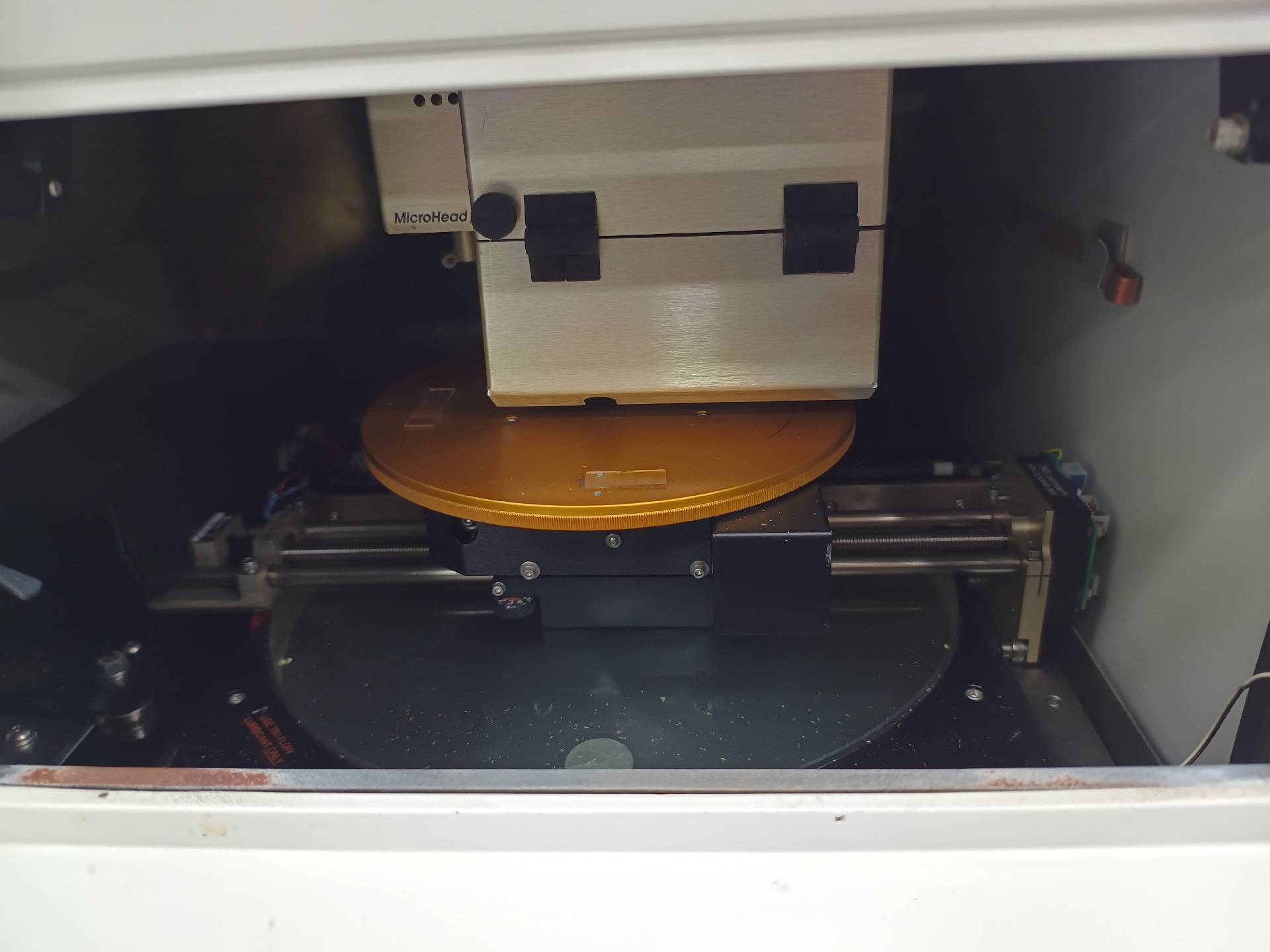
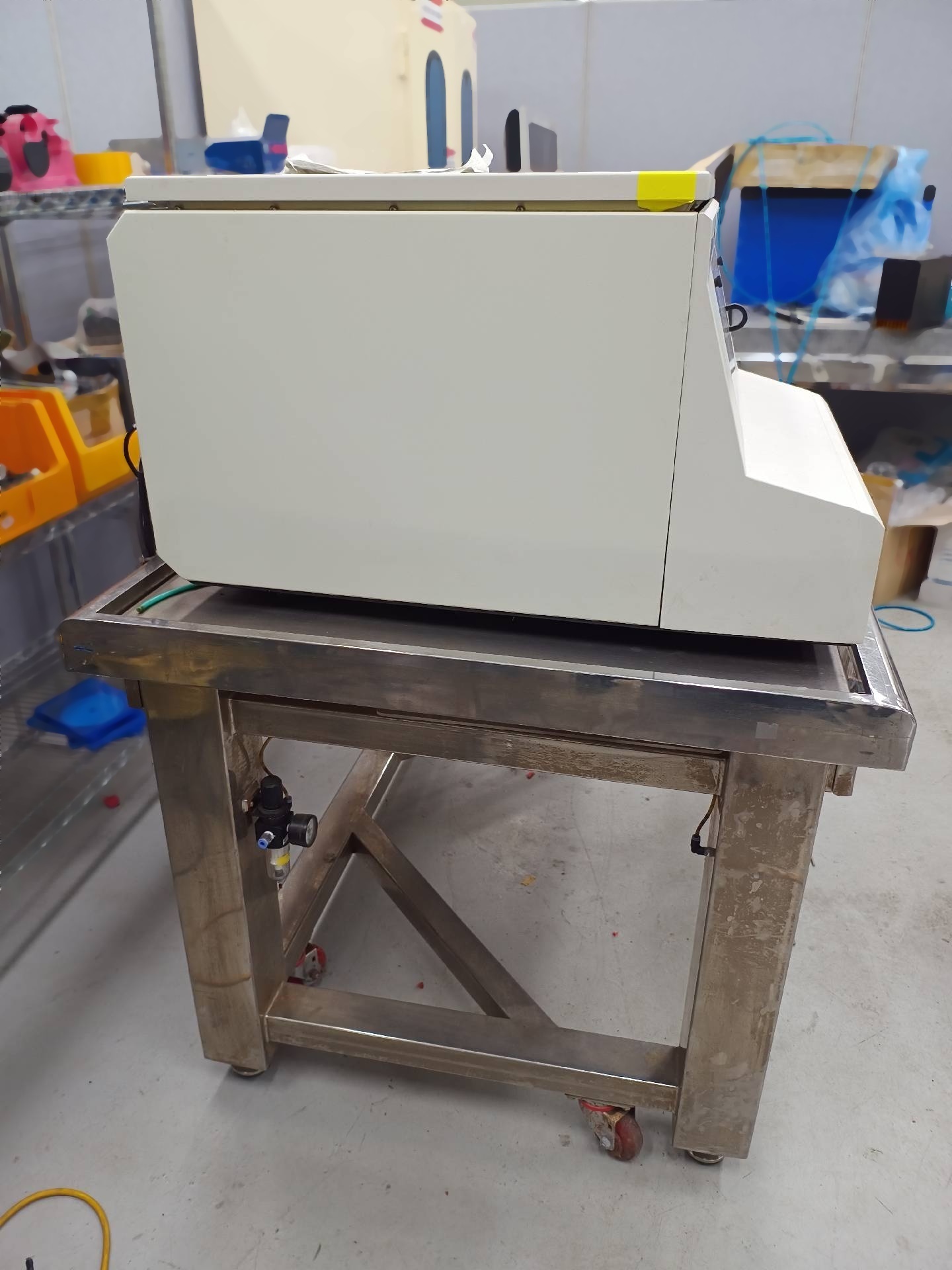
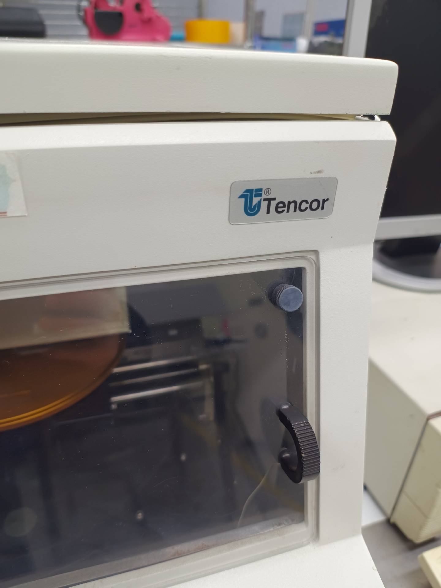
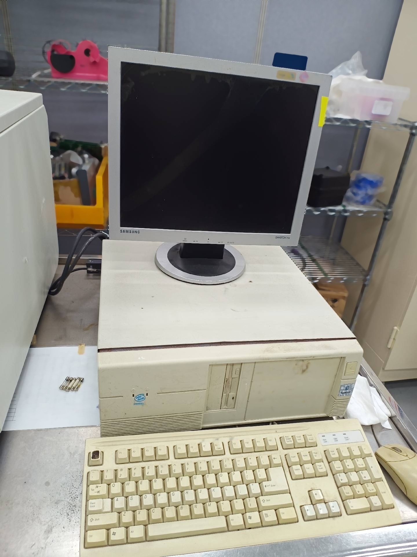
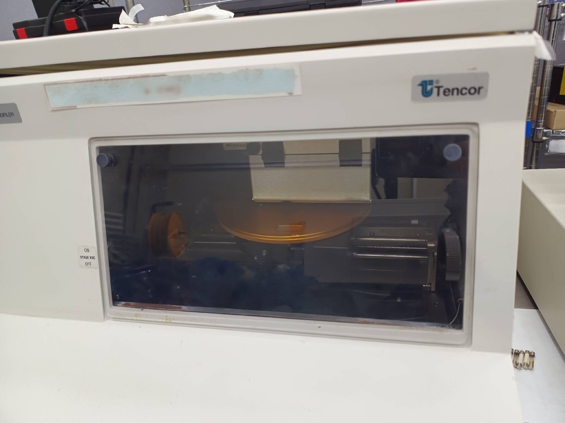
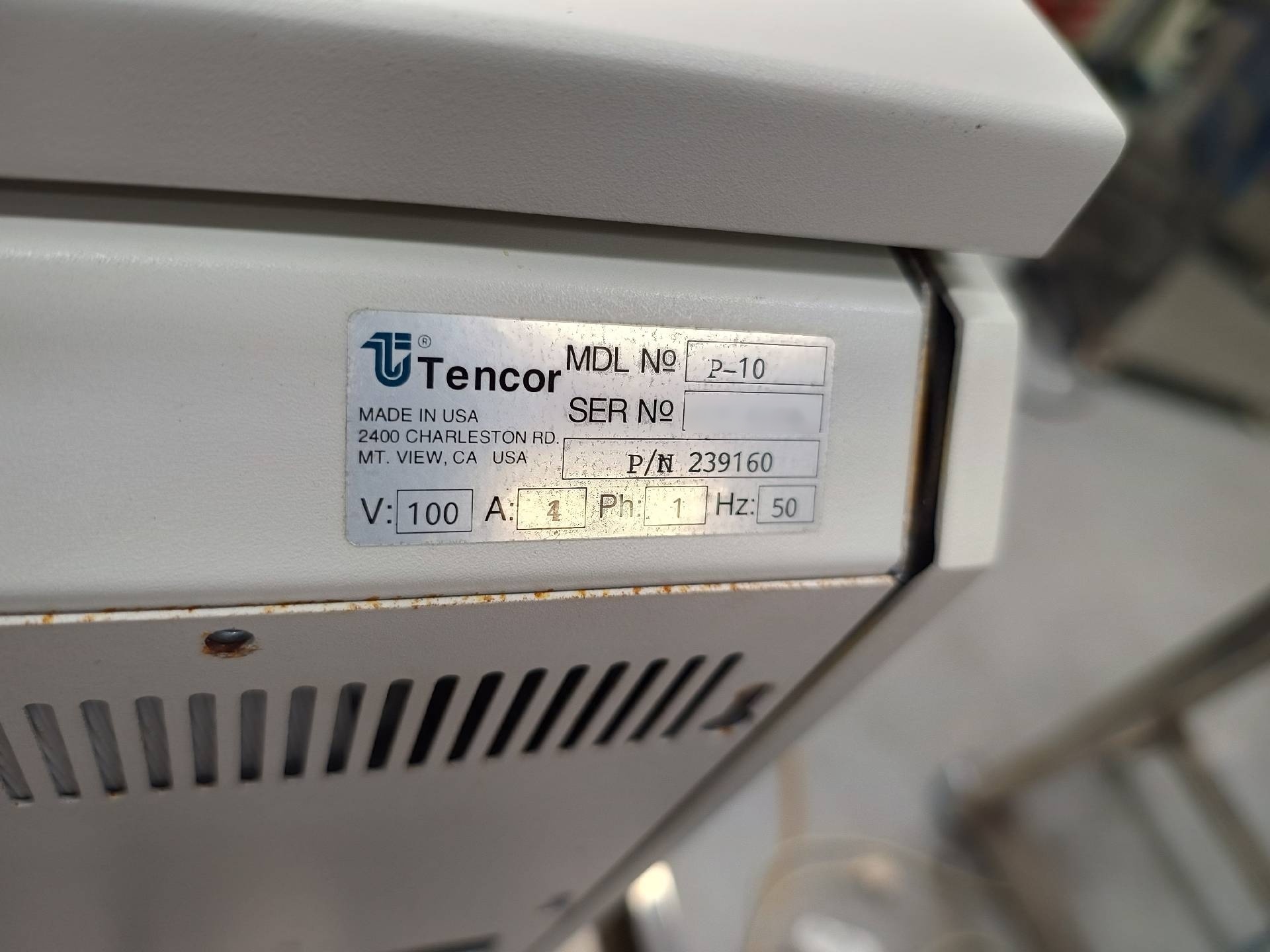
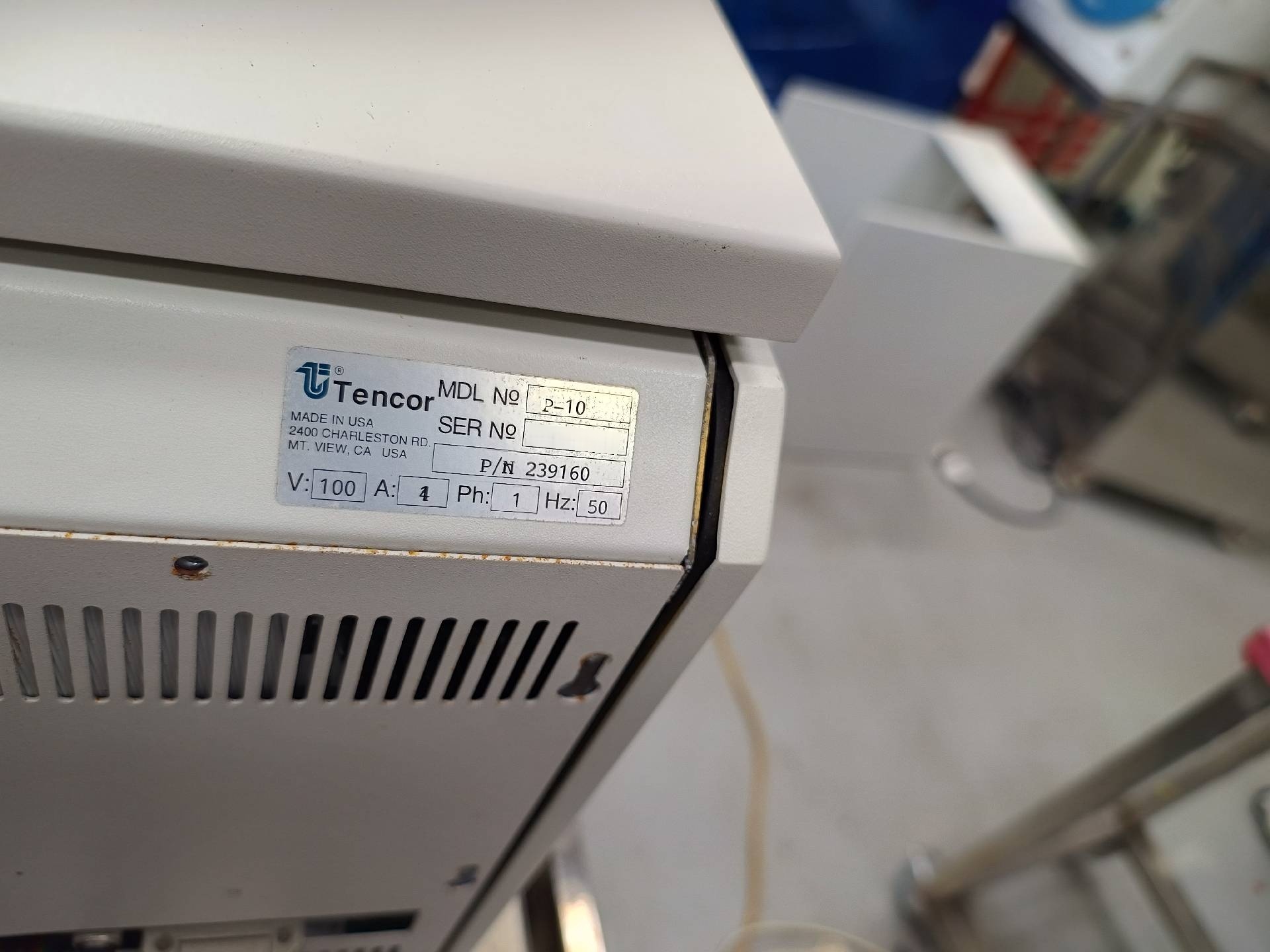
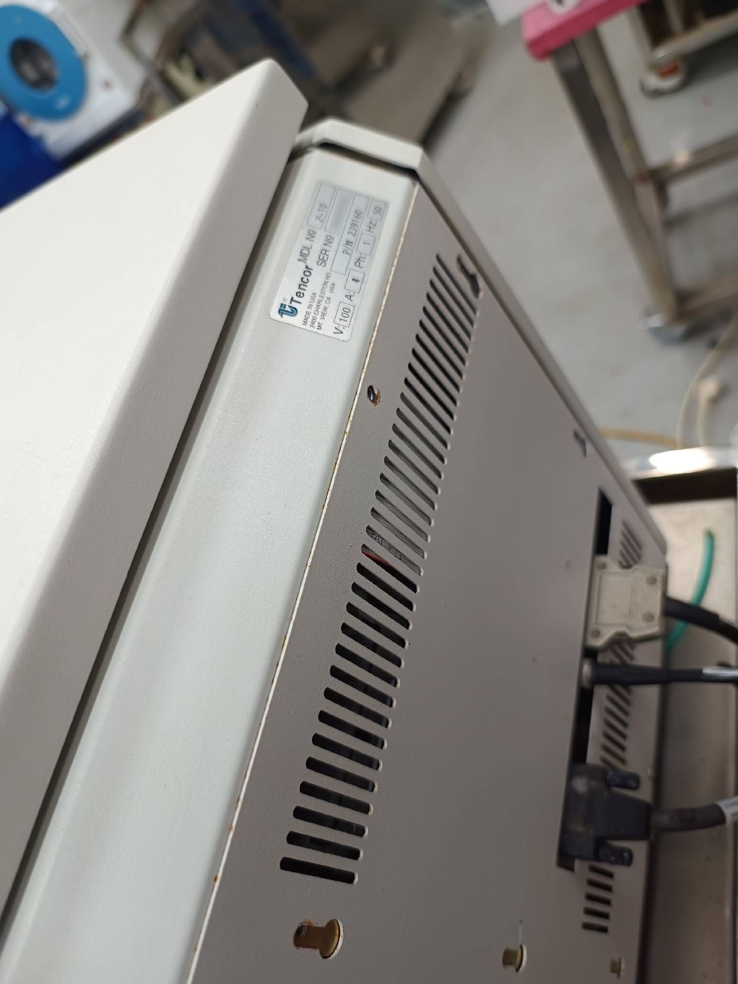
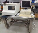
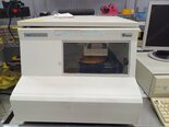
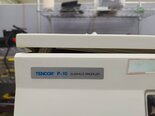
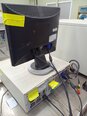
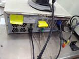
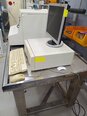
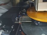
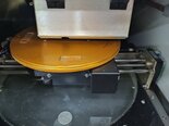
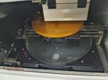
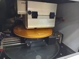
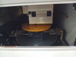
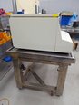
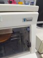
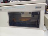
KLA / TENCOR P10 Wafer Testing and Metrology Equipment is a fully integrated, automated solution for wafer inspection and measurement, providing customers with the ability to detect and characterize defects, map device parameters and analyze wafer data. This system combines advanced imaging techniques, scanning electrochemical microscopy (SCEM) and resistivity testing, with a comprehensive suite of automated processes, enabling precise defect detection, analysis and reporting. At the heart of KLA P-10 is the Multi-Beam Velocity Scattering (MVSC) imaging technology. This unit uses a laser to scan the wafer surface at high speed, generating a high-resolution map of features, defects, and signature characteristics. The MVSC machine also detects material type and conducts resistivity testing to identify sample composition. TENCOR P 10 is also equipped with a micro-spectrometer, which provides the ability to quantitatively measure and characterize energy related data. The micro-spectrometer aids in the inspection and imaging of extremely small defects, as well as in characterizing materials with low reflectivity. In addition to imaging, KLA / TENCOR P 10 features a Scanning Electrochemical Microscopy (SCEM) tool. This asset uses a micron-scale-electrical current to probe the chemical structure of the wafer. By combining scanning electrochemical microscopy with MVSC imaging—TENCOR P10 is able to identify and characterize electrical etch marks, photoresist residues and other defects that are not typically detected with traditional imaging systems. KLA P10 also features a suite of automated processes including defect mapping, yield analysis, and reporting. These automated processes make it possible to inspect and measure wafers quickly and precisely, which is especially important for an industry where time is money. KLA / TENCOR P-10 Wafer Testing and Metrology Model is a revolutionary automated solution for wafer testing and metrology. Its combination of advanced technologies and automated processes enables the detection and characterization of even the smallest defects—leading to fewer costly defects and a higher yield.
There are no reviews yet