Used KLA / TENCOR P10 #293821173 for sale
URL successfully copied!
Tap to zoom
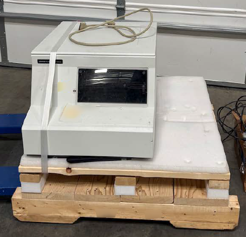

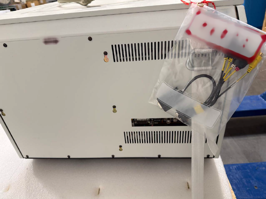
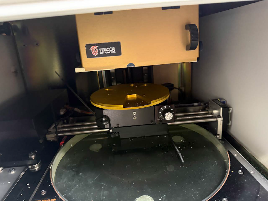
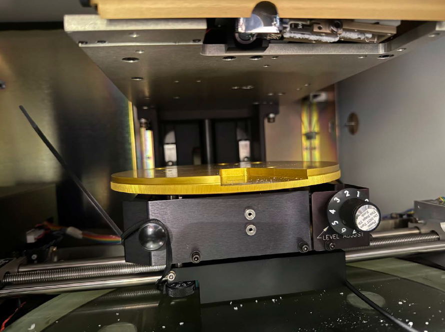
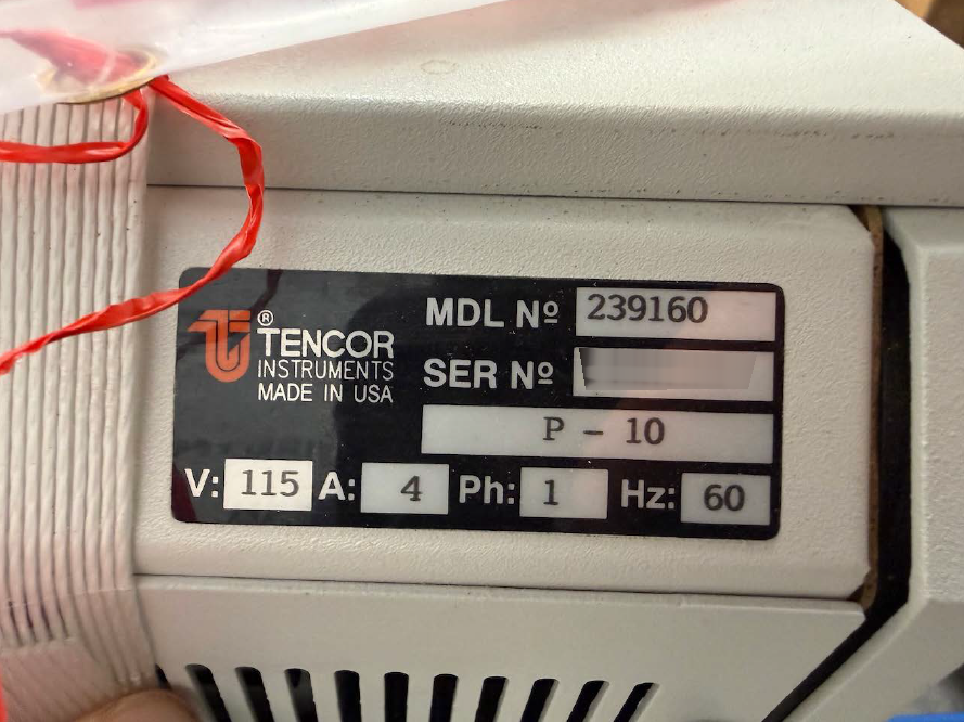
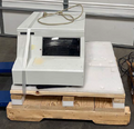
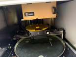
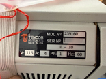
KLA / TENCOR P10 is a comprehensive wafer testing and metrology equipment designed to help silicon device manufacturers improve device yield, reduce manufacturing costs, and accelerate time-to-market. It offers both optical and electrical wafer inspection capabilities and is designed to be used in a wide range of production and technology development environments. KLA P-10 system provides significant performance advancements in terms of processing speed, accuracy, and overall unit size. It utilizes innovative, state-of-the-art optical metrology techniques and advanced optics. The machine contains a proprietary, high-speed embedded processor which can handle multiple tasks simultaneously, enabling faster image processing and data analysis. The tool can process up to 4,500 wafers per hour (wph). In addition to its high throughput performance, TENCOR P 10 asset provides a wide range of measurement capabilities. These include transistor level mapping capability, die-level defect inspection, micro-threading fault detection, 2D and 3D overlay measurements, double patterning and resist grading, film thickness analysis, and critical dimension measurement, among others. Furthermore, TENCOR P-10 model supports parallel optical, electrical and mechanical inspections, enabling a low-noise signal, faster measurements and wider range of detected defects. KLA / TENCOR P-10 also has a highly flexible equipment interface. Its open architecture supports easy connection to a variety of leading-edge wafer testing and metrology systems. Its extensive software library provides customers with complete control over parameters, reporting and process control. The system also offers pre-configured, user-friendly software packages specially designed for a range of standard IC analysis, allowing users to quickly create custom recipes with ease. In addition, KLA P10 includes advanced data visualization and extrapolation capabilities. Its graphic displays and interfaces provide a comprehensive view of wafer defect data. And its machine learning algorithms enable users to quickly spot issues and extract valuable insights from wafer data. Overall, P 10 wafer testing and metrology unit is an advanced technology that can provide significant benefits to producers of silicon devices. Its comprehensive and flexible design allows manufacturers to increase yield, reduce cost, and accelerate time-to-market.
There are no reviews yet