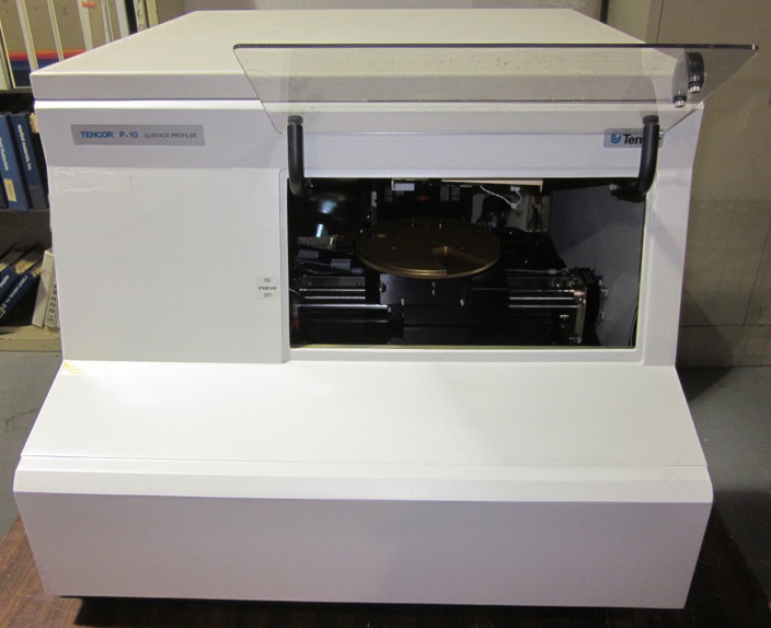
Used KLA / TENCOR P10 #9035604 for sale
It looks like this item has already been sold. Check similar products below or contact us and our experienced team will find it for you.
Tap to zoom


Sold
ID: 9035604
Wafer Size: 4"-5"
Vintage: 1996
Profiler, 4"-5"
Can add 6" & 8" wafer chucks - optional
Currently set up for wafers
MicroHead II low stylus force measurement head
Vertical ranges:
±3.2um at 0.004A resolution
±13 um at 0.016A resolution
131um at 0.08A resolution
Computer, monitor, keyboard & printer
Software: upgraded to KLA/TENCOR P12 software
3-dimensional and selected 2-dimensional data display
Scan length: 60 mm
Manual
1996 vintage.
KLA / TENCOR P10 is a high performance wafer testing and metrology equipment designed for advanced front-end semiconductor device testing. It features a highly reliable optical metrology system that is capable of extremely precise wafer and pixel level measurements on a wide range of semiconductor wafers up to 200 millimeters in size. The unit has an advanced vision machine that allows for the detection and analysis of features as small as a few nanometers, with the ability to measure wafer level features and resistance patterns. KLA P-10 is composed of several different components that work together to deliver accurate metrology measurements. Its optical metrology features are powered by a full-field optical engine, featuring a Continuous Optimized Wafer Trajectory (COWT) tool which makes full-field measurements possible. This COWT asset is designed to eliminate aberrations, which ensures accurate measurements on wafers with various shapes and levels of complexity. Additionally, TENCOR P 10 is coupled with an imaging module featuring a Wafer Extremity Level (WEL) model that can measure critical wafer levels with precision. KLA / TENCOR P 10 also features an industry-leading illumination equipment composed of both natural and artificial sources that are designed to deliver consistent measurements across the entire wafer surface. The system additionally contains a Low Angle Long Pitch (LALP) unit, which minimizes the image distortions due to curvature on modern wafers, ensuring accurate measurements at any angle. P-10 is designed to measure a variety of parameters including defect sizes, shape characteristics, film thickness, resistivity, and more. It utilizes Optic Security Version (OSV) technology to provide a secure data environment for confidential analysis of test results. The OSV technology integrates encryption, authentication, and secure networking capabilities that protect user data from potential outside interference. In terms of machine performance, KLA / TENCOR P-10 delivers high speed full-field metrology, with a read time of upto 40 wafers per hour, and accuracy of +/- 1nm, making it an efficient and reliable testing and metrology tool for wafers. This asset has a very streamlined user interface that allows for easy operation of the equipment, as well as the ability to store and view test results that are easily exportable for further analysis.
There are no reviews yet