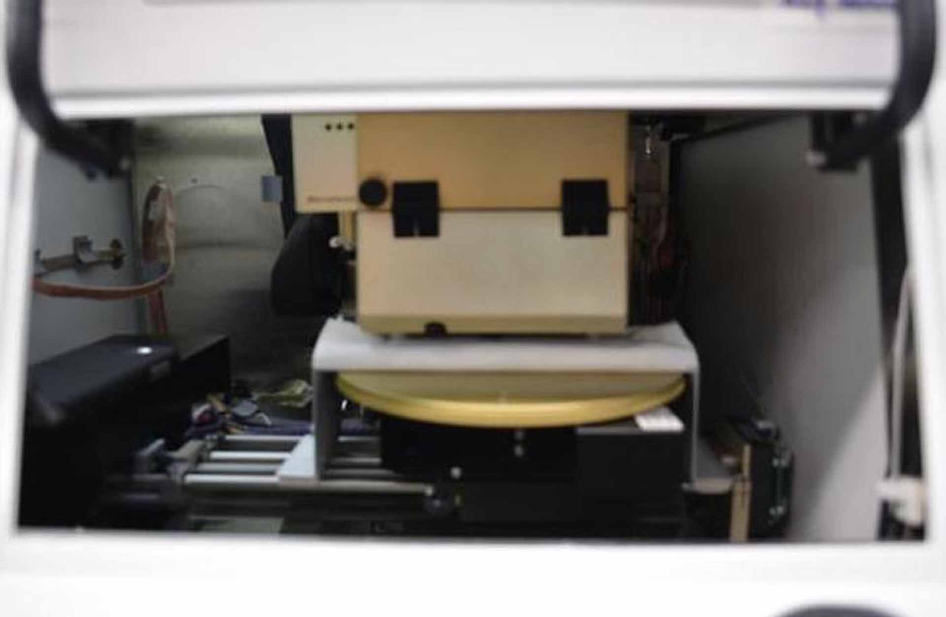
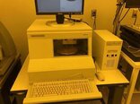
Used KLA / TENCOR P15 #293653975 for sale
URL successfully copied!
Tap to zoom


ID: 293653975
Wafer Size: 8"
Surface profiler, 8"
Upgraded from P10
Stylus
Wafer load profilometer
Scan length: 200 mm
Microhead II LF:
Maximum step height: ~131 µm
Stylus force: 0.5-50 mg
Step height: 6.5 µm, Resolution: <0.05 å
Step height: 26 µm, Resolution <2.0 å
Step height: 130 µm, Resolution <10.0 å
Top and side view optics
2D Stress analysis
Stress plate
Micro-roughness: 0.5 å (0.002 Minimum)
Vertical features ranging: 100 å (131 µm)
Vertical resolution: 0.05, 2, or 10 å
PC
LCD Monitor
USB Ports
Operating system: Windows XP.
KLA / TENCOR P15 Wafer Testing and Metrology Equipment is a high-precision tool designed to help identify and characterize defects, such as abnormality or contamination, on a semiconductor wafer. It is suitable for a variety of lithography and metrology processes, including sub-50nm device fabrication. The system is equipped with two large field of view optical heads, providing a full field of inspection with high spatial resolution. The unit includes advanced software algorithms to enable fast and accurate defect detection and classification. KLA P-15 also includes integrated metrology, allowing automatic measurement of critical dimensions, linewidths and overlay across the entire wafer surface. TENCOR P 15 is equipped with a Dual Image Capture Module (DICM), a modular high-resolution imaging machine capable of both bright-field and dark-field imaging. The DICM provides critical high-resolution optical imaging for precise defect analysis, enabling automated analysis of defect area, shape, and location on the wafer. KLA P 15 is also equipped with an Advanced Smart Cartridge (ASC), which provides intelligent scanning capability. The ASC enables thorough and systematic scanning of the entire wafer surface. Advanced wafer surface defect detection algorithms, including ISO 2645-compliant sparse and dense defect detection, are embedded in the tool. KLA / TENCOR P-15 includes a Results Analysis module, which provides powerful image comparison and defect classification tools. The Results Analysis module can automatically detect and classify defects, as well as measure critical dimensions, linewidths, and overlays. P-15 can be configured for automated review processes, enabling comprehensive and comprehensive analyses of defect data across multiple wafers. The asset also includes an extensive reporting capability to provide an audit trail for all defect-related activity. TENCOR P-15 Wafer Testing and Metrology Model provides a comprehensive solution for the detection, classification, and measurement of semiconductor wafers. The dual-image capture module, a modular high-resolution imaging equipment, and advanced software algorithms enable fast, accurate, and thorough analysis of defects and their related characteristics. KLA / TENCOR P 15 is suitable for fabrication of both standard and sub-50nm devices, and provides an audit trail for all defect-related activities.
There are no reviews yet

