Used KLA / TENCOR P15 #293798607 for sale
URL successfully copied!
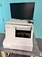
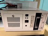
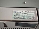
Tap to zoom


ID: 293798607
Surface profiler
Measuring range: 326-327 µm
Vertical resolution: 0.5 A
Step height measurement range: 100 microns
Maximum sample size: 6"-8"
Maximum sample thickness: 20 mm
Probe: 2 µm
Load range: 1 mg
Stylus tip: 2 µm / 60°
Stylus force range: 1 mg to 50 mg
Scan mode: 2D Line scan / 3D Surface mapping
X-Y Scanning resolution: 0.1-1 µm.
KLA / TENCOR P15 wafer testing and metrology equipment is a state-of-the-art tool designed to provide a comprehensive suite of metrology for semiconductor technology. KLA P-15 features patented dual detection laser technology and the OptiSpec manual cup™ which enables the system to measure both high-resolution physical defects and advanced parametric measurements ranging from linewidths, critical dimensions, and overlay simultaneously. The high-speed linear generation of advanced laser beams combined with complimentary laser optics and digital signal processing offers single-beam accuracy. The patented dual detection laser technology also enables the unit to function with high performance at a low operating cost. The machine is equipped with seven scanning range options of up to 20mm along the x-axis and 8 mm along the y-axis allowing for multiple measurements across the sample of interest. Additionally, TENCOR P 15 features a mechanical scanner with monochrome offset motion control, enabling precise positioning and gentle delivery of the sample. P15 is also optimized for fast, efficient operation. The tool can be easily set up and programmed, making it suitable for use in laboratory and production environments. The onboard scan engine is optimized for maximum throughput and includes advanced error-correction algorithms and low-noise design to ensure precise, repeatable results. Furthermore, KLA / TENCOR P 15 is equipped with an optically variable chip (OVC) and die mounting table (DMT) which help to ensure that the measurement data reflects the measurements taken on the sample as accurately as possible. Additionally, TENCOR P-15 visual inspection optics allow for high-resolution imaging and metrology of features as small as 0.1 microns. The asset's integrated processing unit is powered by the Autodrive™ which helps to streamline the sample preparation and analysis process. Overall, KLA / TENCOR P-15 wafer testing and metrology model is an advanced metrology tool designed for semiconductor technology and offers excellent precision, speed, and accuracy. The equipment allows for multiple measurements in a single scan and is equipped with high-resolution imaging and metrology optics, advanced laser technology, and digital signal processing. Furthermore, the system is configured with an optically variable chip and die mounting table to ensure the highest level of accuracy and repeatability.
There are no reviews yet