Used KLA / TENCOR P15 #293809526 for sale
URL successfully copied!
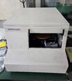
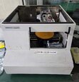
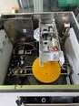
Tap to zoom
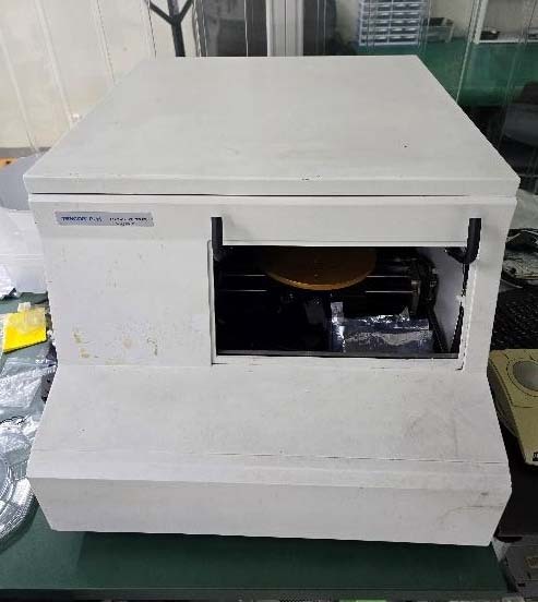

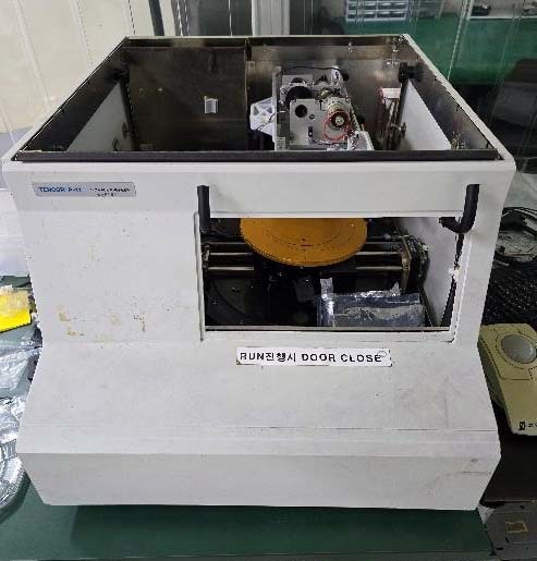
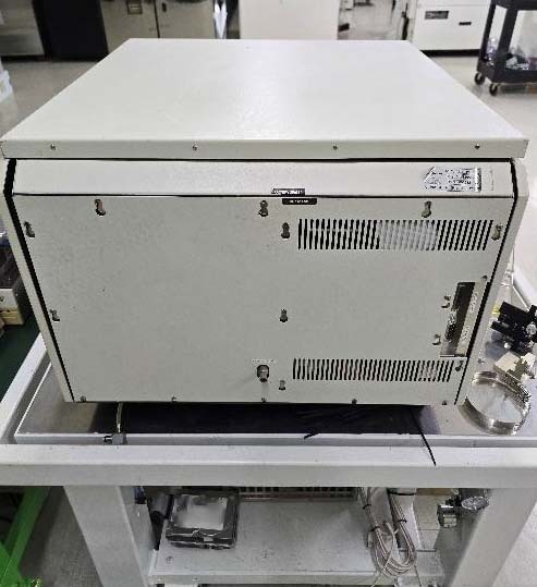
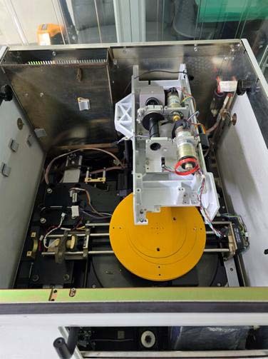
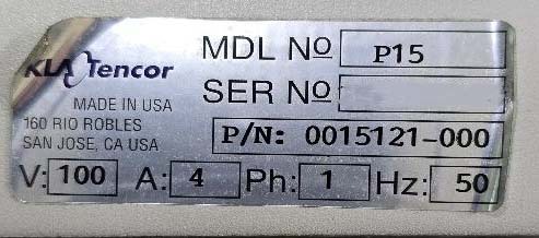
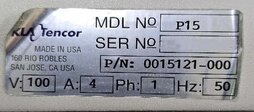
KLA / TENCOR P15 is an advanced wafer testing and metrology equipment designed for the semiconductor industry. The system is outfitted with high-resolution cameras and image processing software, enabling it to accurately detect and measure defects on wafers with a high degree of accuracy. The unit is also equipped with multi-sensor and multi-measurement technology, making it capable of multiple measurement types, including thickness, flatness, crack detection, and three-dimensional imaging. The machine is built around an inline inspection architecture which features an integrated feeder, prober, mapping stage, and wafer-level coaters. This architecture eliminates any transfer step, allowing high-throughput wafer testing. Furthermore, the tool's advanced imaging algorithms identify and classify defects based on parameters such as shape, contrast, and size. This architecture also simplifies dual-tool operations, enabling KLA P-15 to inspect and measure on a single wafer without complex asset reconfigurations. The model is also equipped with KLA C Series inspection and metrology software, featuring advanced metrology capabilities and cycle time optimization software. This software enables users to perform a wide range of inspections including edge exclusion, line width determination, CD flatness, CD profile, etch depth, thin-film thickness, and CD tilt. Additionally, the software also provides robust algorithms for tool-to-tool and pattern-to-pattern correlation, plus statistical process control and yield analysis. TENCOR P 15 is capable of measuring both bulk and device structures on all semiconductor materials, including silicon, germanium, and gallium-arsenide. Furthermore, its automated calibration and prod-level workflows greatly reduce setup times, enabling users to get the equipment up and running quickly. The system is also equipped with high-performance air bearing stages, providing smooth wafer motion and precise wafer positioning. Overall, P15 is an advanced wafer testing and metrology unit designed for use in the semiconductor industry. The machine's high-resolution cameras and image processing software are capable of accurately detecting and measuring defects on a variety of different wafers. Additionally, its built-in multi-sensor and multi-measurement technology makes it capable of performing a variety of different measurements on a single wafer. Furthermore, the tool's TENCOR C Series inspection and metrology software offers robust metrology capabilities and cycle time optimization software, enabling users to conduct both basic and sophisticated inspections quickly and easily.
There are no reviews yet