Used KLA / TENCOR P16+ #293815639 for sale
URL successfully copied!
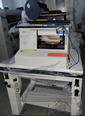
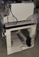
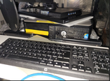
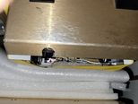

Tap to zoom
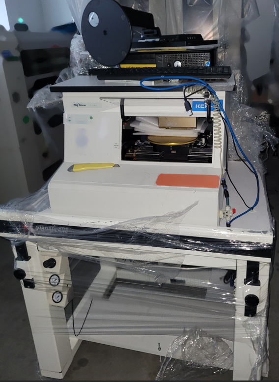

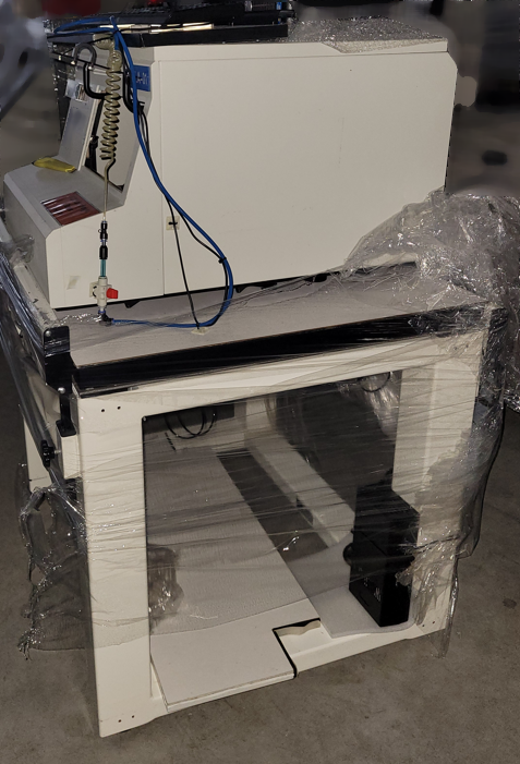
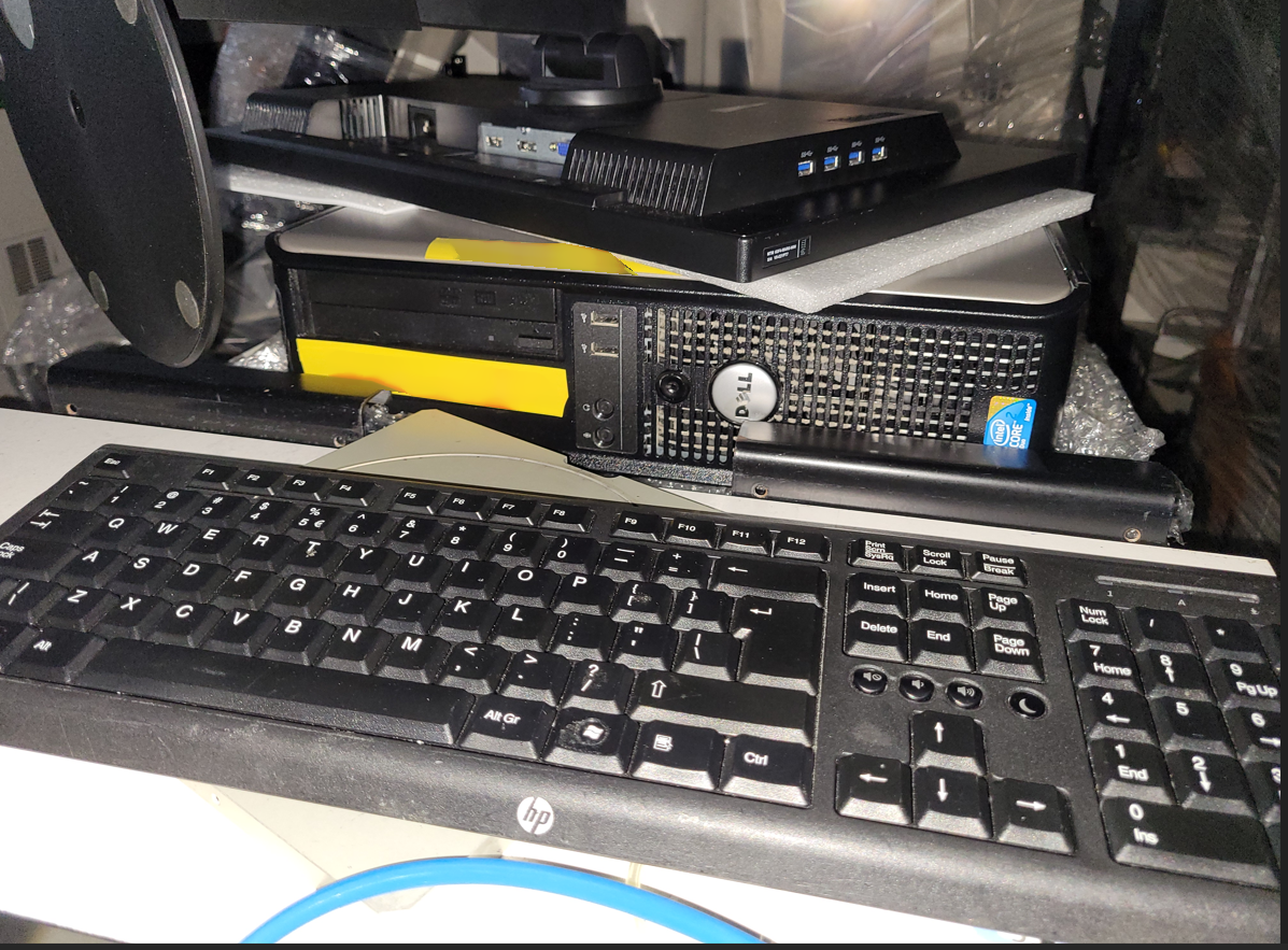
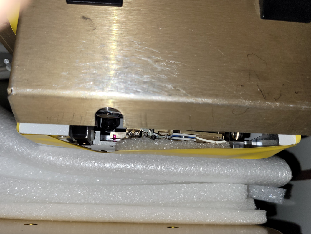
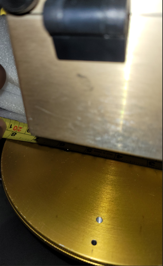
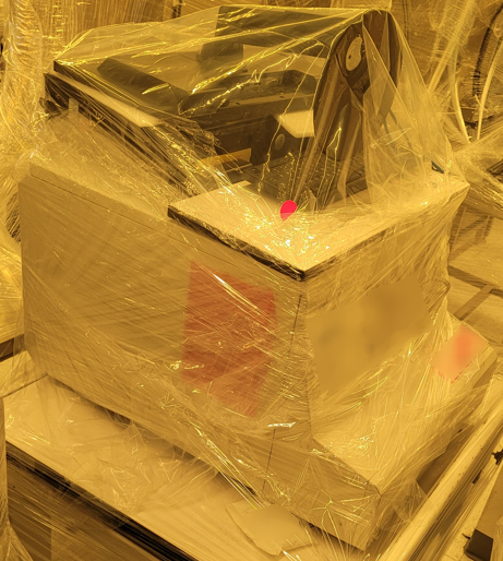
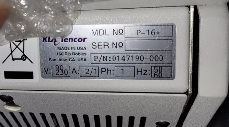
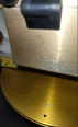
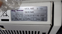
KLA / TENCOR P16+ equipment is an automated wafer testing and metrology system designed to provide comprehensive metrology solutions for the semiconductor industry. It uses advanced algorithms and proprietary sensing technology to measure and analyze wafers quickly and accurately. KLA P 16+ can be used to measure the thickness, failure analysis, and topography of wafers and other substrates with a range of thicknesses between 0.8 and 32 microns. The unit can also be configured for various levels of optical testing, including process monitoring and detailed defect analysis. TENCOR P-16+ is equipped with a sophisticated optical inspection machine featuring a multi-wavelength laser illuminator, which can be used for a variety of tests, such as reflection and refractive index measurements. The unique multi-wavelength optics allows the tool to perform beyond NIST traceable qualification tests. The asset also uses a modular probe head with interchangeable lenses and stage plates for high precision sampling and measurement. KLA P-16+ is also capable of capturing a wide range of electrical test signals in either an analog or digital format. This interlaced feature enables test characterization, process monitoring tests, and fault analysis. Additionally, the model includes sophisticated embedded software and powerful analytical software tools for easy data capture and analysis. KLA / TENCOR P-16+ equipment is available in a variety of configurations depending on user needs and budget. KLA / TENCOR P 16+ system includes an automated wafer mapping unit to accurately measure across each wafer surface for up to 3,000,000 points. It is also equipped with an innovative cross-section imaging machine that enables the user to accurately analyze three-dimensional structures of scanned objects. Overall, KLA P16+ Wafer Testing and Metrology Tool delivers superior performance and accuracy for all types of production and research applications. Its advanced optical inspection asset, automated wafer mapping model, and powerful analytical software make it an ideal choice for semiconductor producers and researchers.
There are no reviews yet