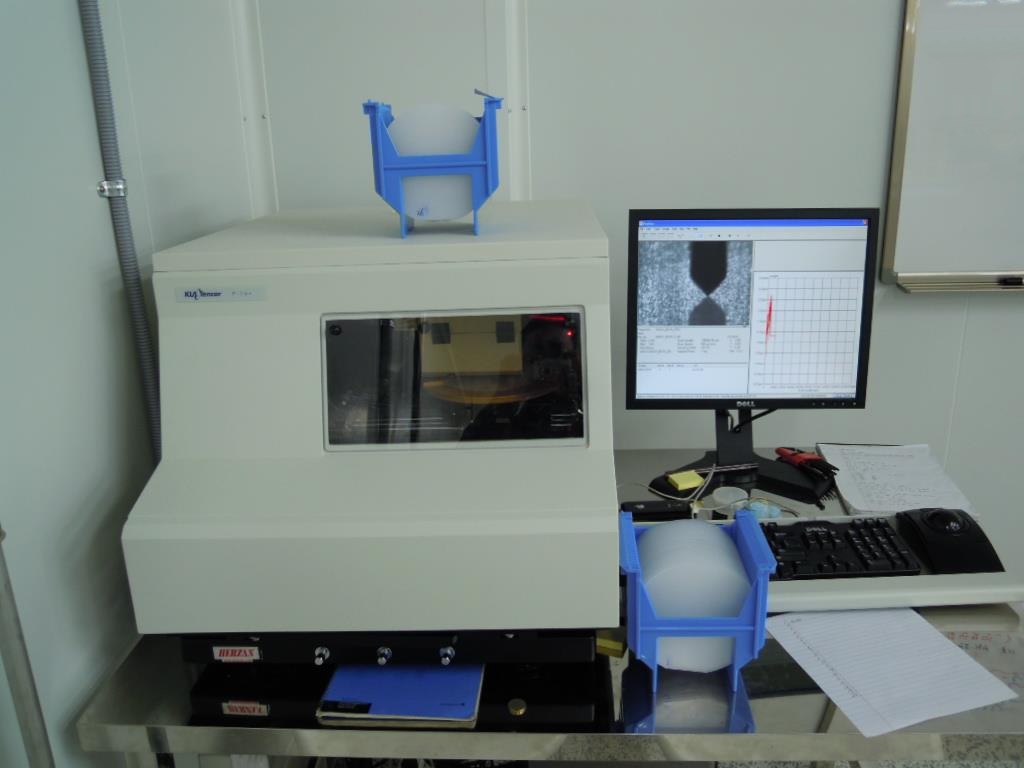
Used KLA / TENCOR P16+ #9148051 for sale
URL successfully copied!
Tap to zoom


ID: 9148051
Surface profiler
Lapping
Measurement method: long-scan contact linear scans
Vertical resolution: 0.2 Å @ 327 μm
Step height repeatability: 6 Å, 100nm step
Profile data points: 4,000,000
Scan length: 80 or 200 mm
Maximum Z range: 1 mm
Stage translation: 240 mm x 240 mm
Sample positioning: motorized <1 μm
Sample stage diameter: 200 mm
Stylus force: 0.05 mg- 50mg
Field of view: 1.0mm - 4.0mm
Scan speed: 2 μm/sec to 25 mm/sec
Relative humidity: 30~40% (non-condensing) recommended
Temperature: 16℃~25℃, rate of change ≤2° C/h
Vacuum: 500 mm Hg @ 27 liters/min
Electrical: 220V, 60Hz, 430VA.
KLA / TENCOR P16+ is a wafer testing and metrology equipment designed to provide high performance inline metrology and defect inspection within the semiconductor industry. The system offers advanced tool capabilities combined with an intuitive user interface to allow for fast, consistent, and reliable test results. KLA P 16+ is a next generation unit that provides die-level multichannel semiconductor wafer inspection, both in terms of detection sensitivity and rapid data throughput. TENCOR P-16+ machine provides industry-leading wafer defect detection accuracy and performance. The tool is equipped with advanced quad-channel detector technologies that allow it to accurately detect defects in various mask layers and defect sizes. It features nanometer lateral resolution and provides superior pattern recognition algorithms that enable high-accuracy defect detection and classification. The asset provides rapid automatic recognition of spatial array types, such as DPTs, corners, scopes, and surface mount components. In addition to defect detection, TENCOR P16+ model also offers inline metrology capabilities. It offers a variety of sophisticated metrology techniques, such as CD-SEM, scatterometry, and ellipsometry, to measure both vertical and lateral dimensions and distortions on the wafer surface. It also provides through-silicon-via (TSV) CD-SEM measurements, defect tracking, and placement of test patterns on the wafer. The equipment is equipped with an advanced optical profiler module that offers advanced light scattering and image-processing techniques for fast and accurate metrology measurements. KLA P-16+ system is easy to operate, reliable, and compatible with various automation schemes. Its operator-friendly interface allows for easy operation, with the ability to customize test plans and settings for specific applications. The unit also offers sophisticated data management capabilities, with real-time data analysis and reporting capabilities. Its user-friendly features help streamline the operation and inspection process, resulting in improved productivity and quality assurance. Finally, TENCOR P 16+ is built for reliability, durability, and cost-efficiency. It offers robust and reliable designs that meet the highest international standards, making it suitable for all production environments. The machine is built to reduce downtime, costly repairs, and maintenance costs, leading to maximum productivity and profitability. In conclusion, P16+ is a powerful wafer testing and metrology tool that offers advanced tool capabilities and reliable performance. It provides high accuracy defect detection and inline metrology capabilities, making it suitable for a variety of applications within the semiconductor industry. The asset is designed for ease of use, reliability, and cost-effectiveness, resulting in improved quality and productivity.
There are no reviews yet