Used KLA / TENCOR P17 #293814734 for sale
URL successfully copied!
Tap to zoom
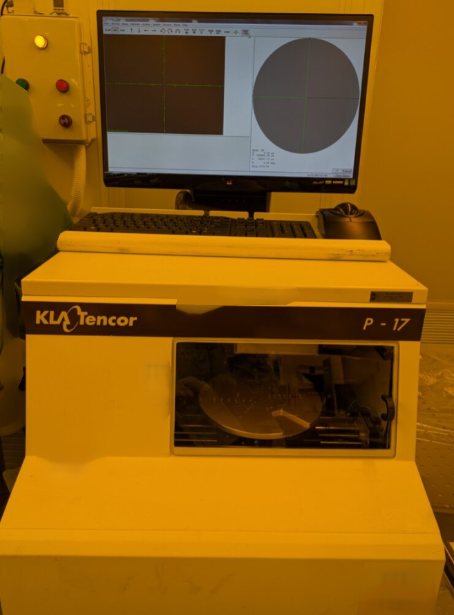

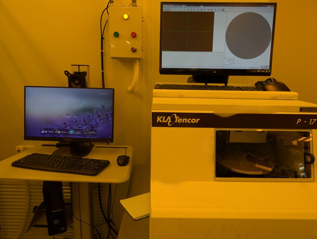
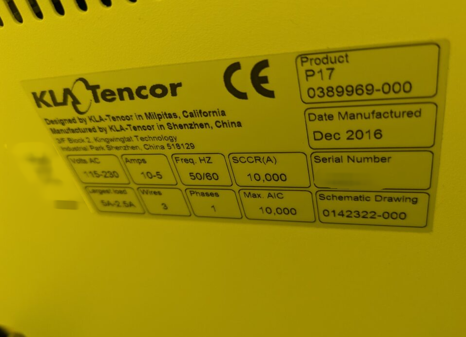
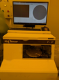
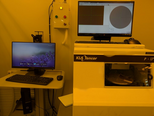
KLA / TENCOR P17 is a high performance wafer testing and metrology equipment, built on a robust and flexible platform to accommodate a wide range of semiconductor devices. This system employs advanced optics and metrology algorithms to provide accurate and precise results, enabling engineers to measure, process, and analyze data quickly and accurately. KLA P-17 unit is equipped with state-of-the-art components, including a large 6-color CCD camera with high resolution, a high-quality liquid crystal display (LCD) for visual viewing, a mobile-sized spectrometer, and an optical comparator. This setup allows for comprehensive wafer testing and metrology capabilities, including defect classification, particle identification, surface inspection, line width measurement, and thickness measurements. TENCOR P 17's high resolution camera enables it to capture microscopic images of wafers with great detail, allowing engineers to analyze individual pixels for surface features and defects. Through the use of algorithms, engineers can measure features such as line widths and surface topography with precision. The presence of various defect types can also be determined through the automated detection of particles, which are separated and identified according to size, shape, and position. In addition to this core set of capabilities, KLA / TENCOR P-17 also offers a variety of additional features, such as data analysis and reporting capabilities, statistical process control, and automated defect inspection. This multi-functional machine is capable of capturing, processing, and analyzing data from a variety of substrates, including silicon wafers, MEMs devices, and other integrated circuits. Overall, KLA P17 tool is a powerful and reliable tool that provides high accuracy and reliability at an affordable price. It can be utilized to measure, process, and analyze a wide variety of substrates and help engineers identify and reduce defects in order to improve the quality and performance of their products. With its sophisticated features and capabilities, P 17 wafer testing and metrology asset provides a dependable solution to a key challenge in the semiconductor industry.
There are no reviews yet