Used KLA / TENCOR P2 #293800218 for sale
URL successfully copied!
Tap to zoom
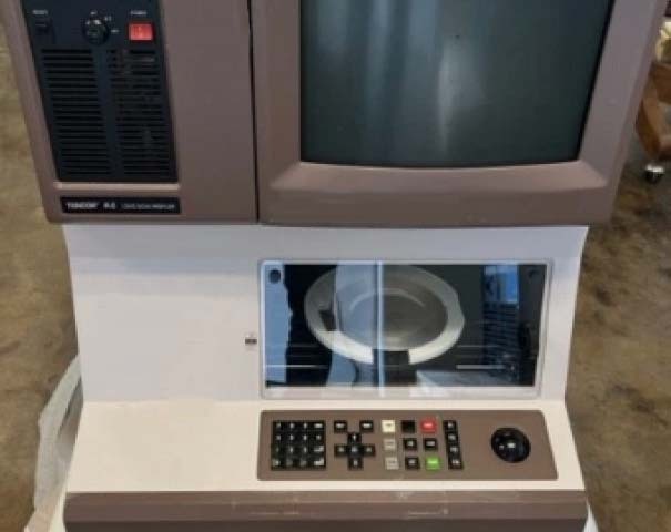

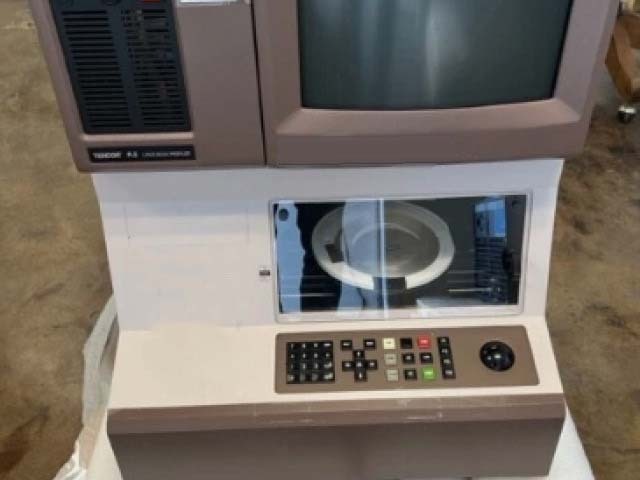
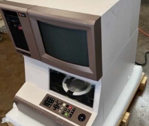
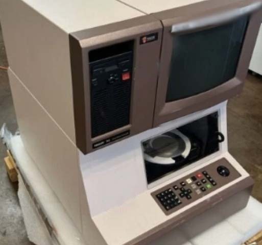
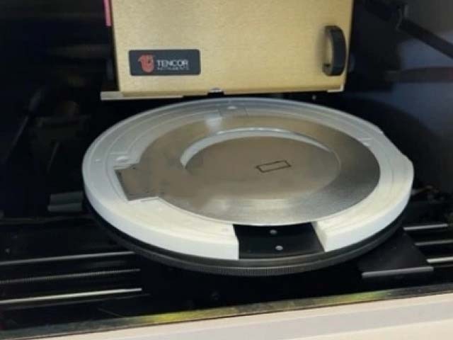
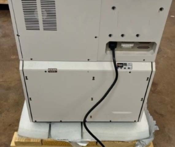
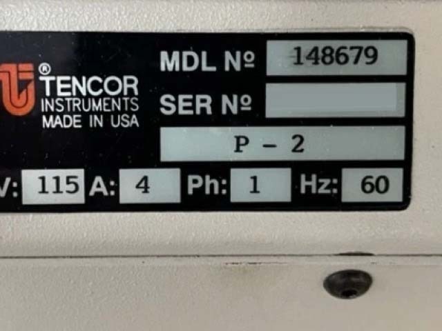
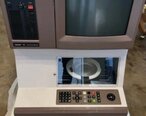
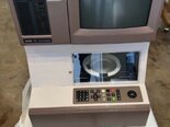
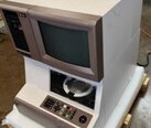
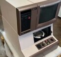
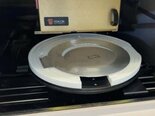
KLA / TENCOR P2 is a wafer testing and metrology equipment optimized for the most demanding wafer fabrication applications. It provides a comprehensive array of inspection and measurement capabilities, with high resolution images, fast scanning speed and small size. KLA P-2 enables non-contact metrology measurements to quantify non-uniformly thinned wafers and thin films, while also offering laser interferometry and micron-level coordinate-measuring-machine (CMM) capabilities. The system uses scanning electron microscopy (SEM) imaging to better access topography and to detect defects. TENCOR P 2 is designed with advanced hardware and software technology to optimize throughput and performance. The unit's optics are adjustable to accommodate a range of wafer sizes and dimensions. The Scanning Electron Beam (SEB) is designed to obtain the highest resolution images and measurements. The spectrometer—the automated machine for acquiring spectra and making 3D measurements—employs multiple modal sensing for fast and accurate characterization. TENCOR P2's high-end control software includes features such as cluster tool automation, auto sample recognition, and integrated factory-wide tools. The advanced software also provides auto alignment and distortion correction, which minimize the effects of sample eccentricity. This sophisticated software automates the process of acquiring measurements from multiple sites on the same sample. TENCOR P-2 is capable of simultaneously measuring thin layers, wafers, and thin films using the software's multi-wavelength amplitude modulation (MAM) technique. This technique can reduce measurement uncertainties by providing accurate, repeatable results. To facilitate easy viewing and data transfer, the tool also integrates an HDTV camera and support for DataBridge software. DataBridge allows in-line data transfer and analysis, thus enhancing the accuracy and speed of analysis. This enables faster decision-making and project completion. P-2 is an advanced wafer testing and metrology solution optimized for fast, accurate, and repeatable performance. With its cutting-edge hardware, software, and sensors, it offers the best combination of speed and accuracy for inspection and measurements across a wide range of wafer fabrication applications.
There are no reviews yet