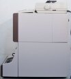
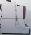
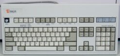
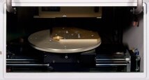
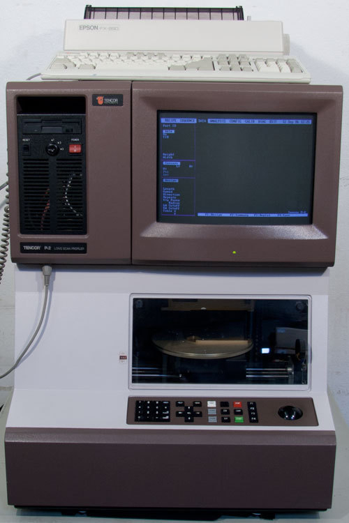
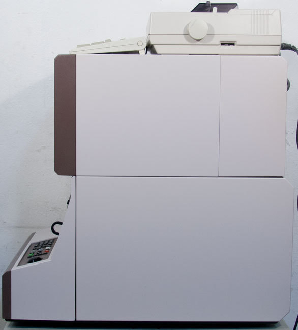
Used KLA / TENCOR P2 #9007474 for sale
URL successfully copied!
Tap to zoom


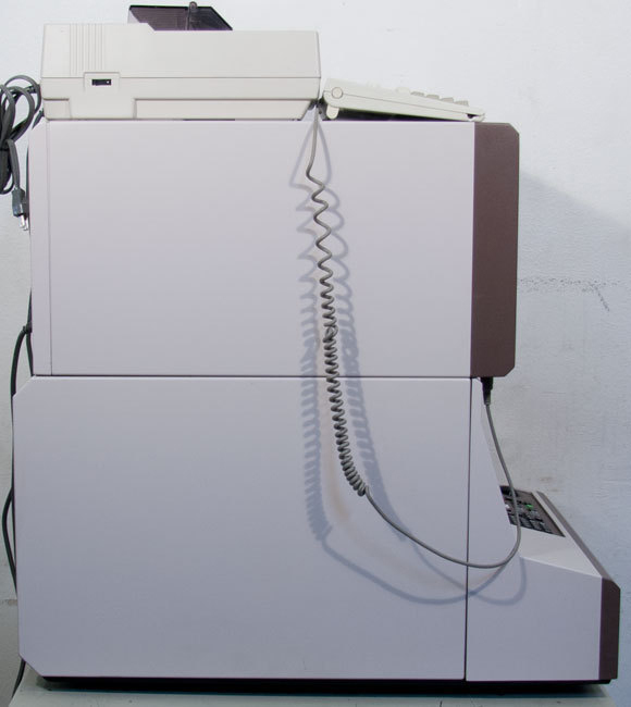

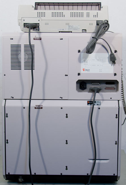


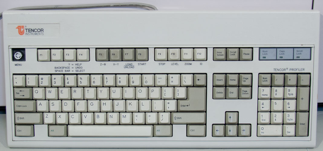

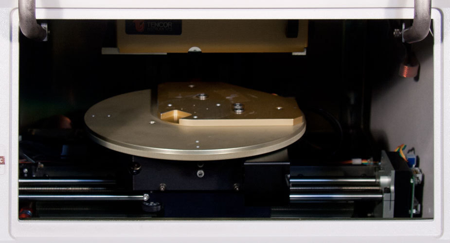

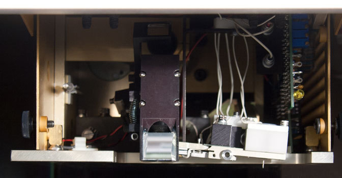

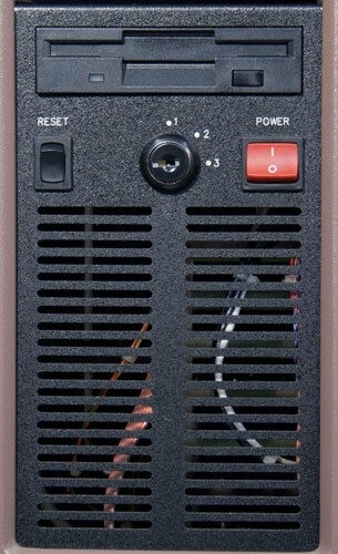

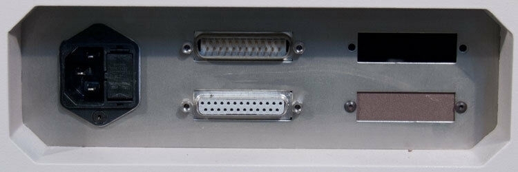

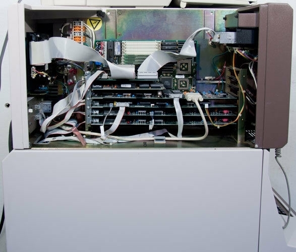

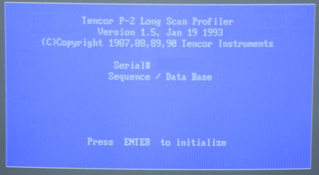

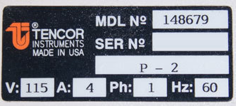

ID: 9007474
Automated long scan profilometer
Optic: 150-600X HI
Stylus force:
0: 226
10: 339
40: 557
100: 840
300µ Range: 0.9975
Scan length: 0.0000000
Backlash: 0
Drop timer: 27
Linearity:
A: 975
B: -350
Options:
Sequence / Data base manager option
Motorized level and rotation option
Measure micro-roughness with:
1 Å resolution over short distances scan: 210 mm (8.2")
PC / AT Computing power automatic measurement capability
Data storage
Data analysis
Includes:
Magnetic disks
Semiconductor wafers
Precision-machined and polished surfaces
Ceramics for micro-electronics
Glass for flat panel displays
Optical surfaces
Measurement of vertical ranging under 100 Å: 0.4 µin to ~0.3 mm (11 Mils)
With vertical resolution 1 / 25 Å: 0.004 / 0.1 µin
Measurements either metric / English
Independently for horizontal and vertical parameters
Does not include key lock
Power supply: 115 V, 4 A, 60 Hz, Single phase.
KLA / TENCOR P2 is a wafer testing and metrology equipment that is designed for a variety of semiconductor processes and defect inspection applications. The system provides comprehensive fail analysis solution with the best precision available. It is capable of scanning the entire wafer surface with a high resolution and accuracy. The unit is powered by a proprietary KLA spectral image processing technology, which enables it to detect and characterise both process and product related defects. The processing power of the machine enables it to scan the entire wafer surface in a matter of minutes. It incorporates proprietary algorithms designed to improve image processing and defect characterisation accuracy and speed. The tool also has advanced integrated software featuring defect artefact characterisation, defect prioritisation, statistical fail analysis and defect trending capabilities. The asset has built-in tools to manage and analyse up to 200k product defects per hour with low false-positive and false-negative rates. The model is also designed to allow users to easily switch between inspection modes, permitting them to optimise its use for different processes and applications. The equipment also incorporates TENCOR patented KORE™ Technology which provides imaging of high-resolution spectral images. It captures images from the entire surface and provides detailed analysis of optical parameters such as Critical Dimensions (CD) and Line Edge Roughness (LER). The system also includes a powerful optical metrology software package, giving operators unprecedented ability to accurately characterize small defects like particles, dislocations, hillocks and other optical line and surface topology features. The unit also offers a full suite of automatic defect classification and defect size analysis tools for efficient and consistent defect characterisation. Additionally, the machine is designed for easy integration into existing metrology systems, enabling users to acquire data from a variety of sources. KLA P-2 is an incredibly powerful tool for defect inspection and wafer testing applications. It's ability to provide high-precision, accurate measurements of defect parameters gives it the edge over traditional wafer testing methods. With its comprehensive capabilities and innovative technologies, the tool is a must-have tool for any semiconductor foundry or production environment.
There are no reviews yet

