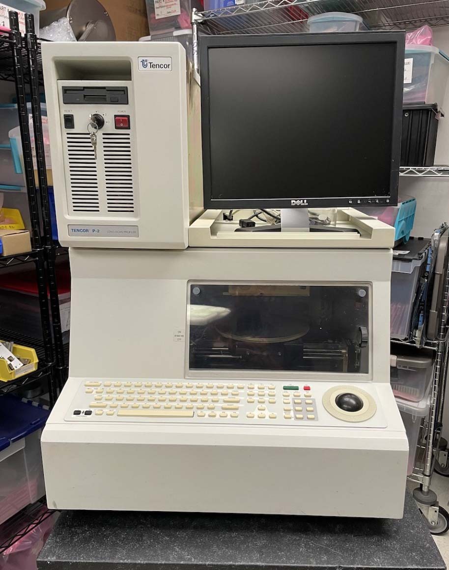
Used KLA / TENCOR P2 #9252431 for sale
It looks like this item has already been sold. Check similar products below or contact us and our experienced team will find it for you.
Tap to zoom


Sold
ID: 9252431
Surface profilers
Micro head
Sensor arm assembly
With 2.0 um stylus tip.
KLA / TENCOR P2 is a sophisticated wafer testing and metrology equipment that enables the characterization and visualization of a wafer's physical properties. This system has the capability to measure both light and darkfield images, providing detailed views of the wafer's topography over a wide range of magnifications. It also has the ability to analyze both atomic force and critical dimension, as well as the particulate defect level. KLA P-2 also includes a combined microscope/scanning electron microscope (SEM) chamber for supremely high resolution and high sensitivity inspections. The unit includes two primary metrology processes, Photon Scanning Tunneling Microscopy (PSTM) and Automated Shaped Defect Detections (ASDD). PSTM enables the most accurate analysis of the surface topology using a combination of tunneling electrical currents from the substrate surface and the laser beam emitted from the immersion optics. This also gives the microscope the highest resolution defection for the most precise imaging. On the other hand, ASDD processes allow for high speed automated detection of defects on both dark and bright areas. It is able to detected both shape and ligament defects for both large and small features. TENCOR P 2's unsurpassed uniformity of illumination in the darkfield mode inhibits background signal leakage onto the wafer, ensuring the highest detection throughput and the highest possible image contrast. It also features 4x to 128x mapping capabilities as well as MTF measurements to enable the most accurate characterization of the wafer. Moreover, as a modern wafer testing and metrology machine, KLA / TENCOR P 2 has the capability to perform thickness measurement without affecting electrical characteristics of the device. Further, the tool comprises of an Ergonomic User Interface (EUI). EUI allows for easier and automated data conversion and analysis, as well as simplified equipment operation and control. In addition, TENCOR P-2 has a number of integrated tools designed to help in the efficient analysis of the wafer and its component parts. The most important of these are the autofocus, the wafer stitching, the particle recognition, as well as the defect classification algorithms. TENCOR P2 is a premium class wafer testing and metrology systems in the semiconductor industry. Its combination of superior measurement and detection capabilities, automated data conversion and analysis, and range of powerful control tools, enable users to view, inspect and analyze their wafers with the highest precision and accuracy.
There are no reviews yet