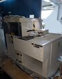
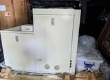
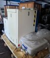
Used KLA / TENCOR P22 #293666311 for sale
URL successfully copied!
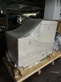
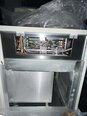
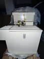
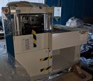
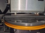
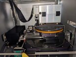
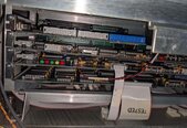
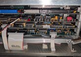
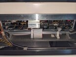
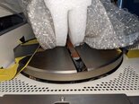
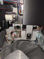
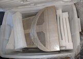
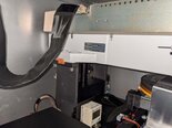
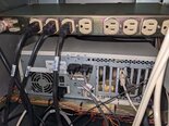
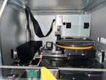

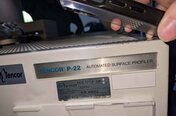
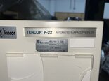
Tap to zoom
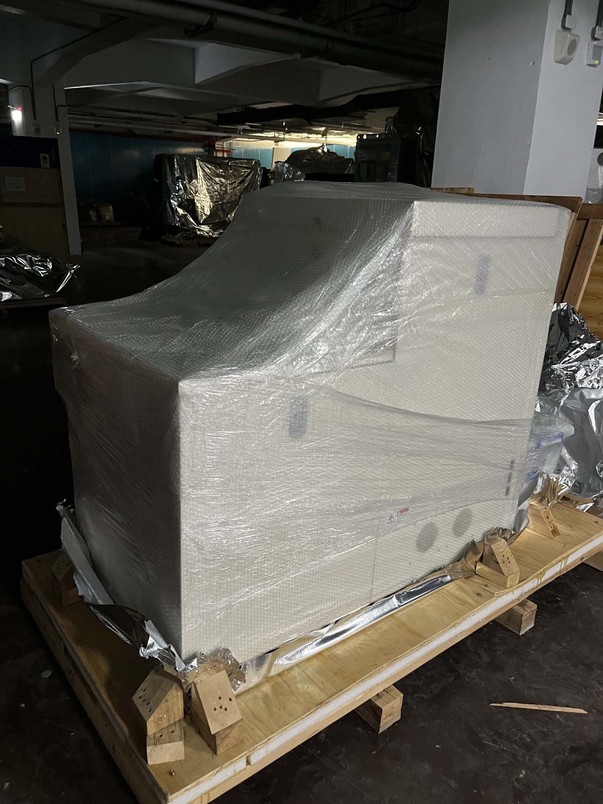

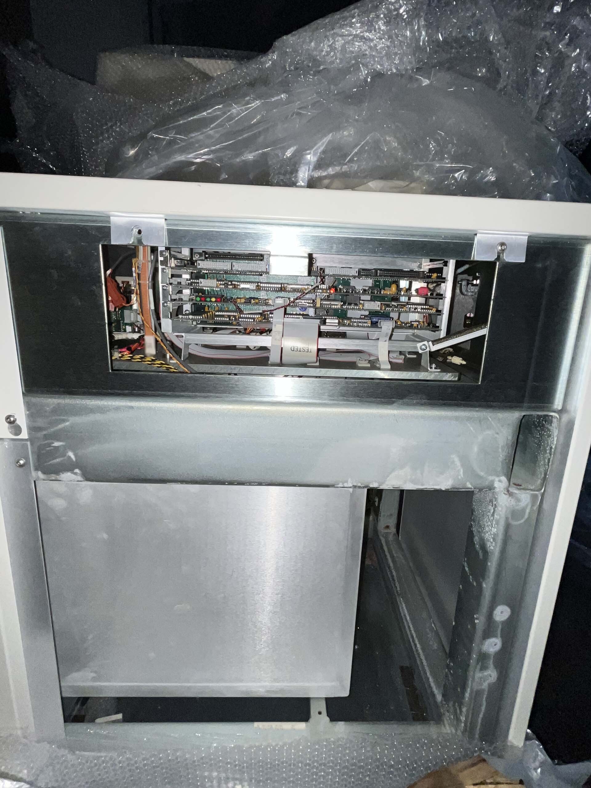
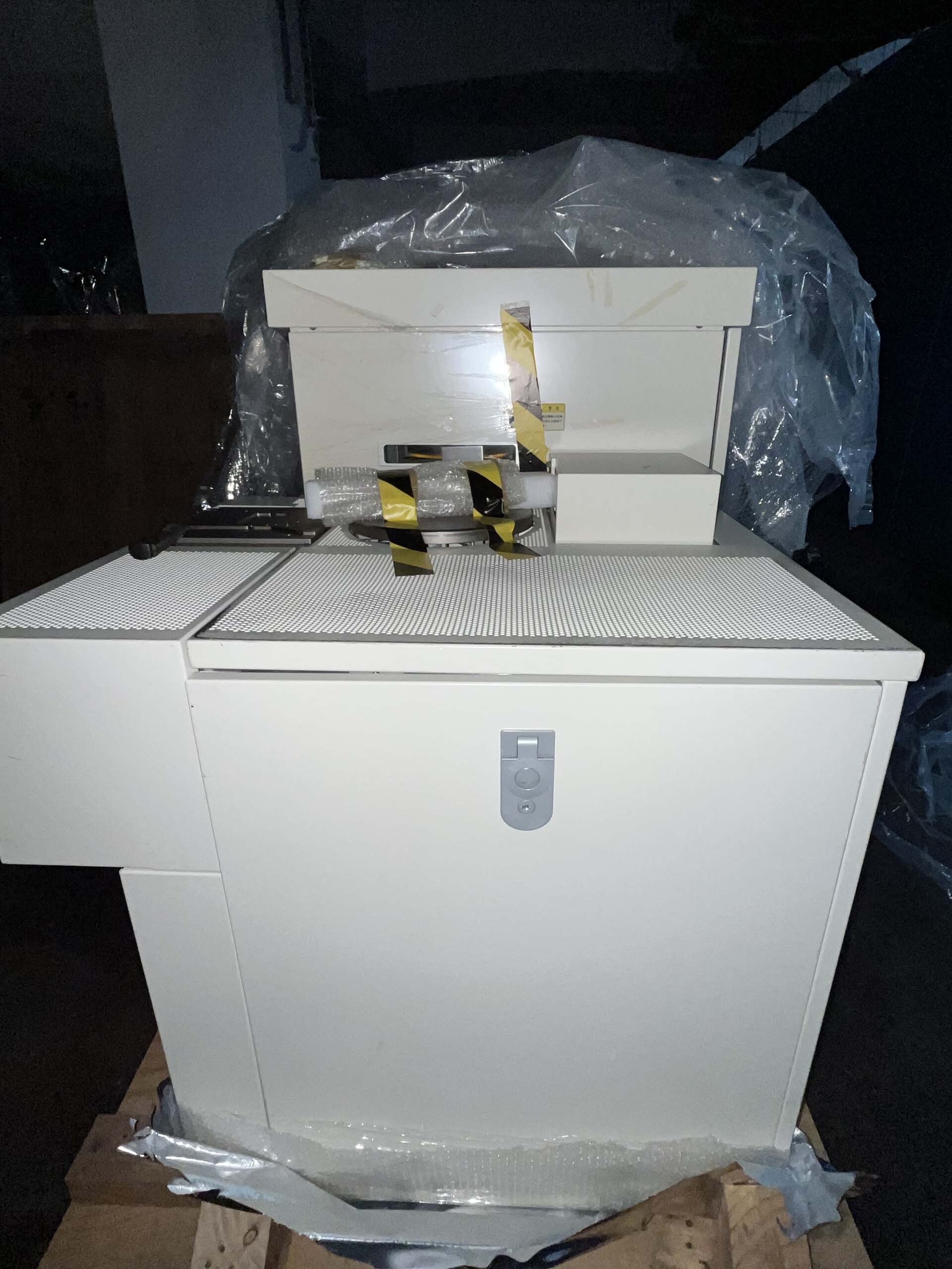
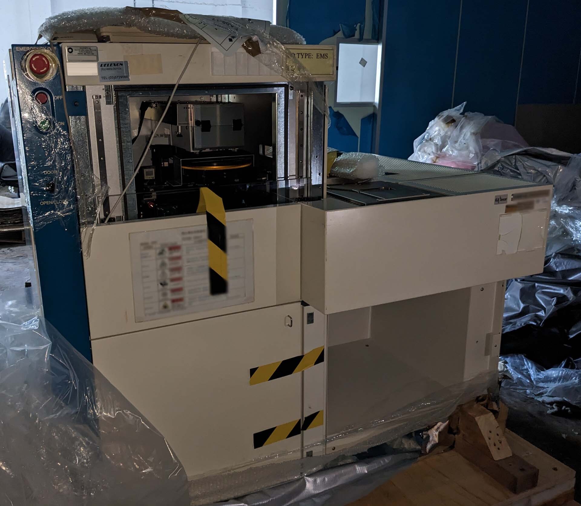
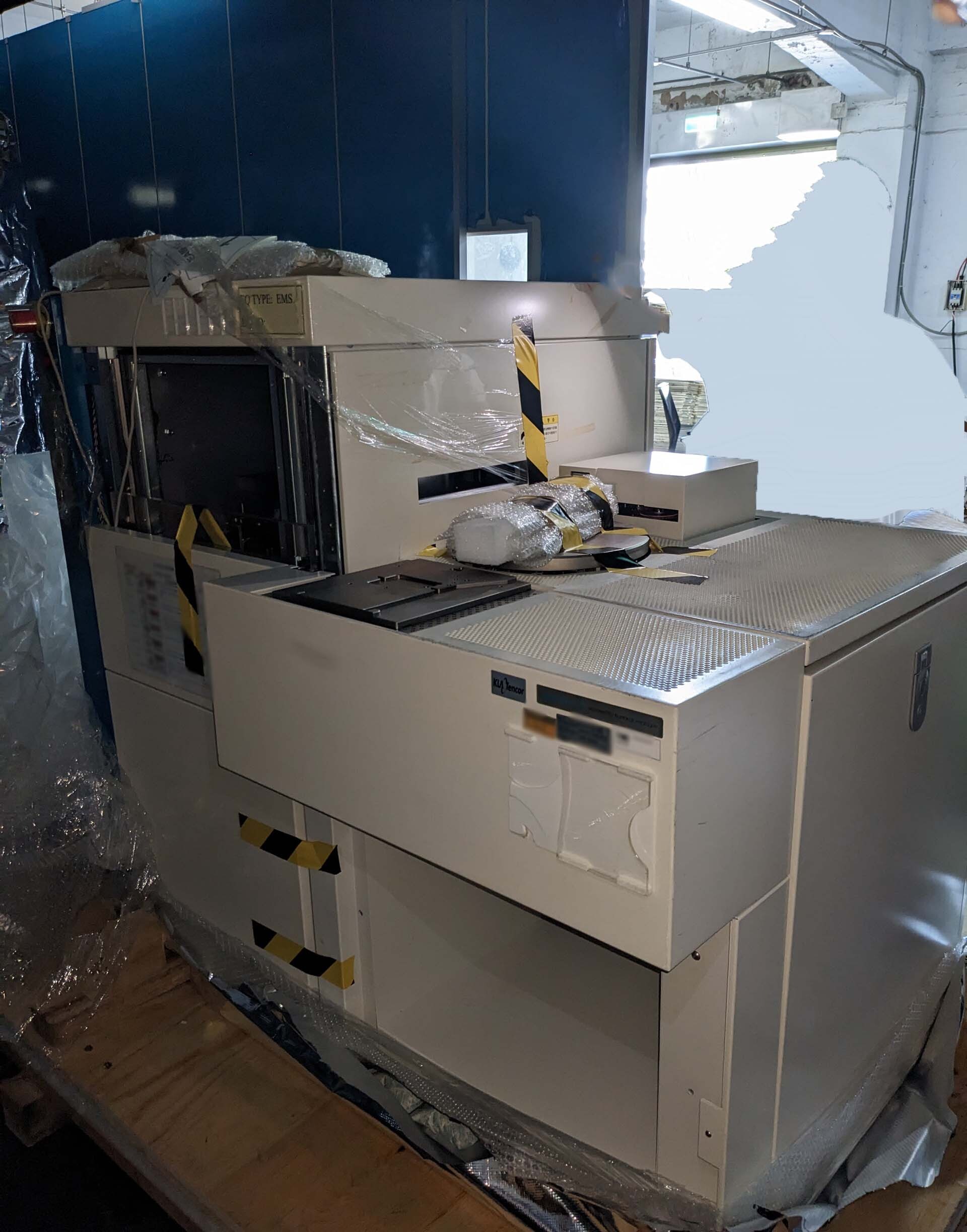
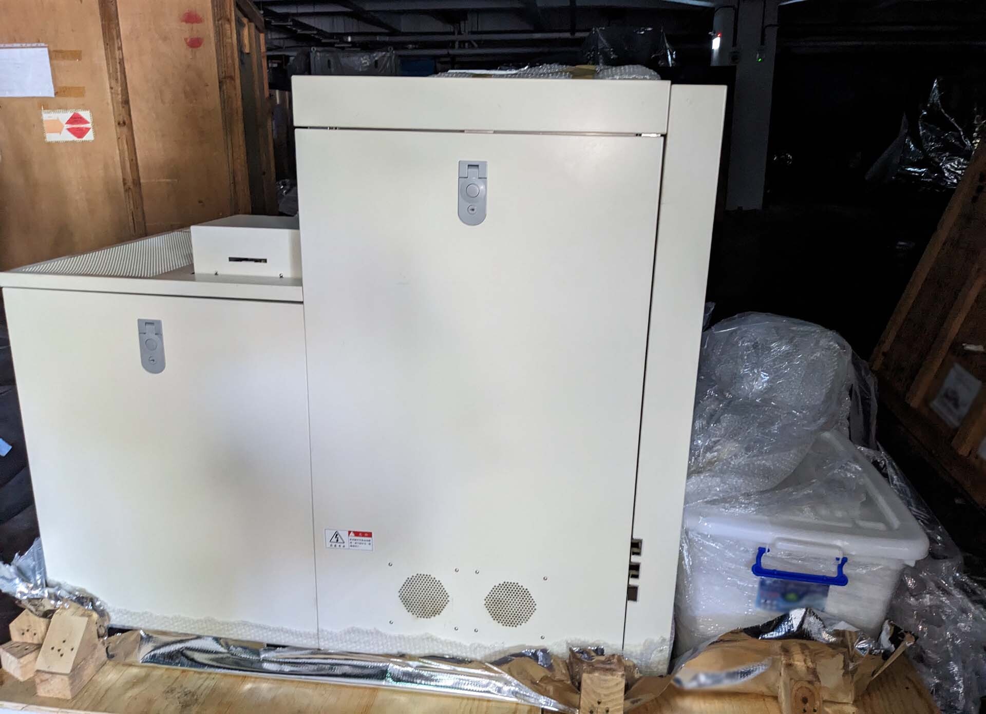
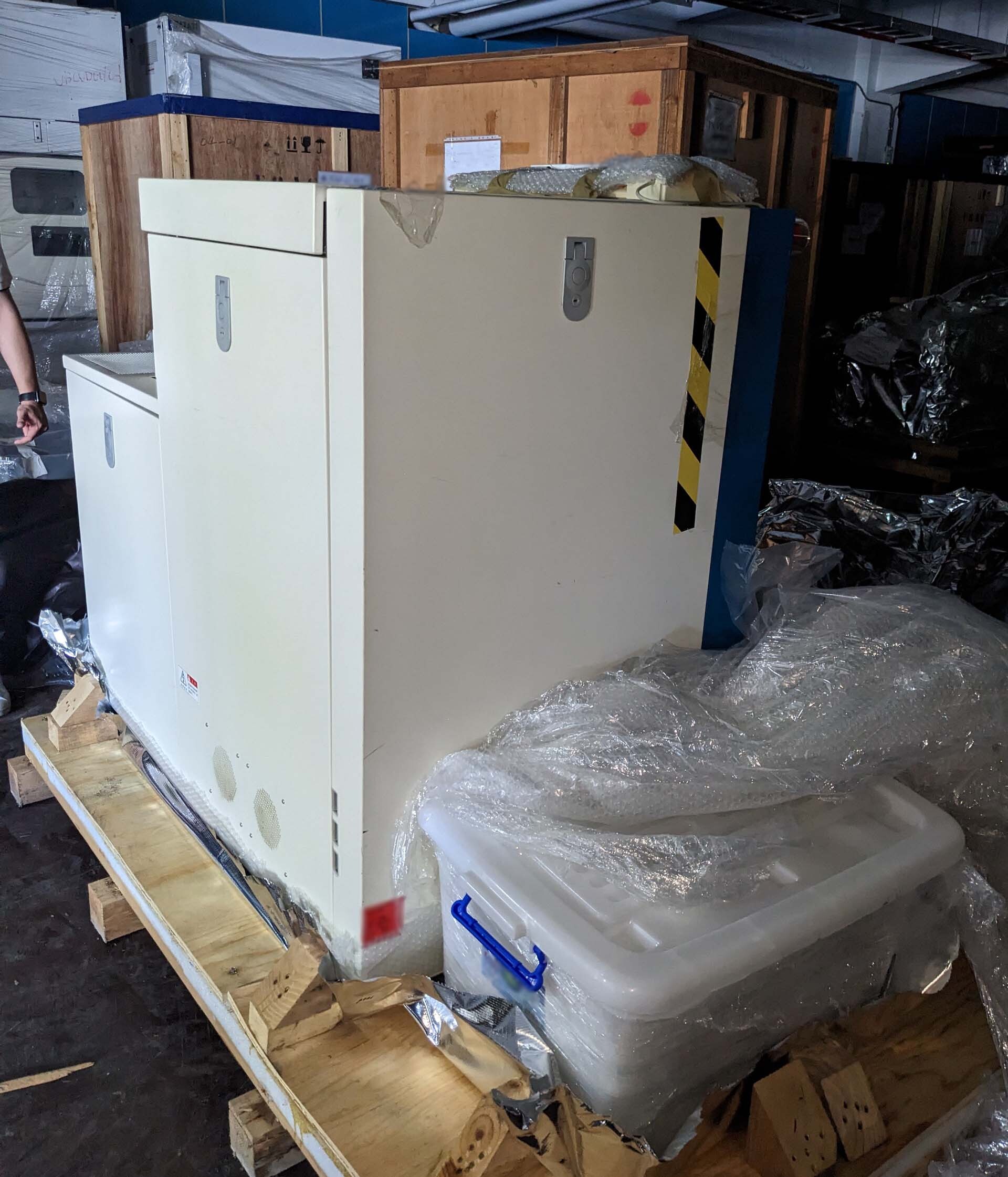
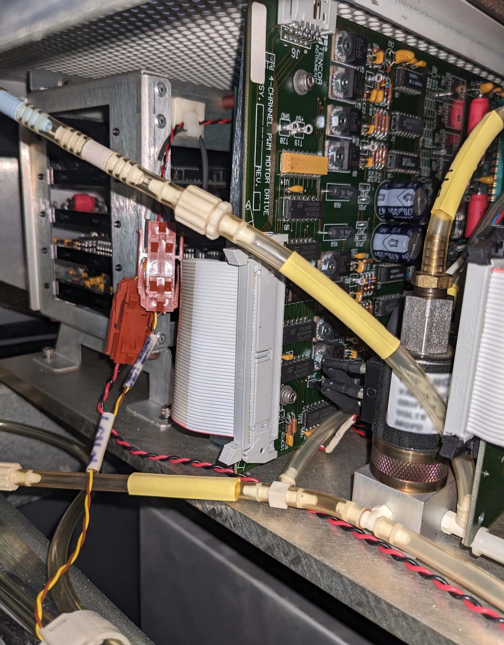
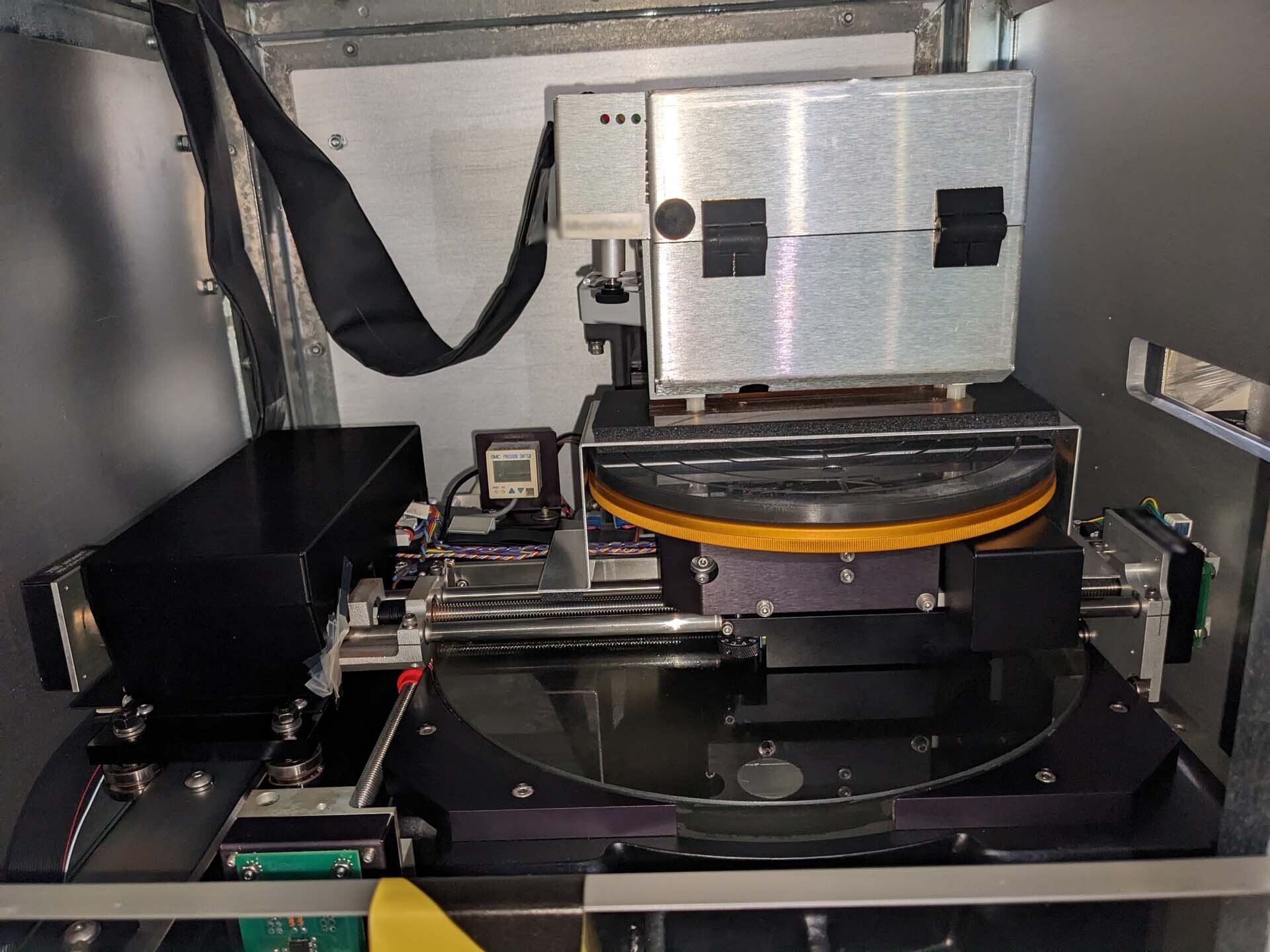
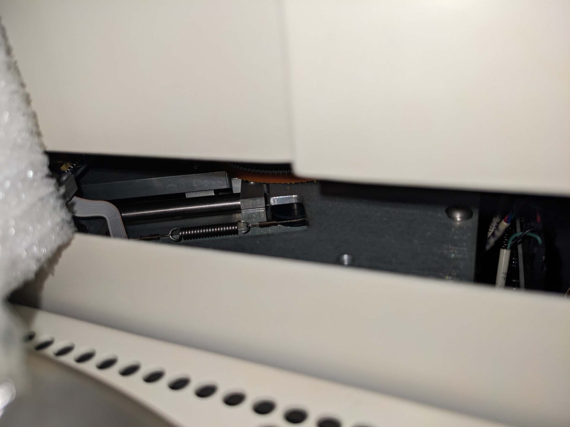
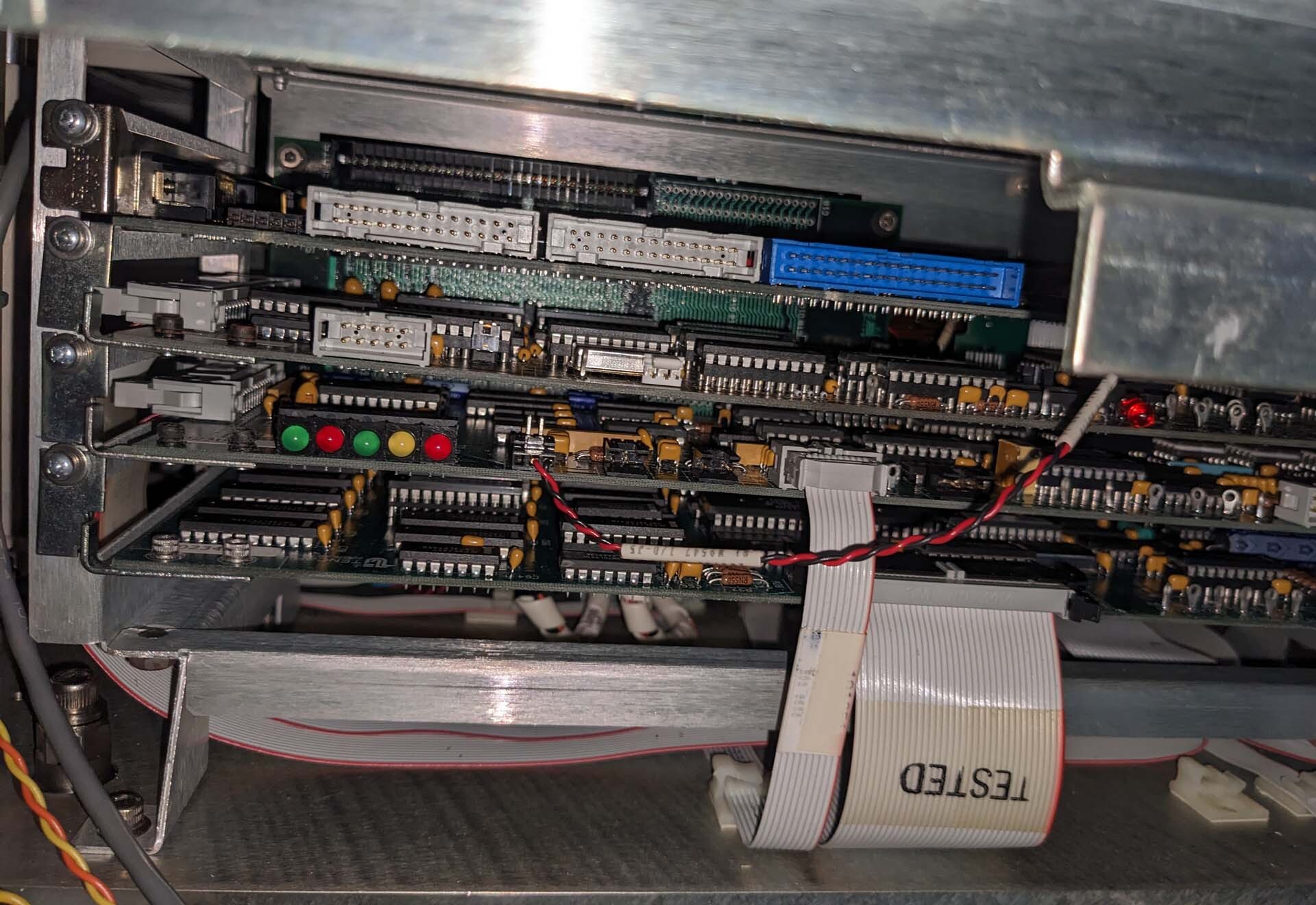
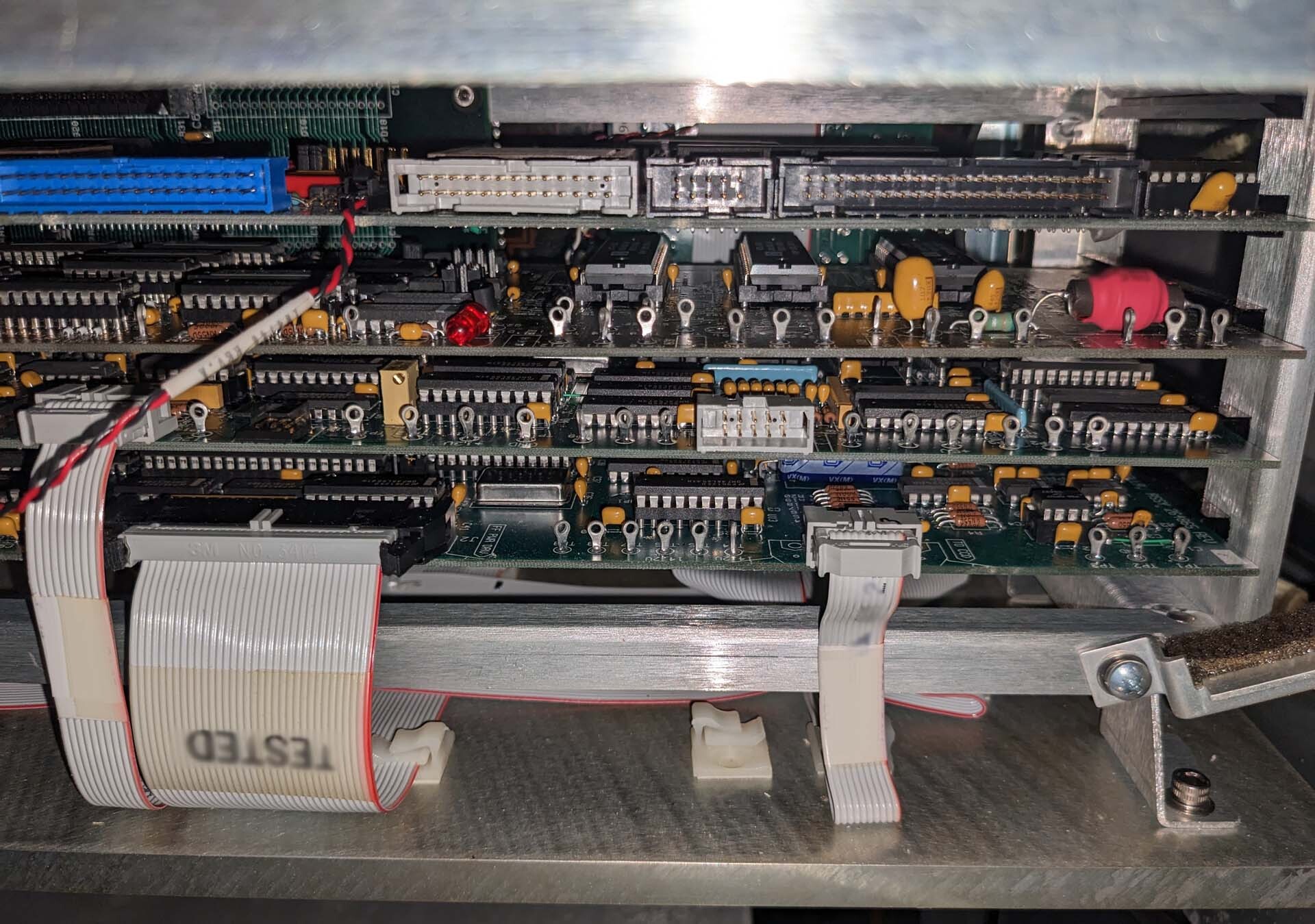
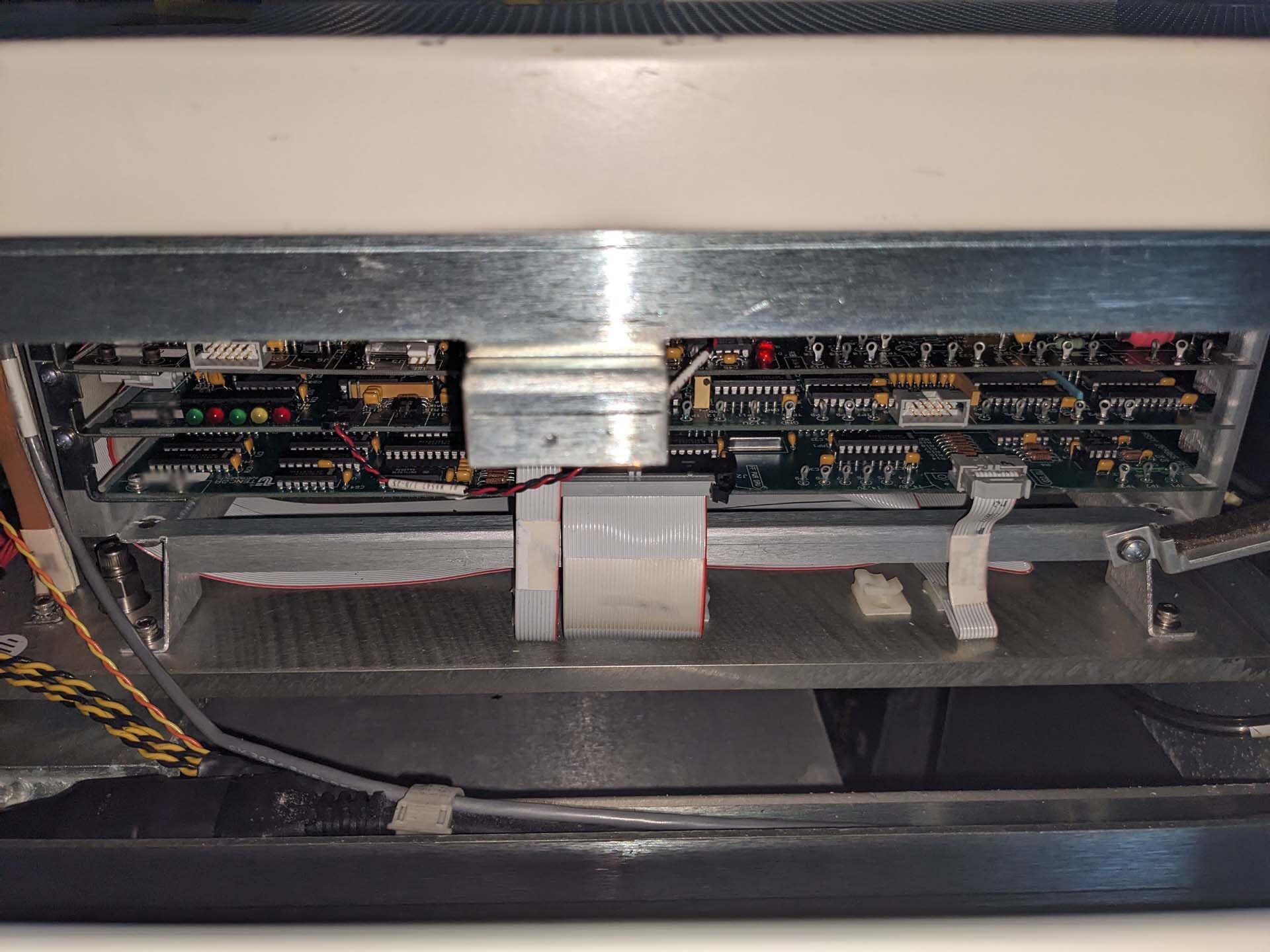
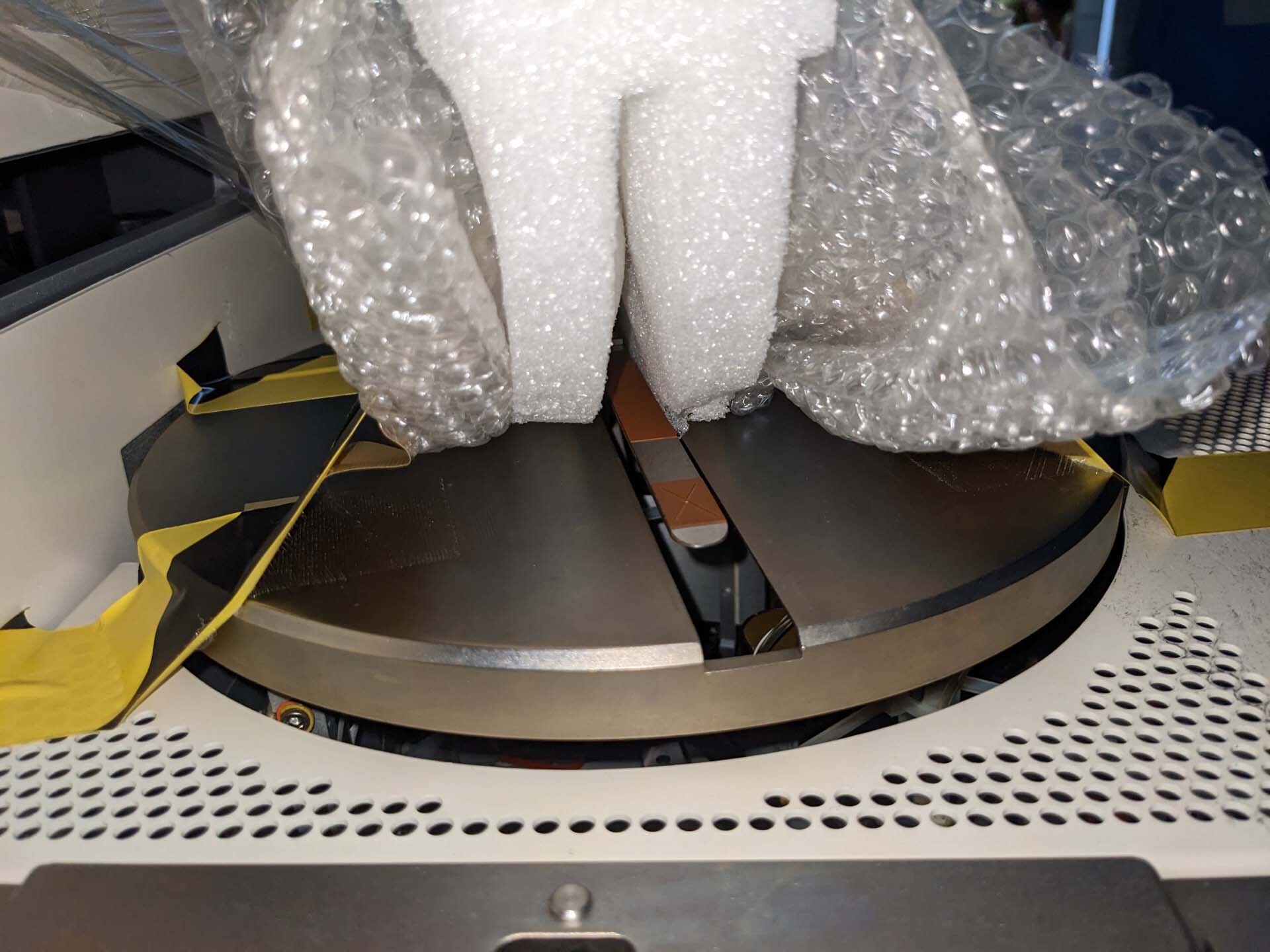
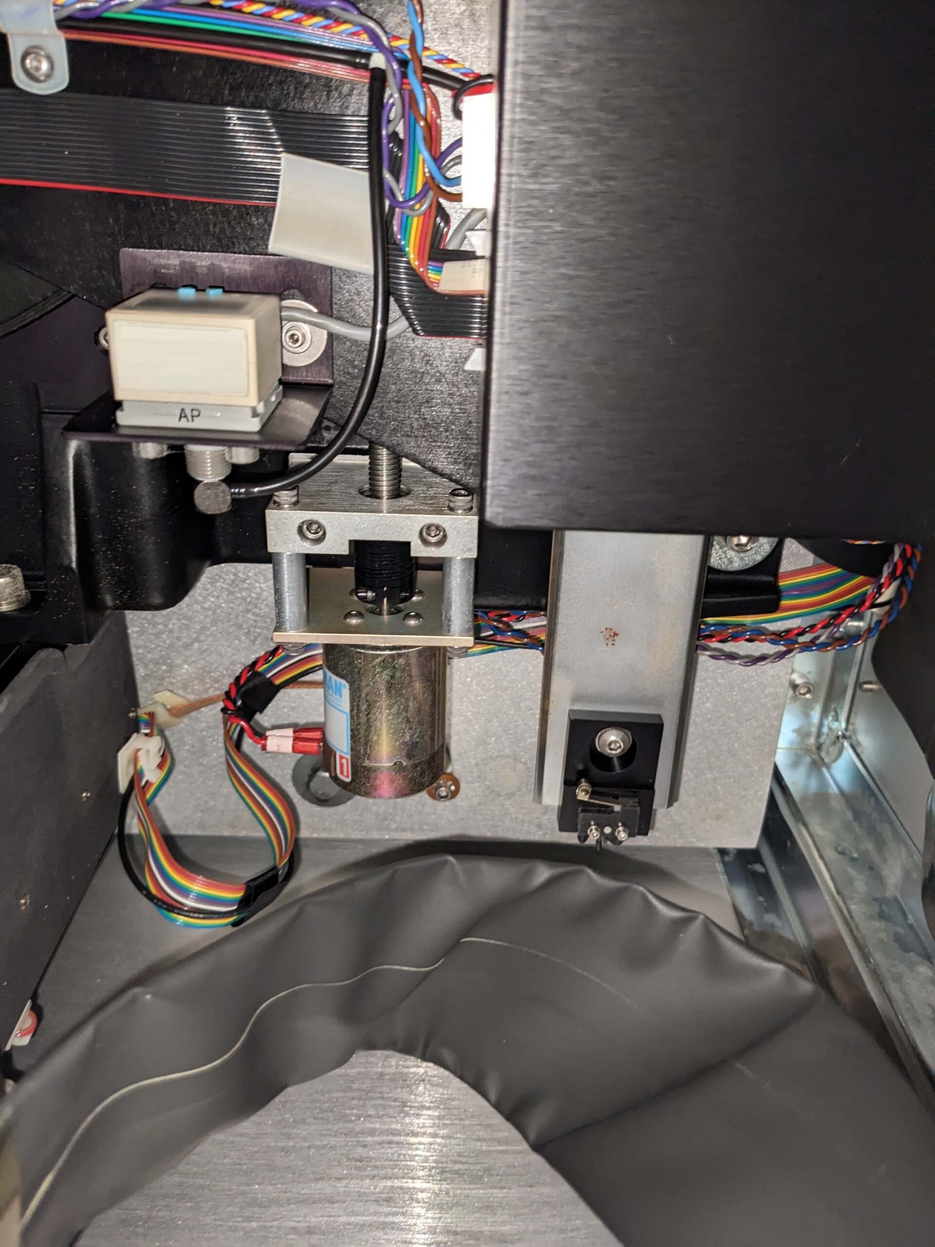
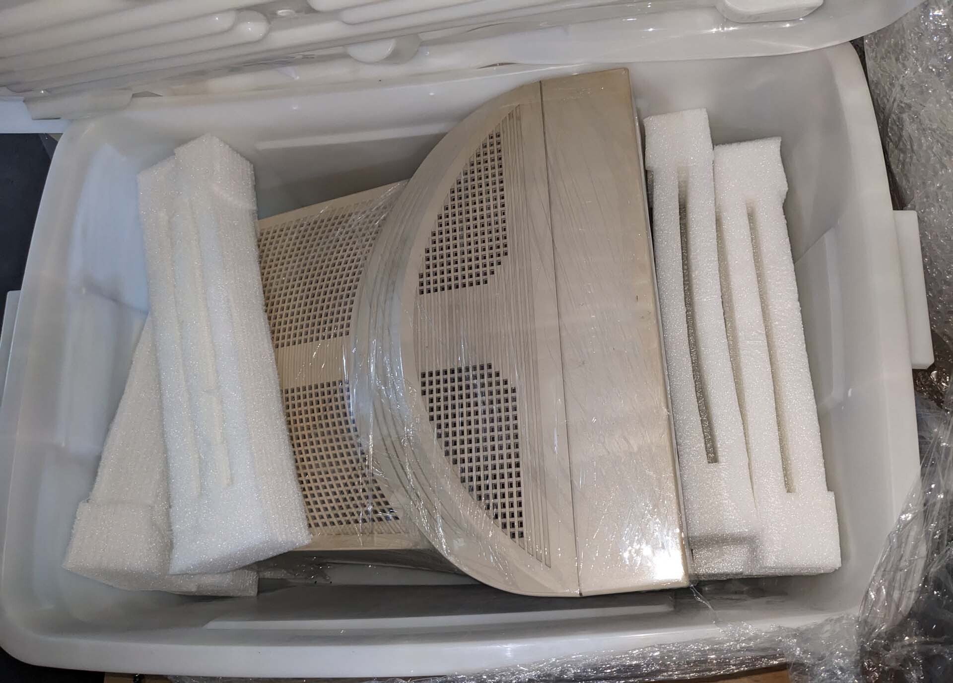
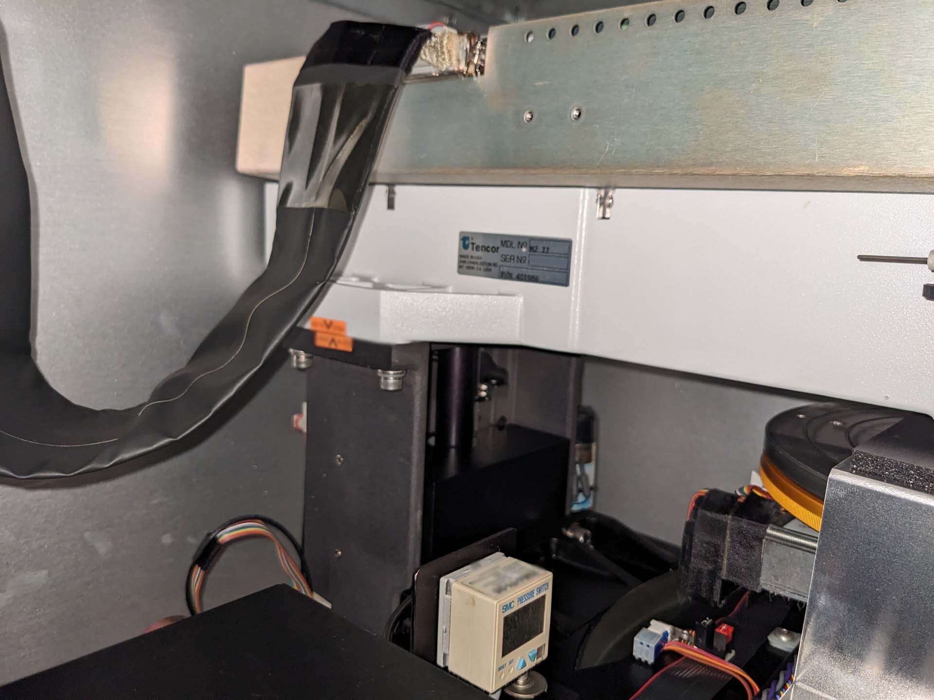
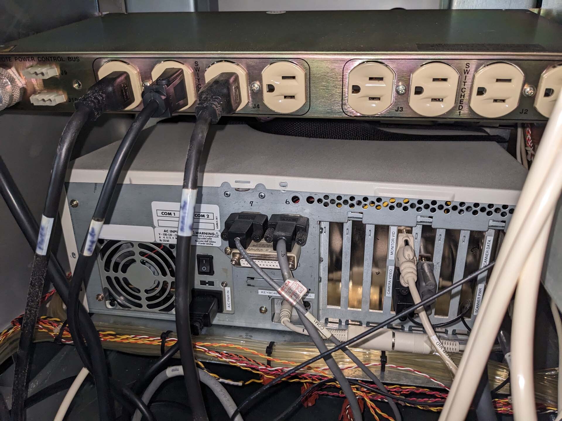
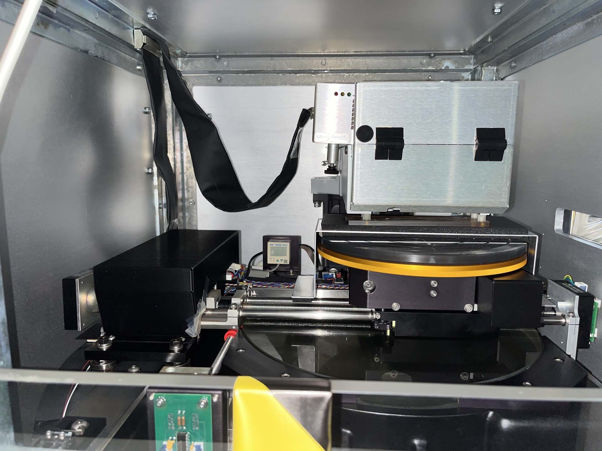

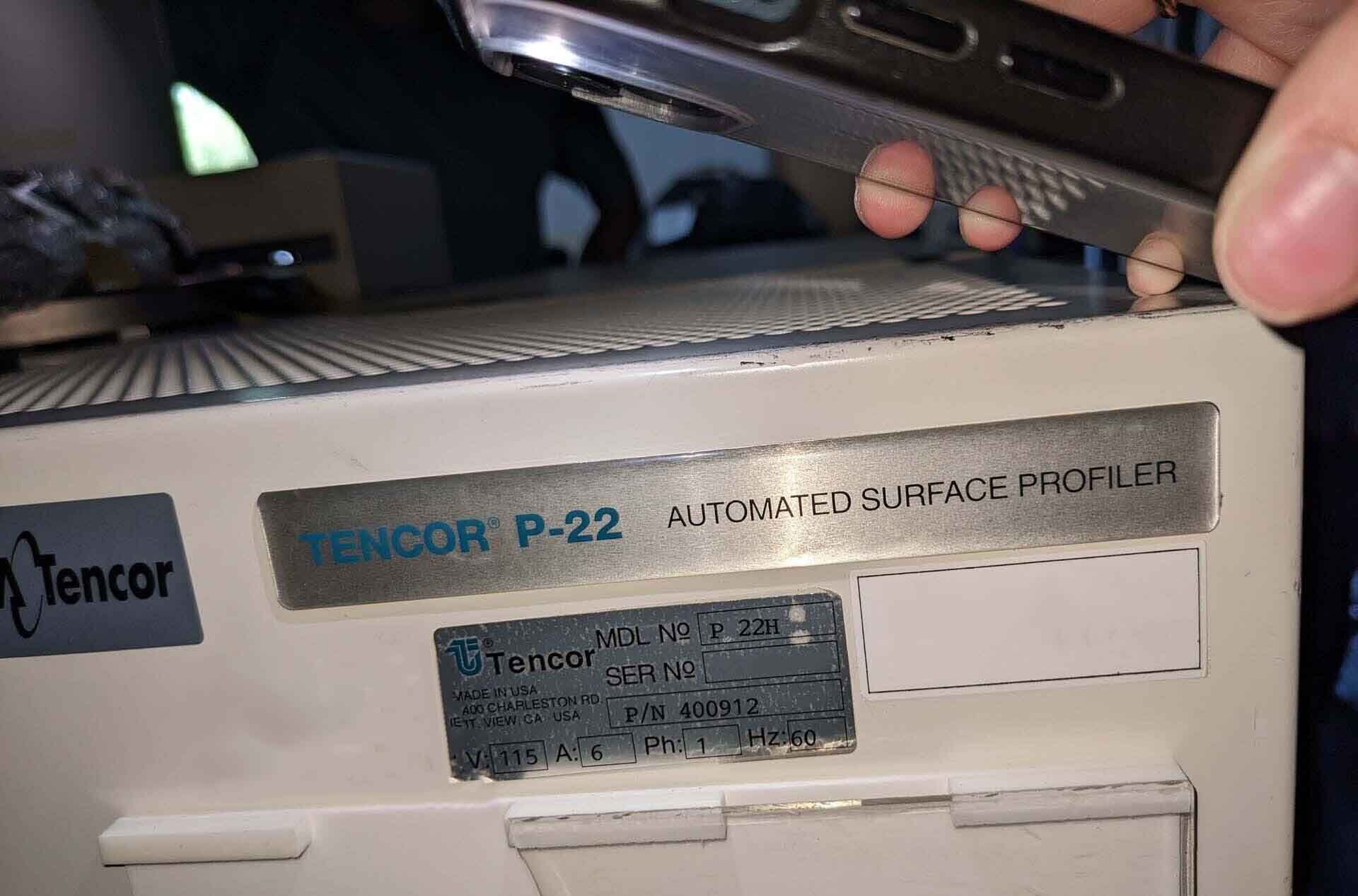
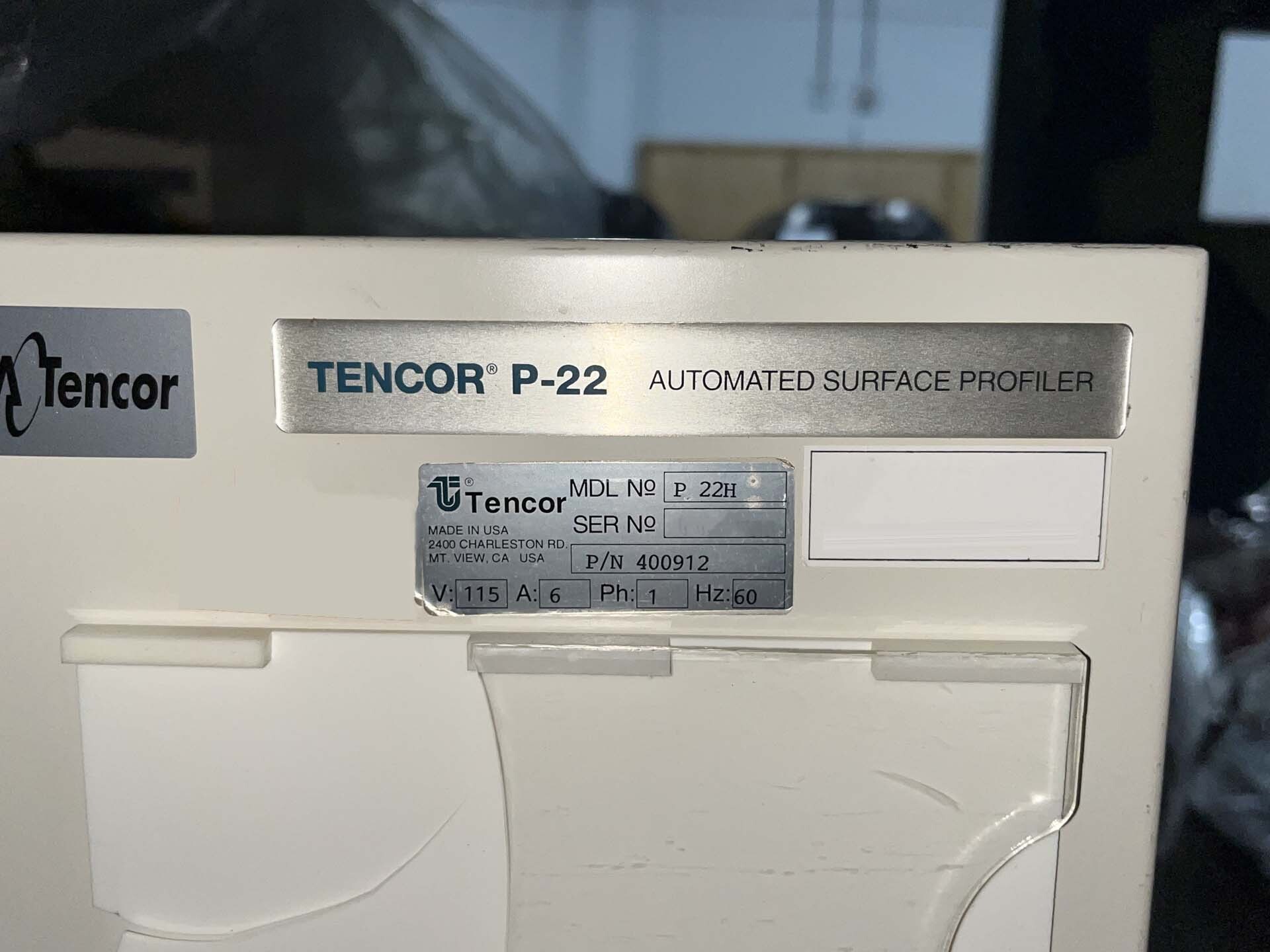
ID: 293666311
Wafer Size: 8"
Vintage: 1997
Surface profiler, 8"
P/N: 400912
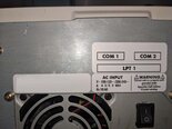
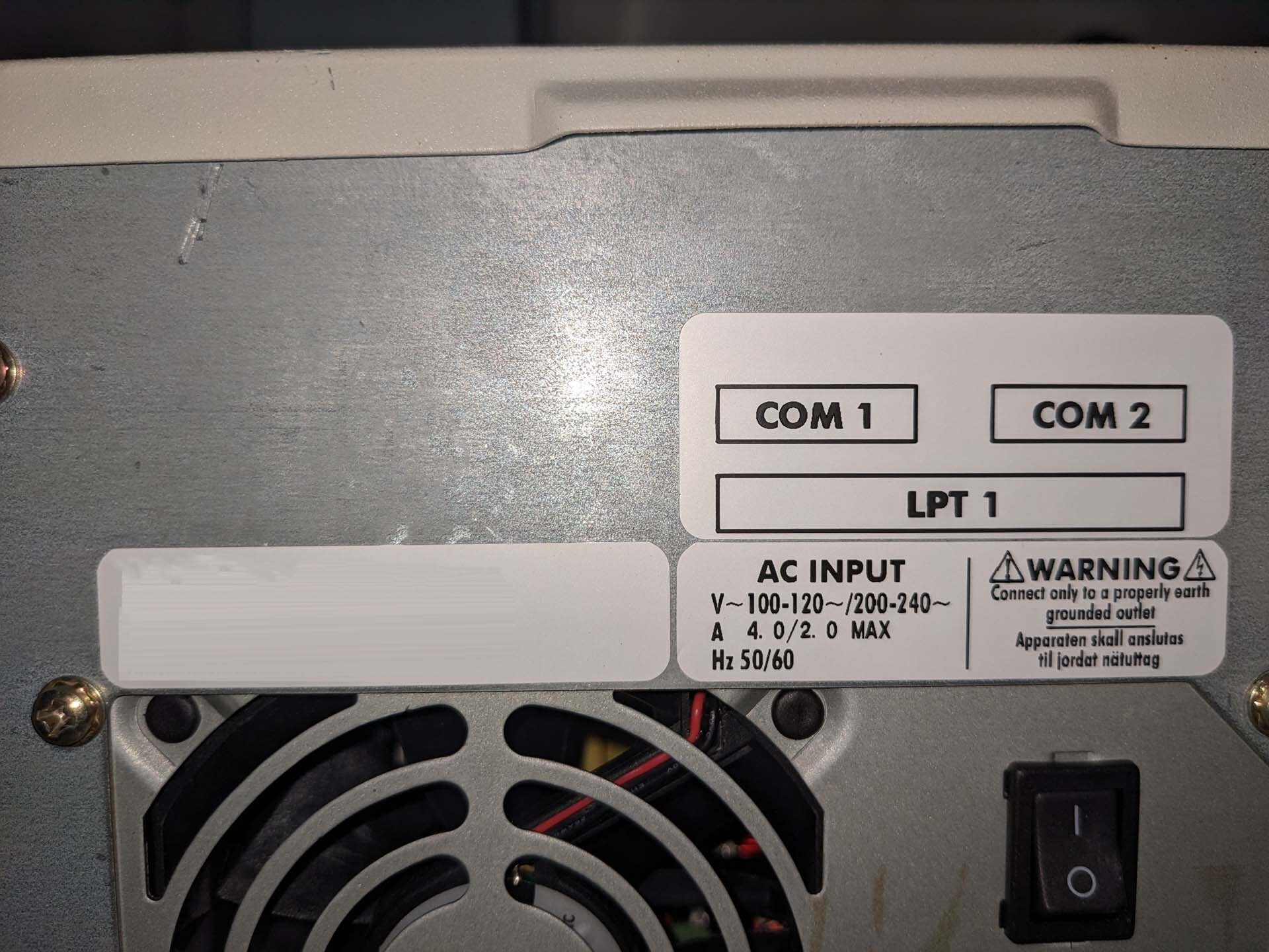
Power supply: 115 V, 6 A, Single phase, 60 Hz
1997 vintage.
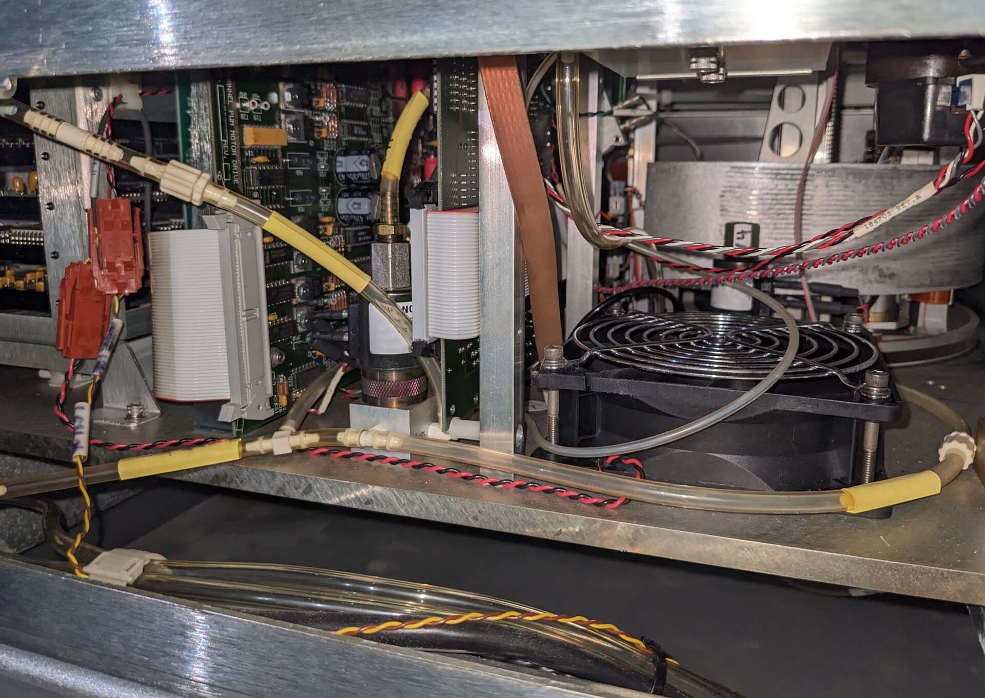
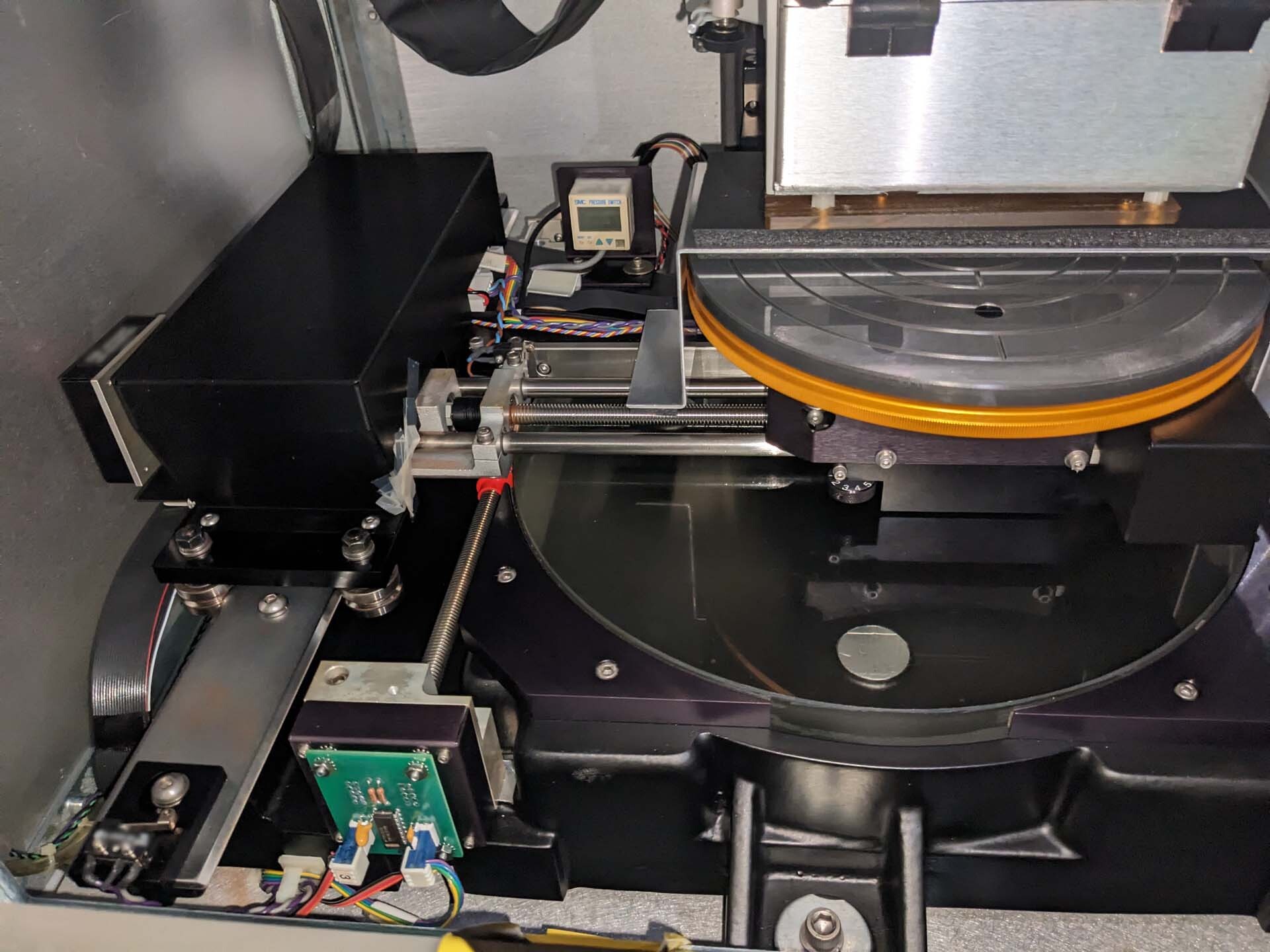
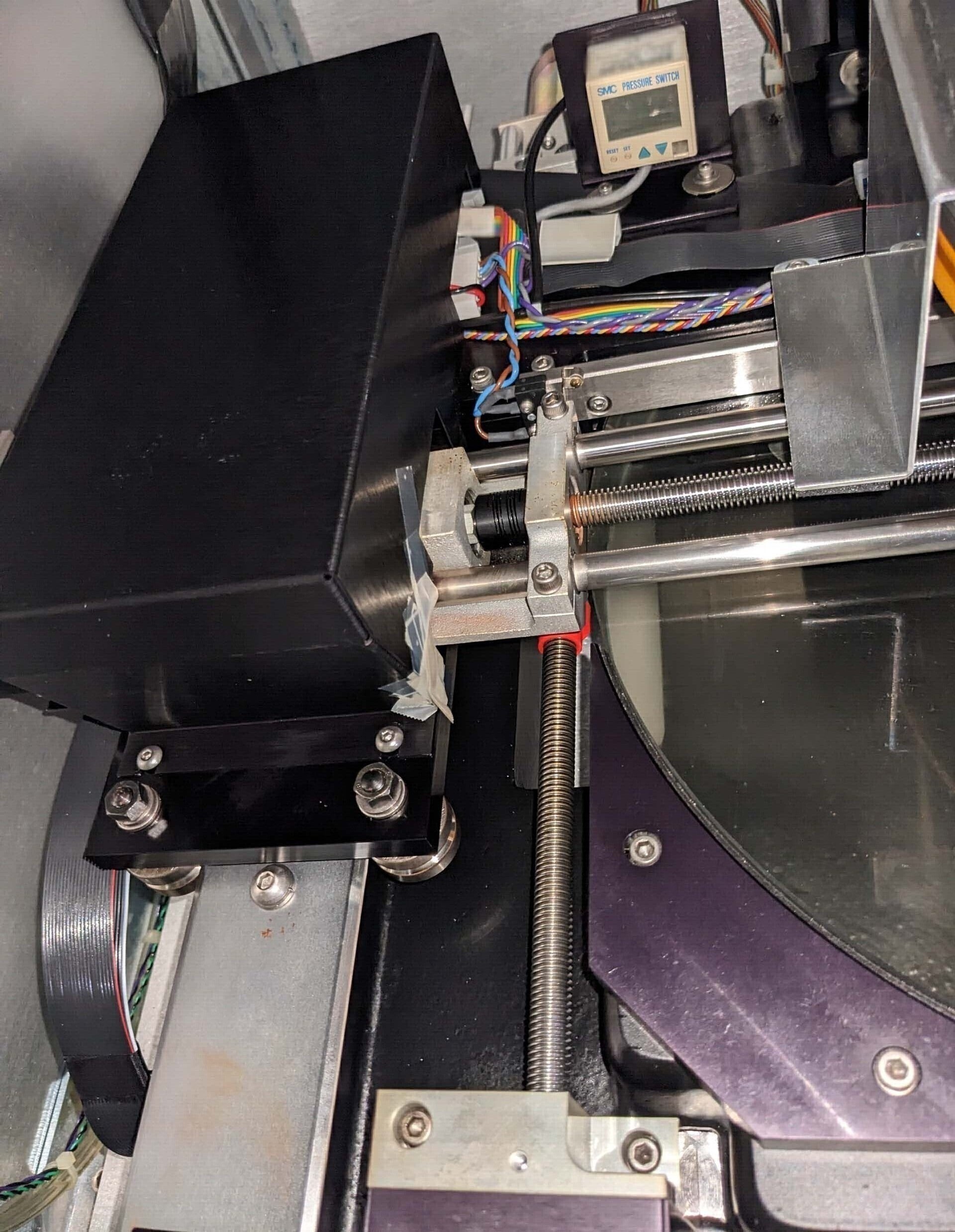
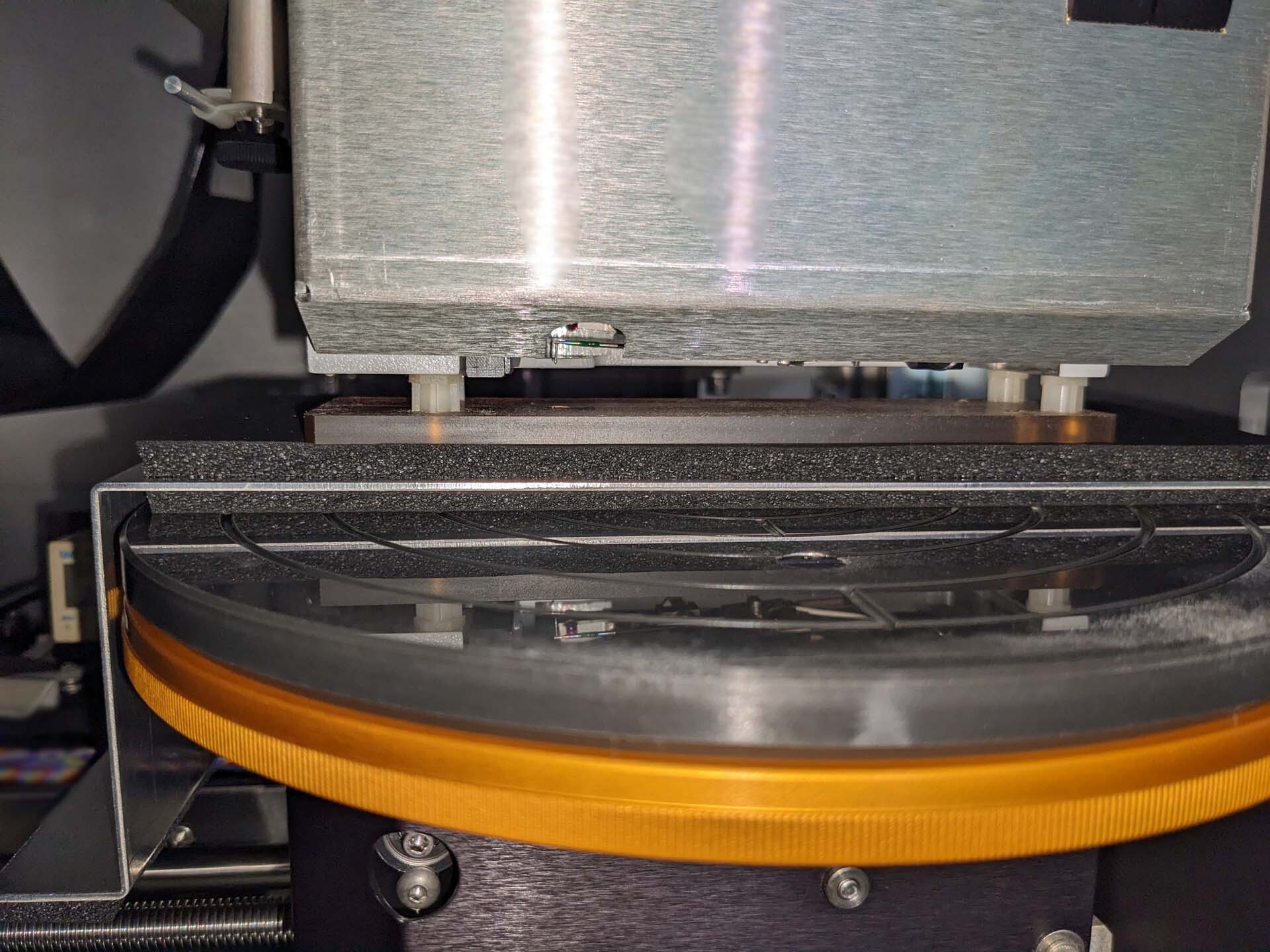
KLA / TENCOR P22 is a cutting-edge wafer testing and metrology equipment that plays a critical role in the semiconductor manufacturing process. As a crucial component of the semiconductor industry, KLA P 22 offers advanced capabilities for evaluating the quality and reliability of silicon wafers, ensuring that only the highest quality wafers are used in the production of integrated circuits. One of the key features of TENCOR P-22 is its ability to perform a wide range of measurements with exceptional accuracy and precision. The system utilizes sophisticated optical and laser-based technologies to analyze various parameters of the wafers, such as topography, roughness, film thickness, and defect detection. By providing comprehensive and detailed information about the wafer properties, TENCOR P22 enables manufacturers to optimize their production processes and enhance the overall yield and quality of semiconductor devices. The versatility of KLA P-22 is another notable aspect of this unit. It is capable of accommodating wafers of different sizes, ranging from small semiconductor wafers to larger display wafers, making it suitable for a variety of applications in the semiconductor industry. Additionally, P 22 can be easily configured to meet specific manufacturing requirements, allowing for flexibility and customization to suit different manufacturing processes and production lines. KLA / TENCOR P-22 is equipped with advanced software algorithms that enable efficient data analysis and visualization. The machine can generate detailed reports and actionable insights based on the measurements taken, facilitating decision-making and problem-solving in the semiconductor manufacturing environment. With its user-friendly interface and intuitive controls, operators can easily navigate the tool and extract valuable information from the data acquired, streamlining the testing and metrology process. In addition to its measurement capabilities, TENCOR P 22 is designed to enhance productivity and throughput in semiconductor manufacturing facilities. The asset features automated handling and wafer mapping functions, enabling rapid and efficient processing of wafers without compromising accuracy or repeatability. This automation reduces the risk of human error and ensures consistent results, ultimately leading to increased efficiency and cost-effectiveness for semiconductor manufacturers. Furthermore, P22 incorporates advanced wafer tracking and traceability features to ensure the integrity and quality of the semiconductor production process. By maintaining a detailed record of each wafer's measurements and history, the model enables comprehensive data management and quality control, helping manufacturers to identify and address any issues that may arise during wafer testing and metrology. Overall, KLA P22 represents a state-of-the-art solution for wafer testing and metrology in the semiconductor industry. With its advanced capabilities, versatile design, and user-friendly interface, KLA / TENCOR P 22 provides manufacturers with a powerful tool for optimizing their semiconductor production processes and delivering high-quality, reliable semiconductor products to the market. By investing in P-22, semiconductor manufacturers can achieve greater efficiency, productivity, and quality in their operations, ultimately ensuring their competitive edge in the dynamic semiconductor market.
There are no reviews yet