Used KLA / TENCOR P2H #293758331 for sale
URL successfully copied!

Tap to zoom
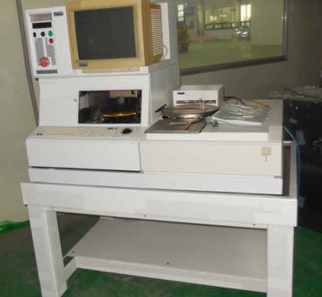

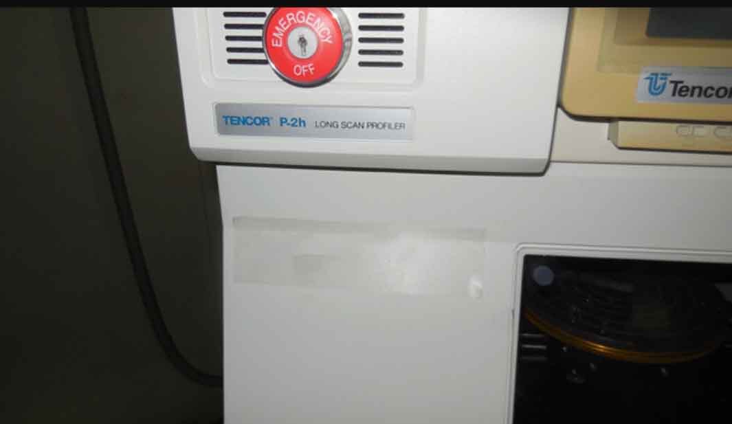
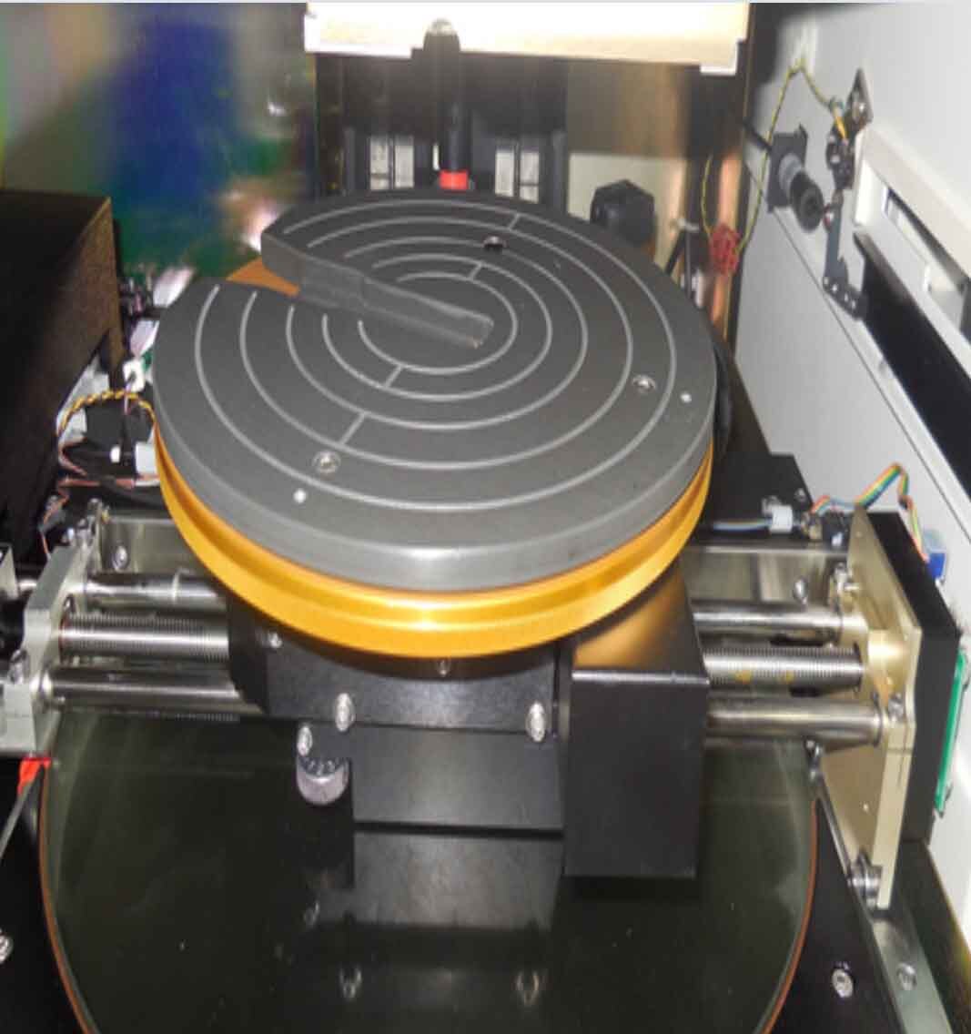
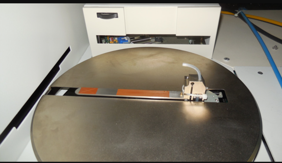
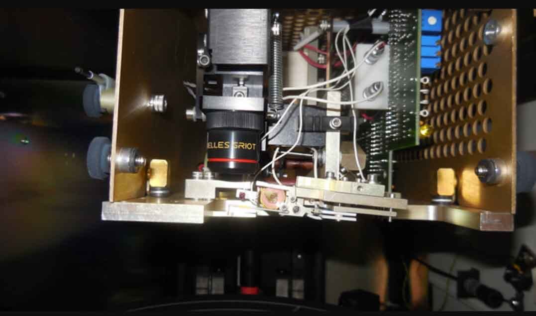
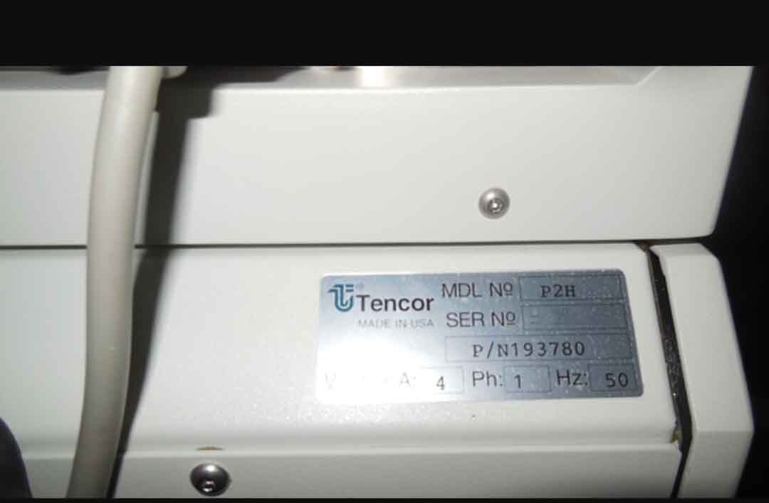
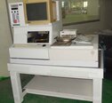
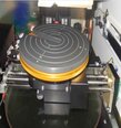
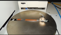
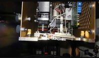
KLA / TENCOR P2H is an advanced wafer testing and metrology equipment designed for high throughput and performance. It uses an image acquisition system and an image processing unit as well as a host of other components to analyze and characterize semiconductor devices on a wafer. It is used to meet stringent process control requirements for advanced semiconductor devices such as finFETs, 3D NANDs, and others. The image acquisition machine of KLA P-2H has a peak tool resolution of 0.05 µm, allowing it to deliver highly accurate and reliable process control across the entire wafer surface. Its automated surface sensing feature allows the asset to acquire images of each die on the wafer at up to two images per second, significantly increasing throughput and providing accurate characterization. The image processing model of TENCOR P 2H consists of advanced algorithms that enable it to quickly identify defects, measure critical features, and compare actual performance with the expected performance. This enables the equipment to make accurate defect recognition and process assessment, and to provide feedback to the manufacturing process to ensure high yields and process optimization. KLA / TENCOR P 2H also includes a software control suite to help users visualize complex process data. It provides an intuitive graphical user interface (GUI) that enables effective process control of the system, as well as enabling efficient data sharing across the manufacturing process. The unit is also equipped with the ability to improve yield and process control analytics, allowing it to detect potential process issues. TENCOR P 2 H wafer testing and metrology machine is a highly advanced solution designed to meet the needs of high-performance semiconductor device manufacturers. It offers a comprehensive suite of image acquisition, image processing, and software control functionality, providing an effective solution for process control across a variety of device types. It not only provides accurate characterization and defect recognition capabilities, but also enables efficient data sharing and improved yield and process optimization analytics. As such, it is an ideal solution for the demanding needs of advanced semiconductor device manufacturers.
There are no reviews yet