Used KLA / TENCOR PHX DF 2.0 #293793609 for sale
URL successfully copied!


Tap to zoom
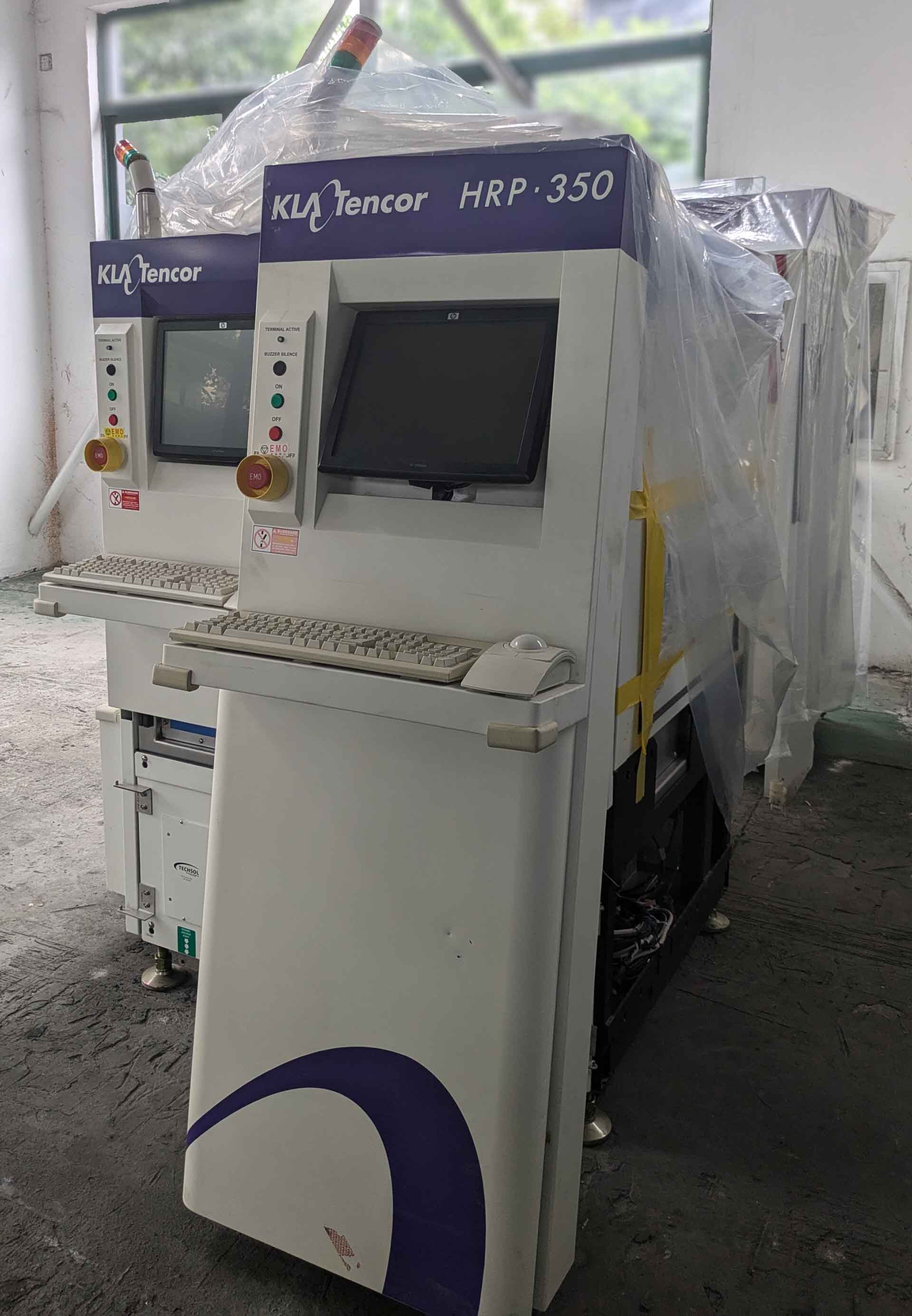

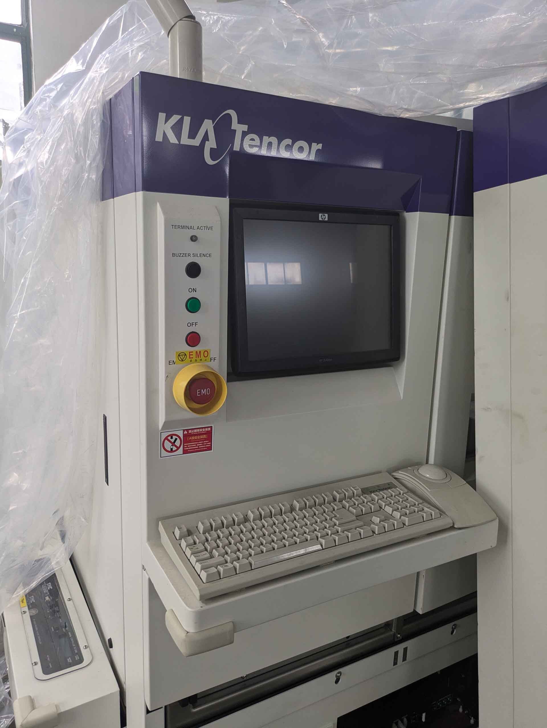
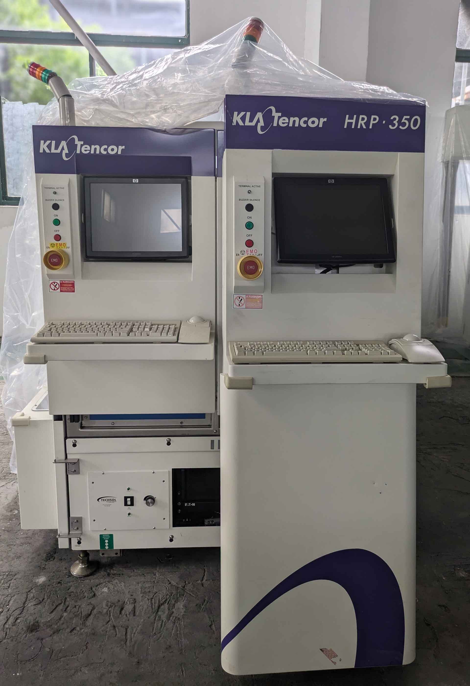
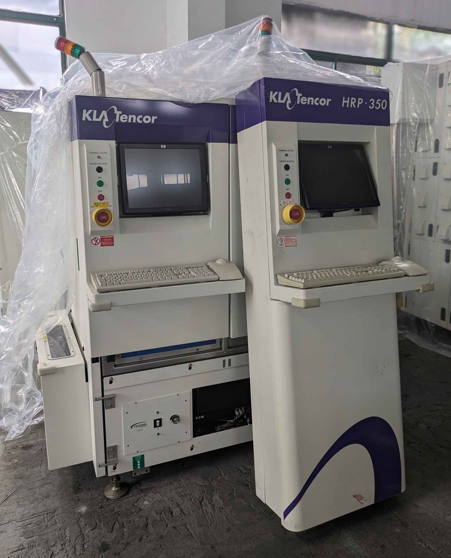
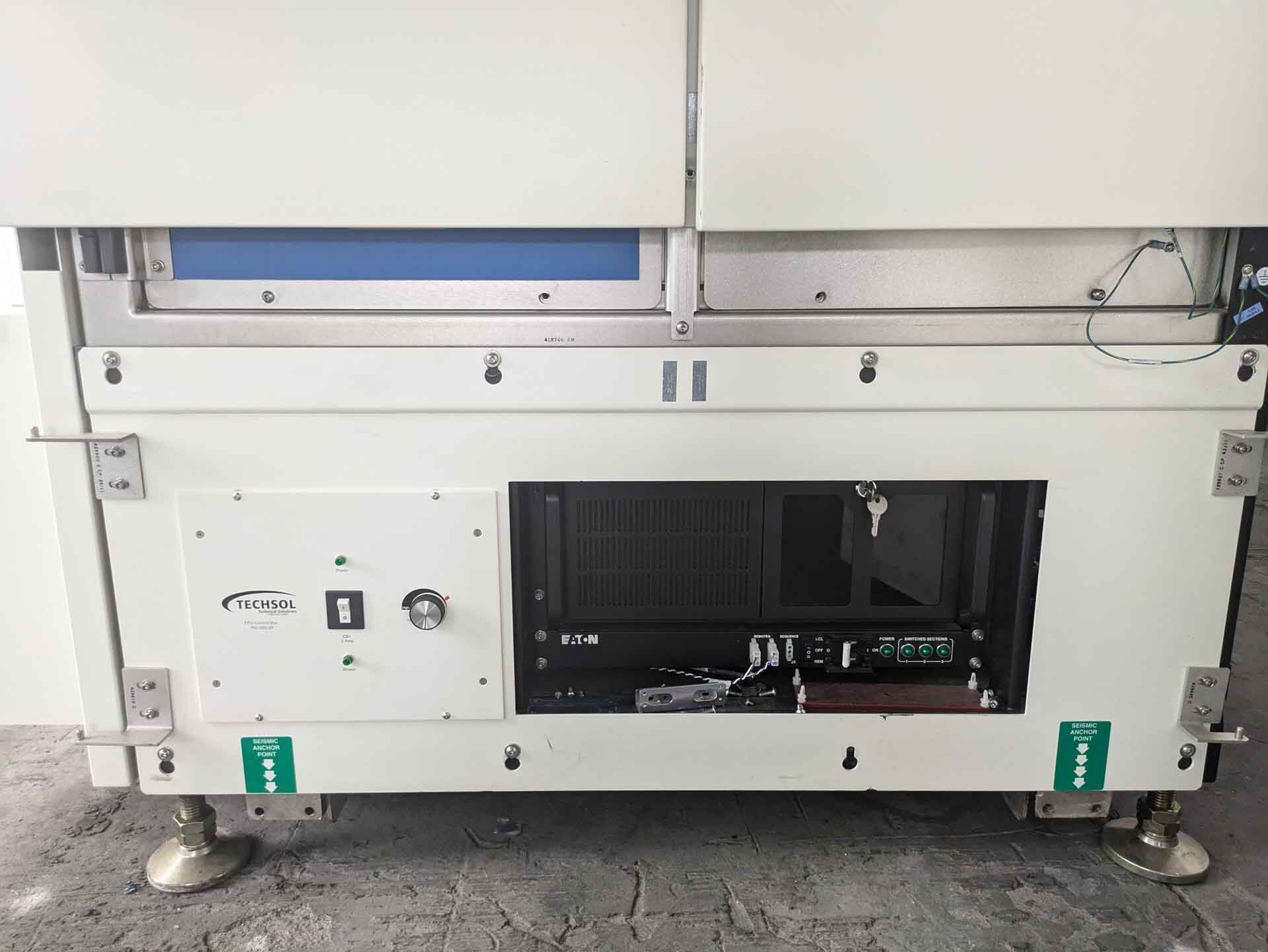
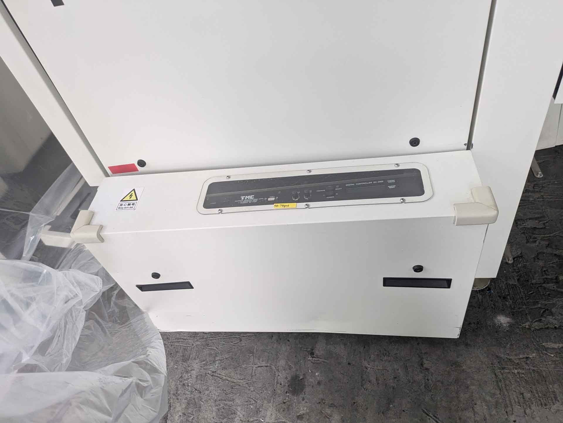
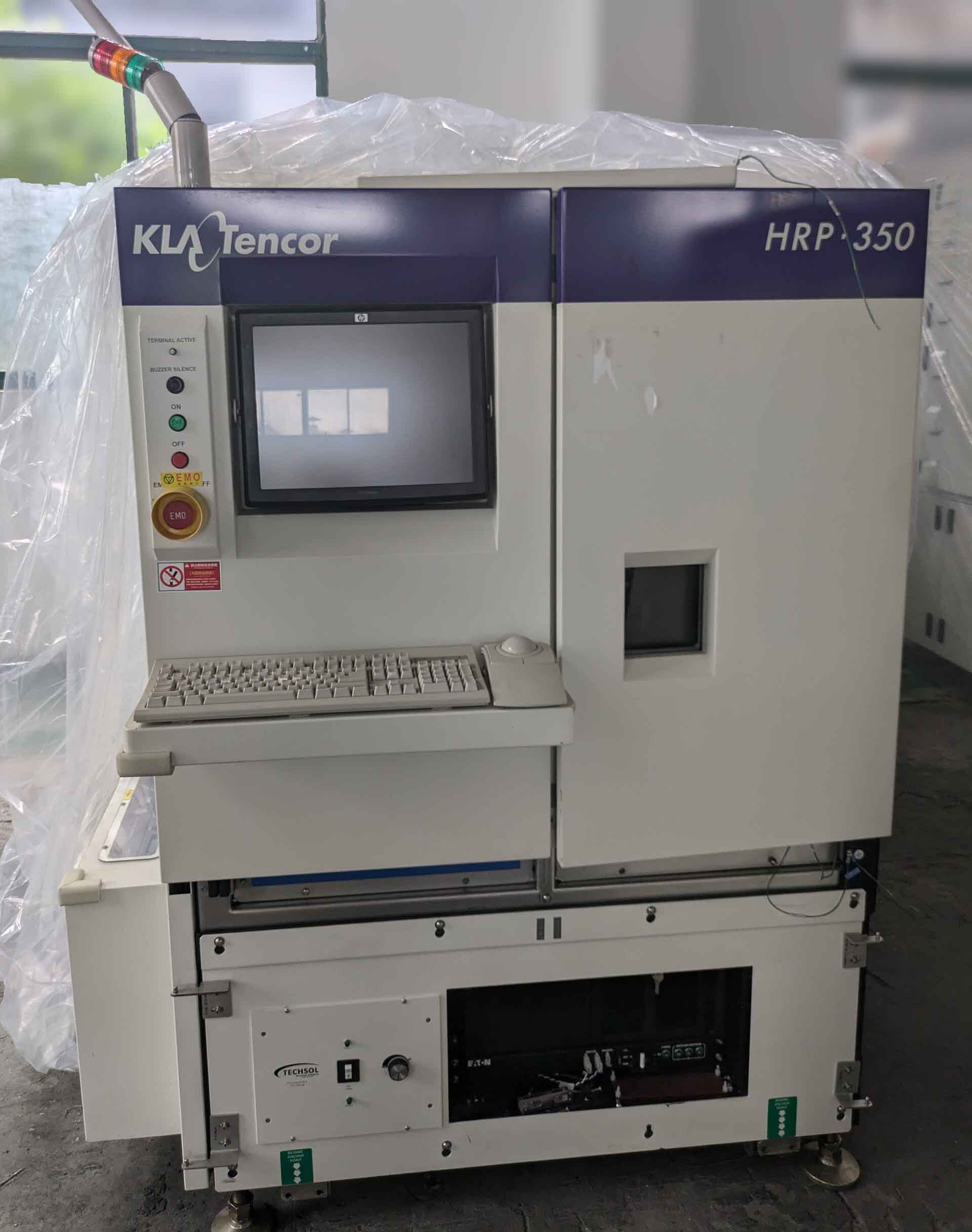
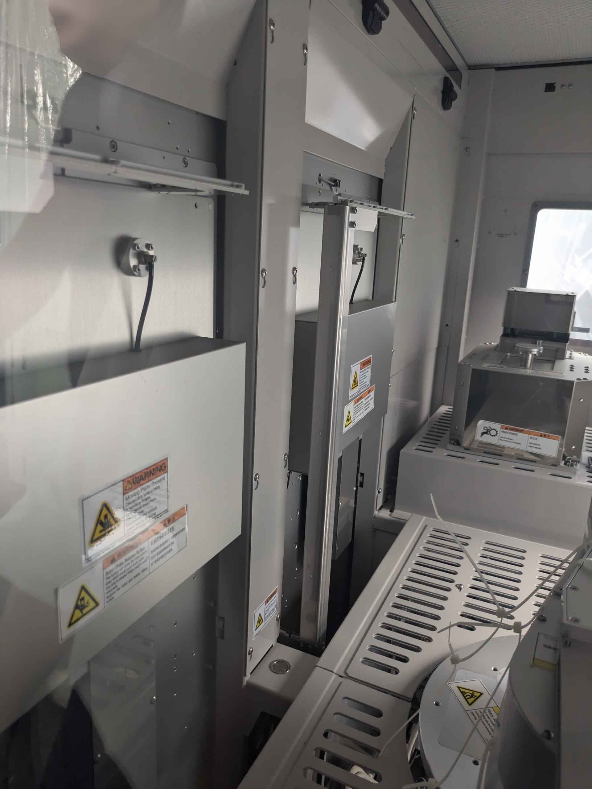
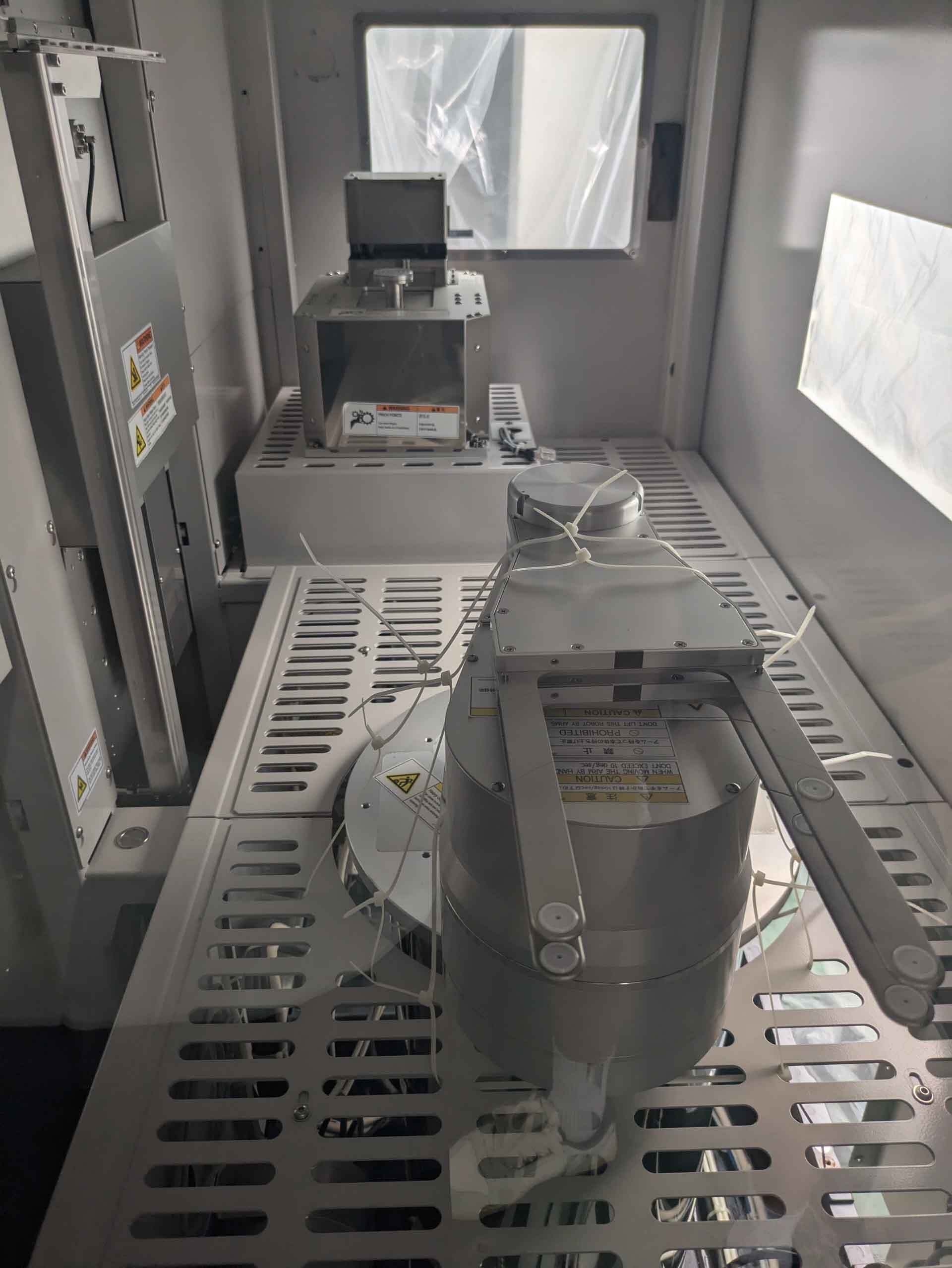
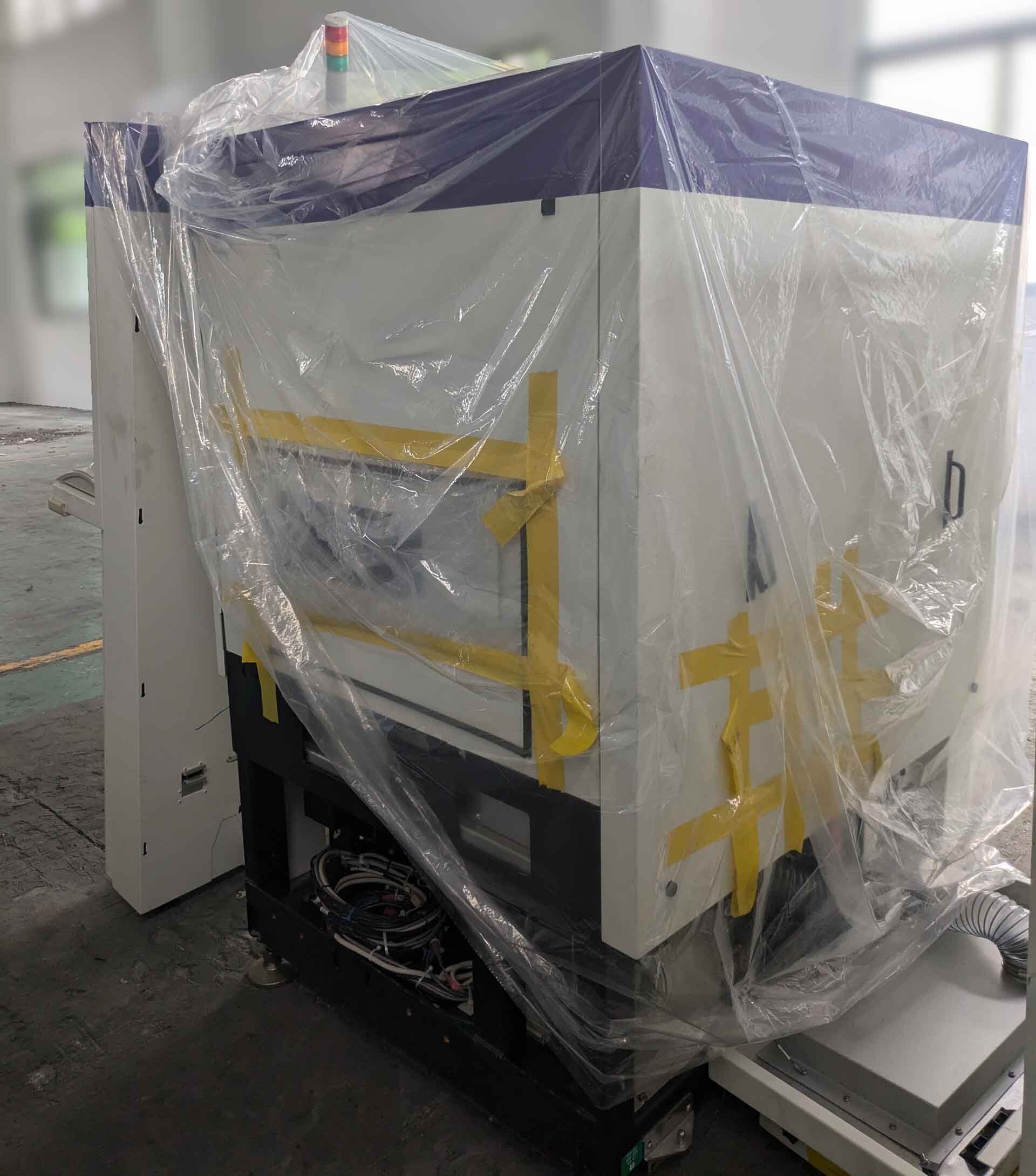
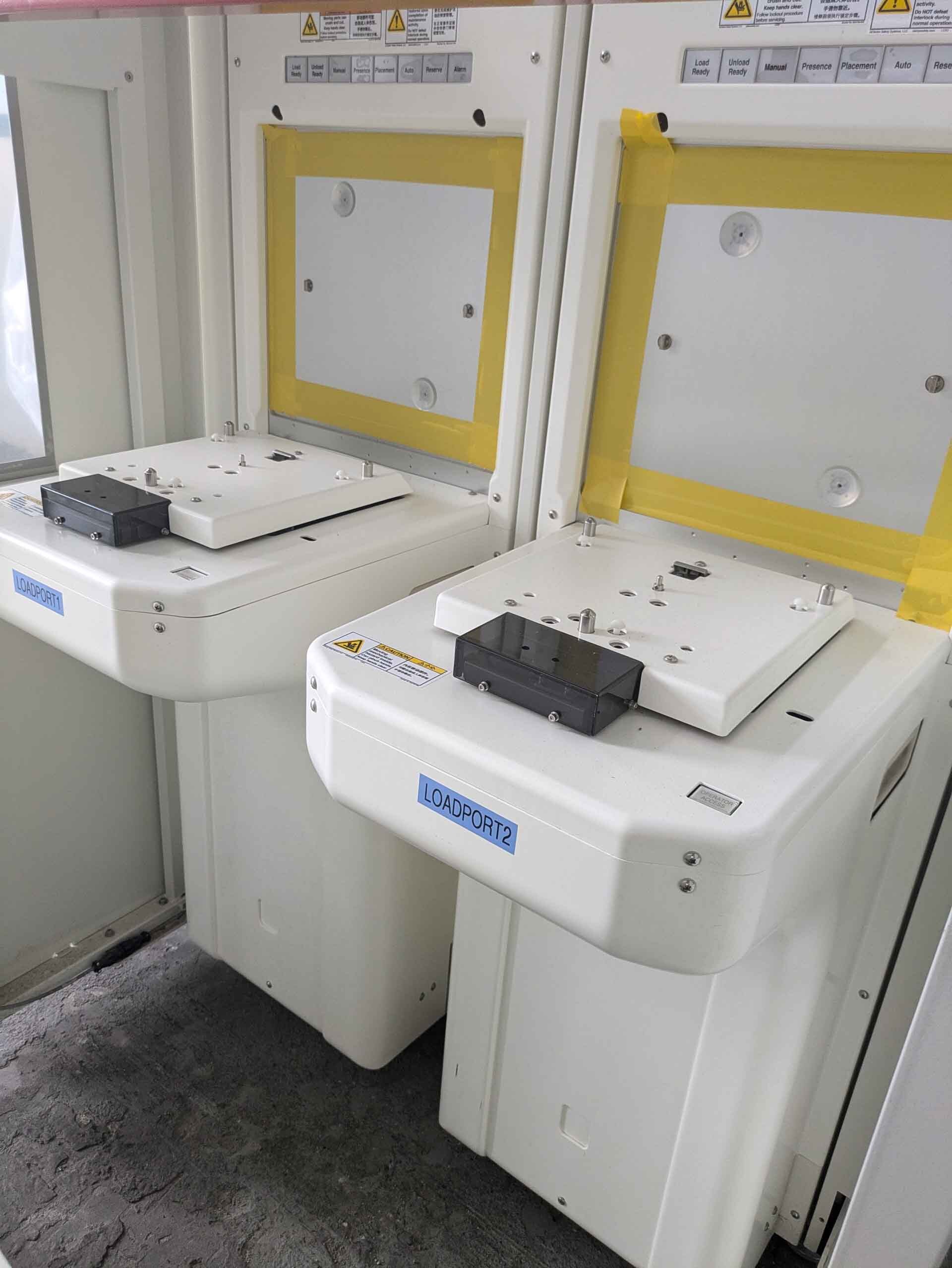
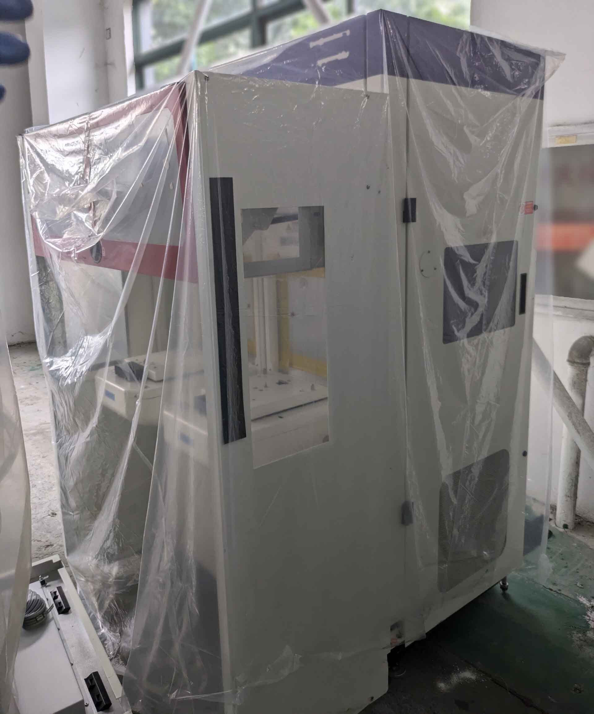
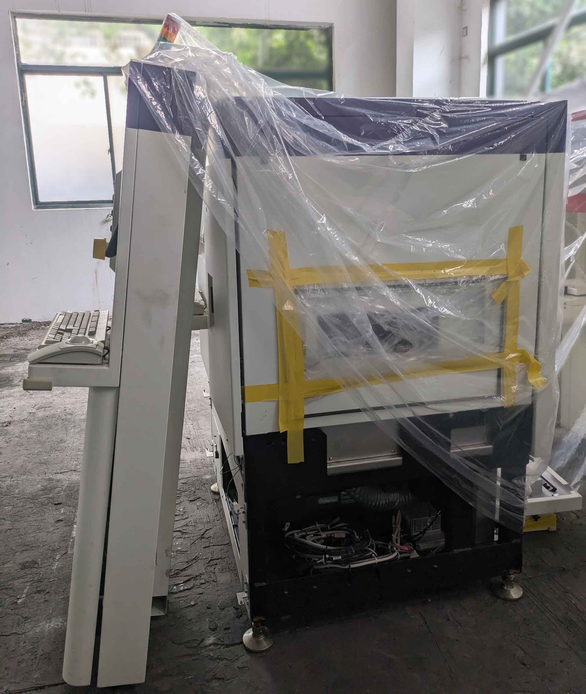
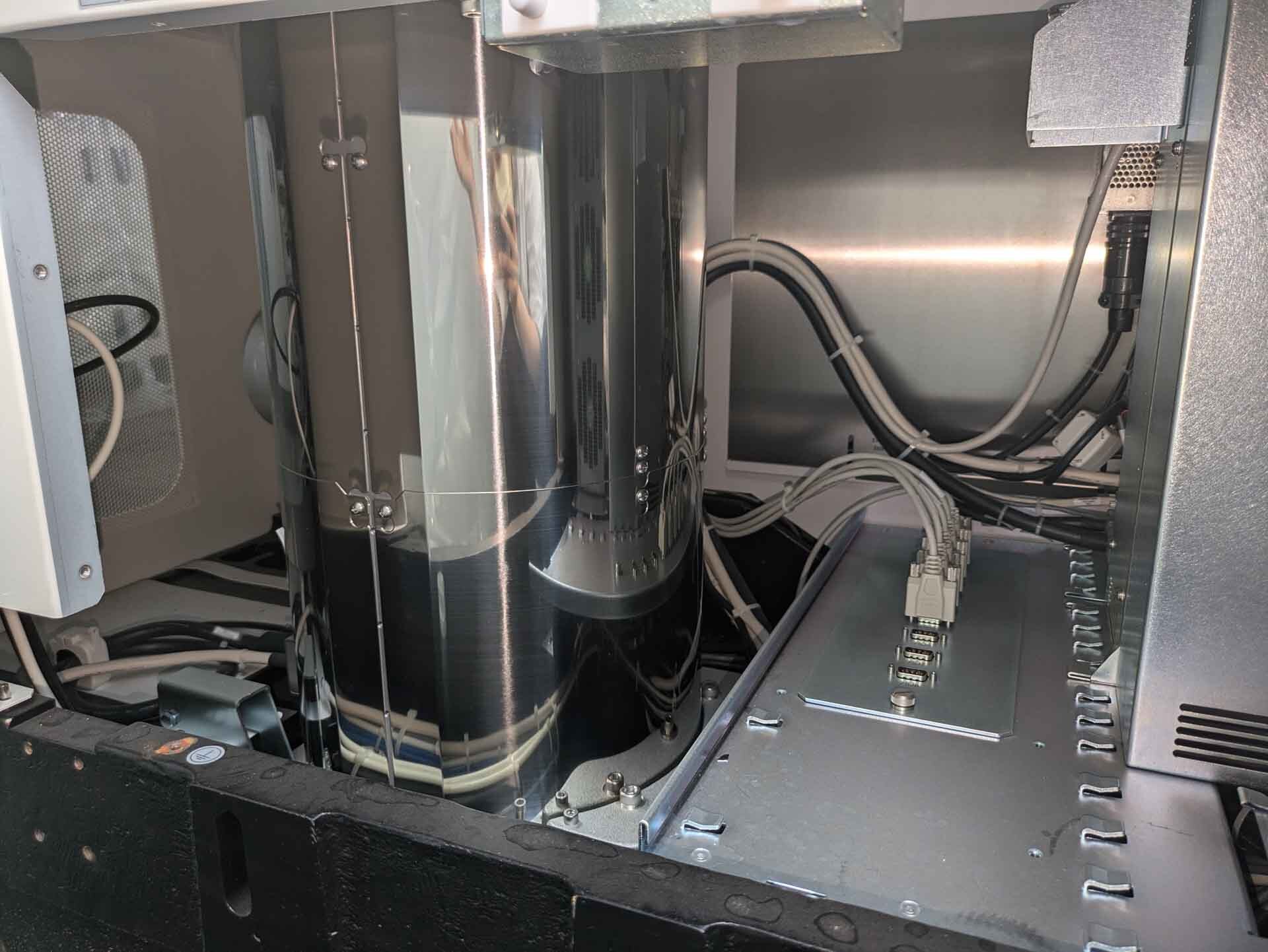
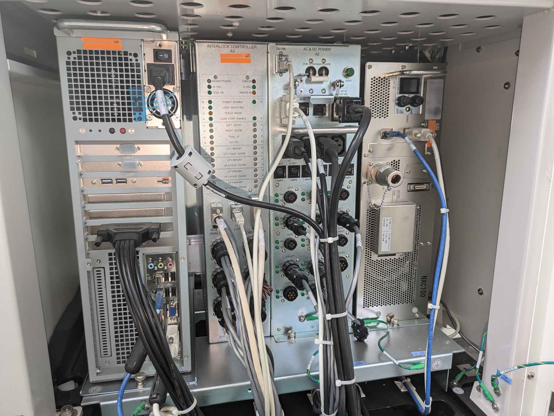
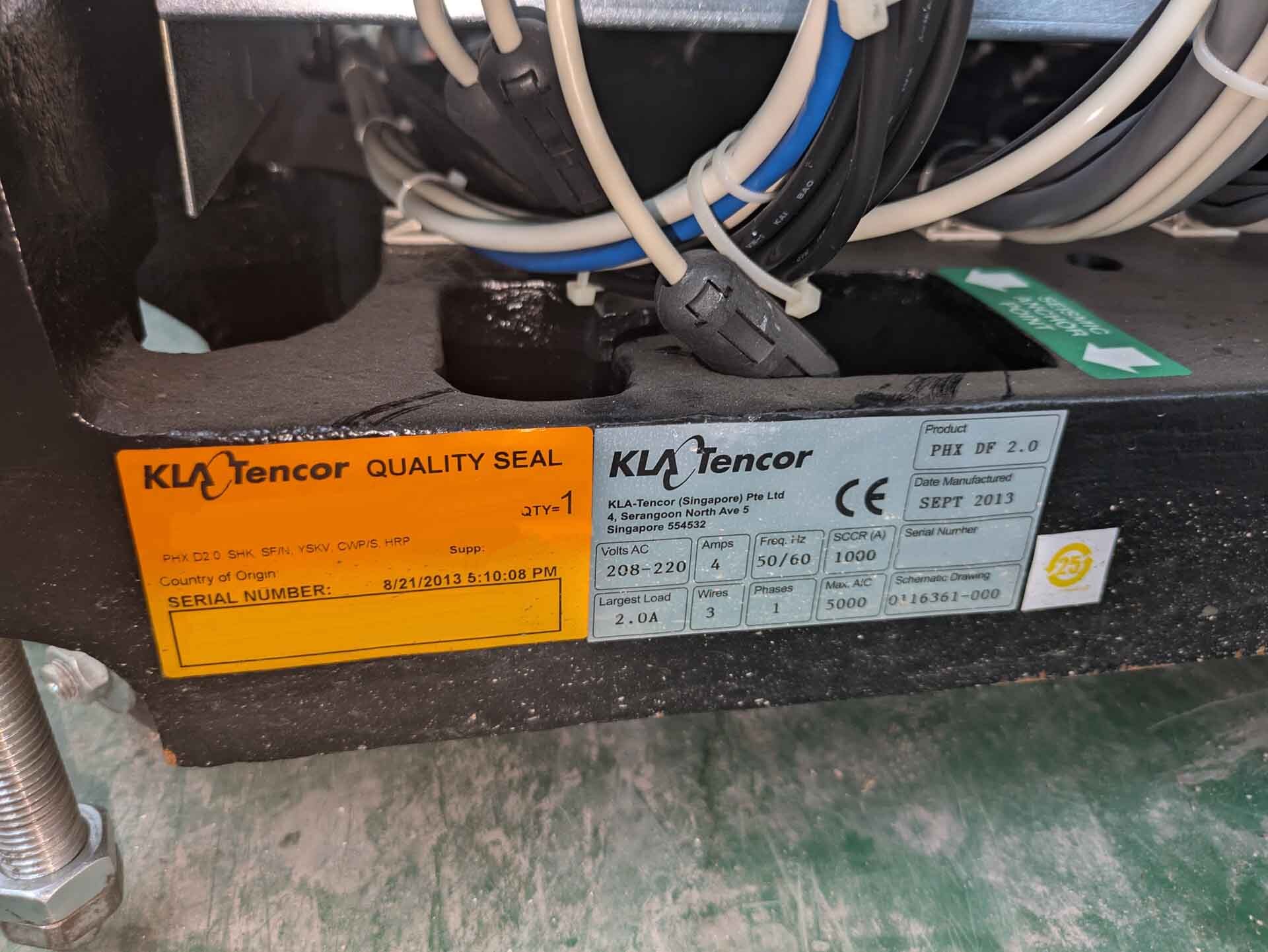
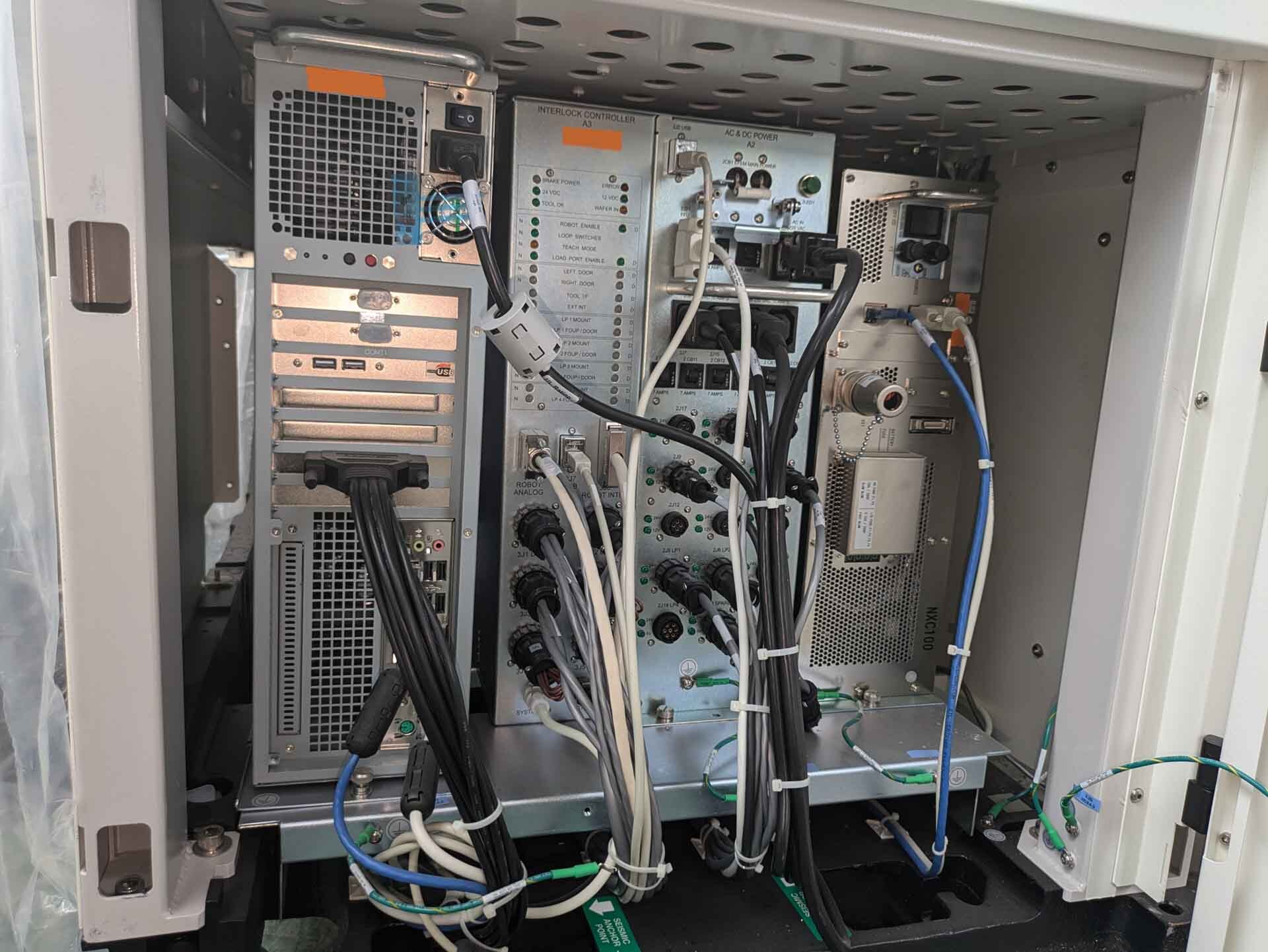
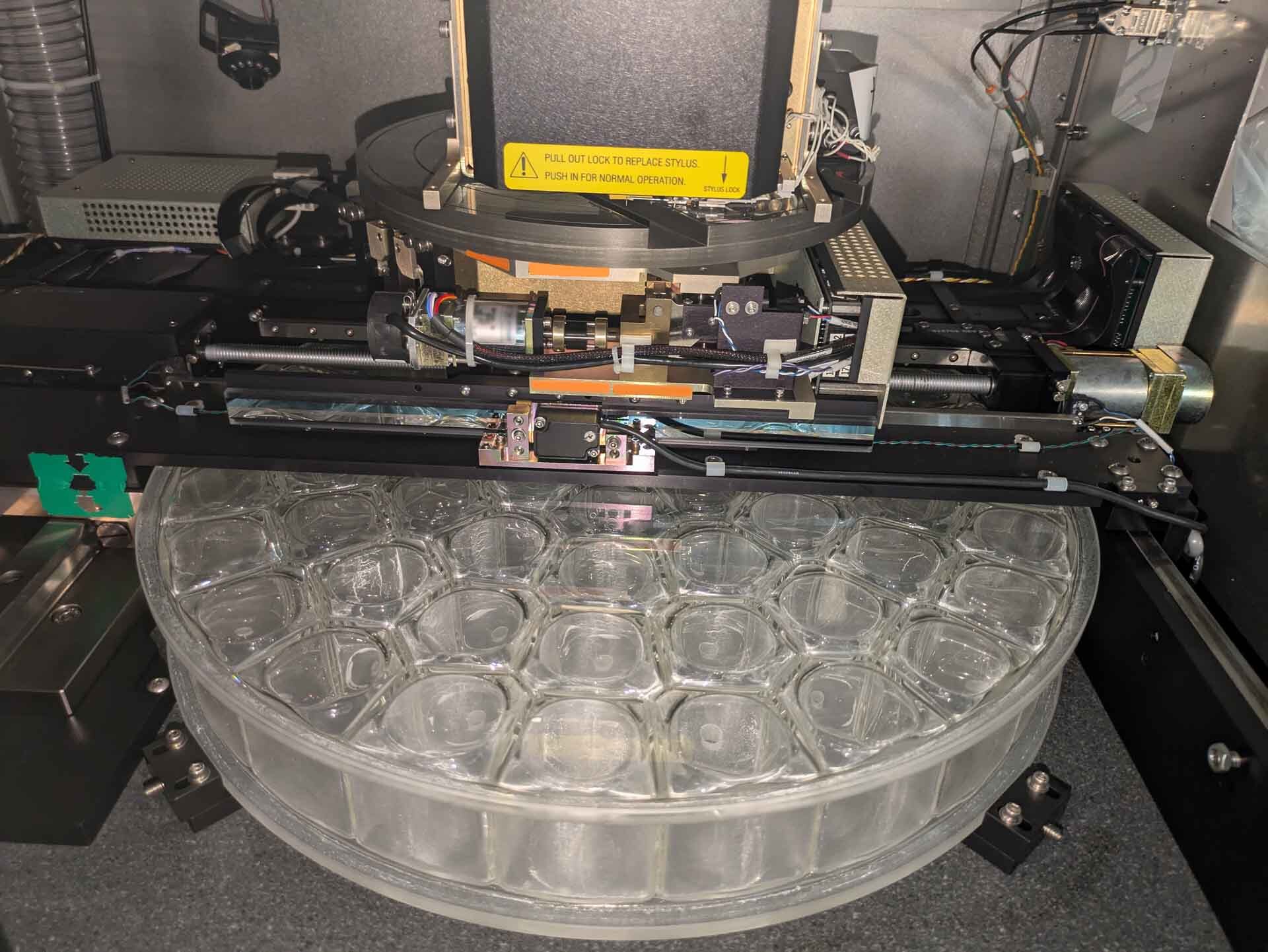
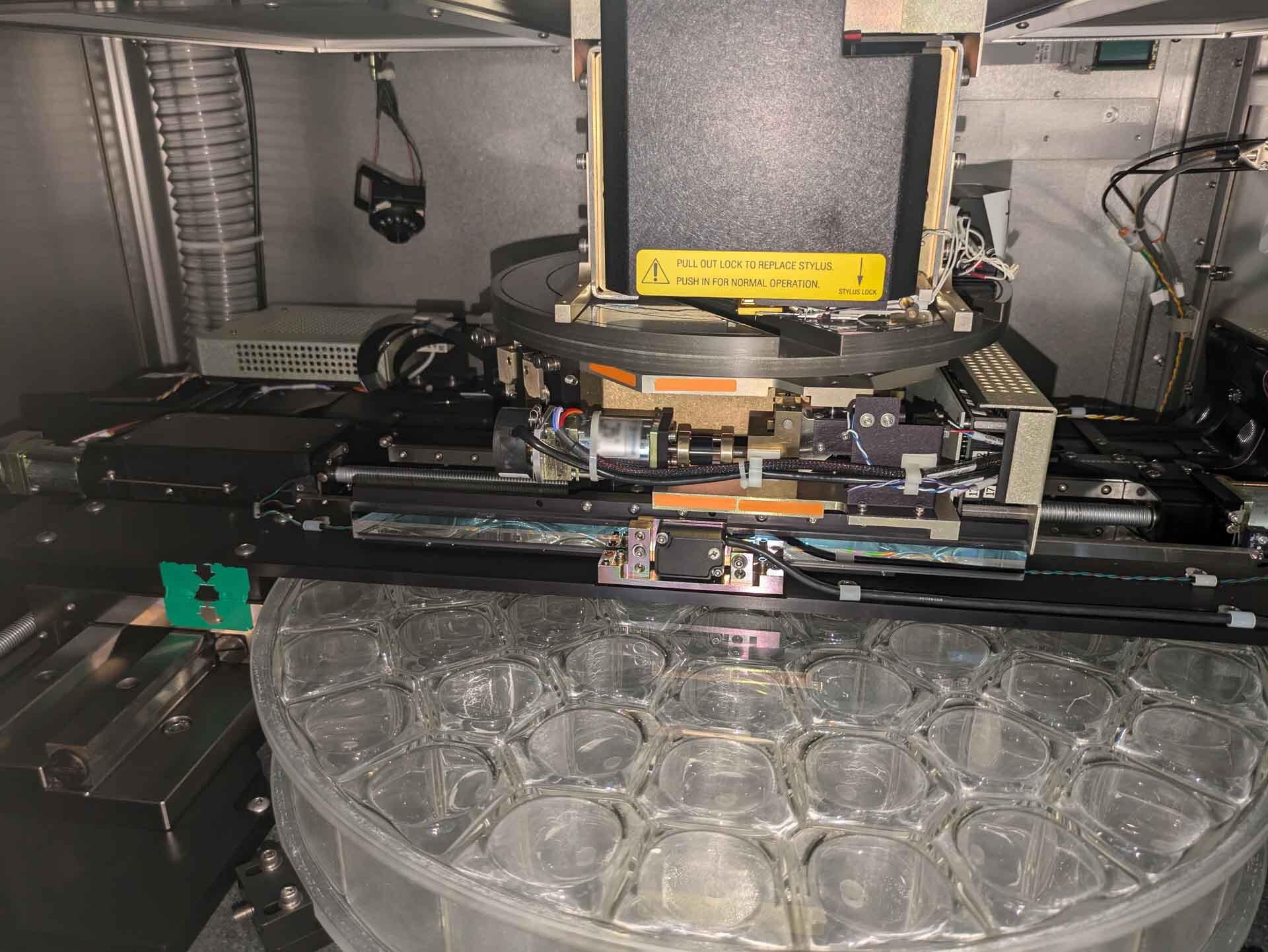
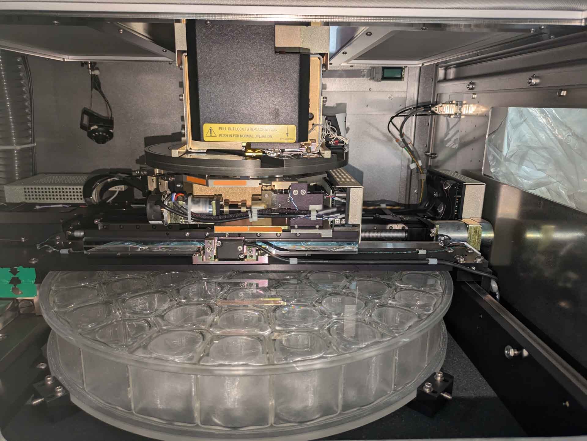
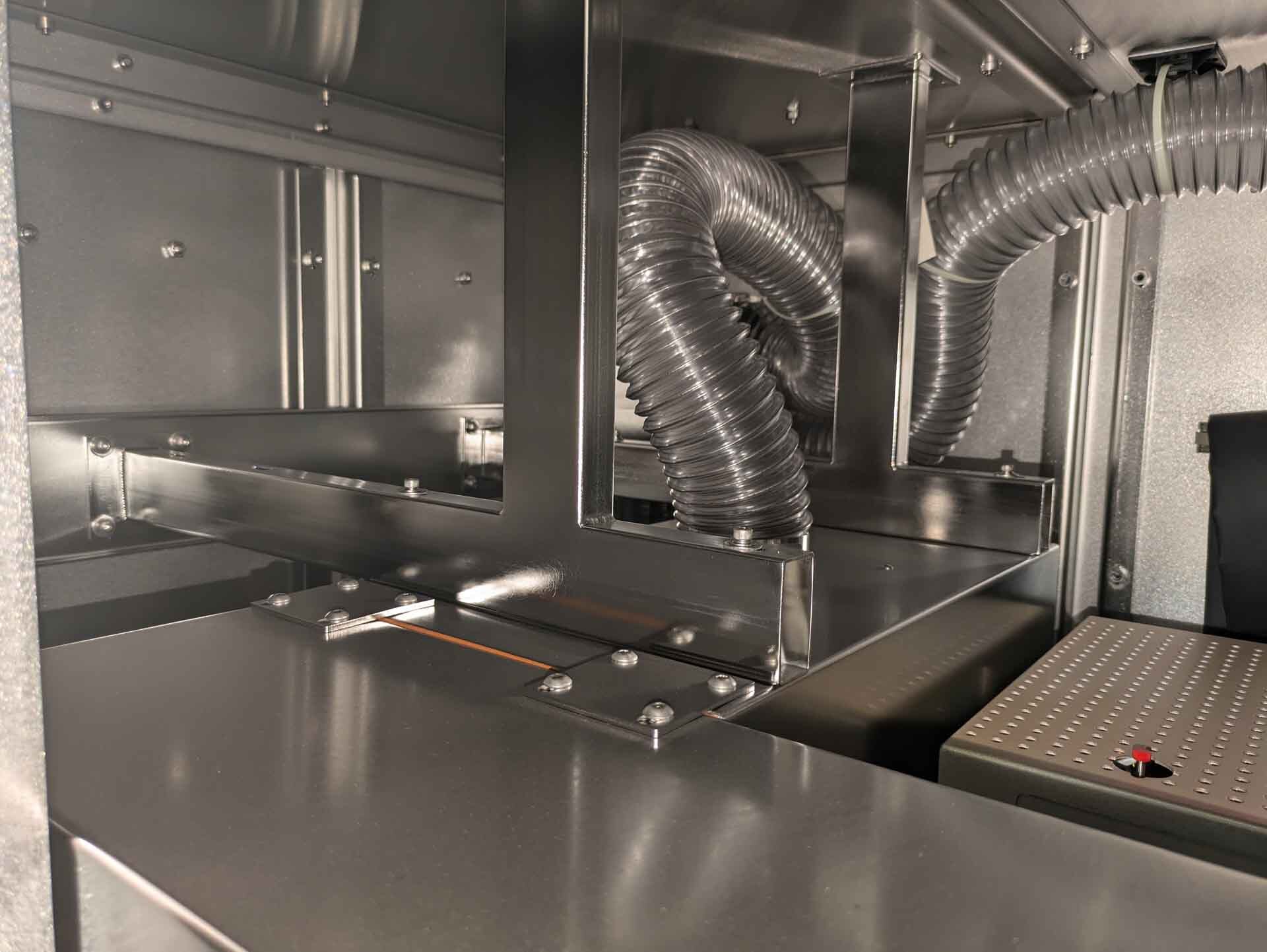
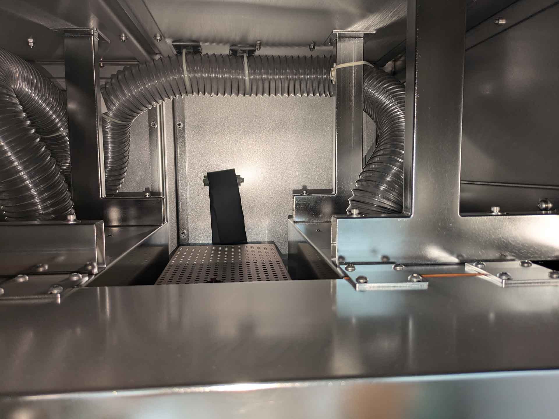
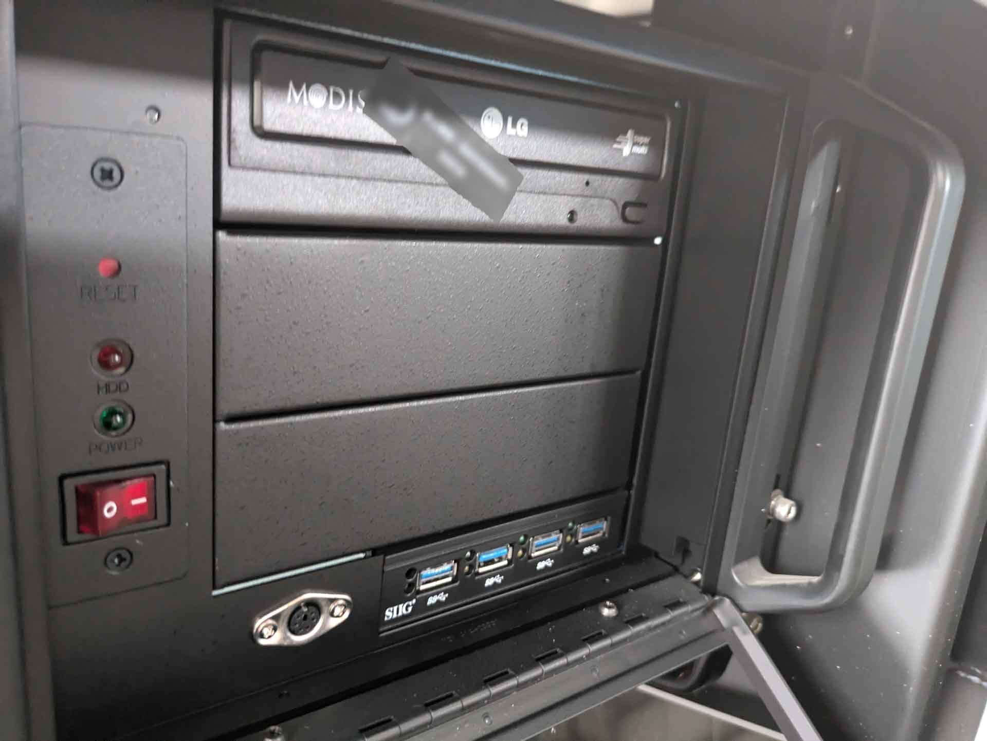
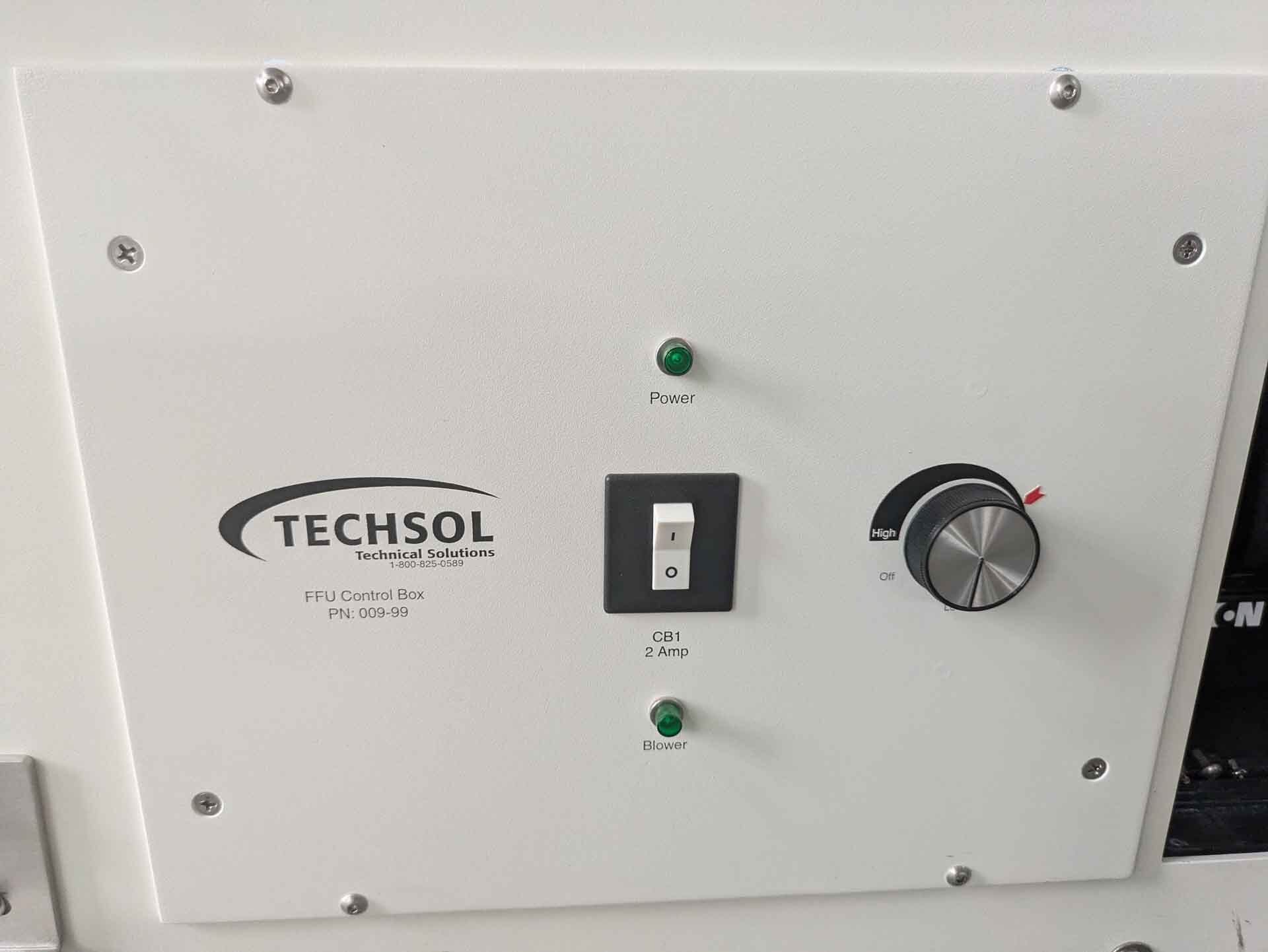
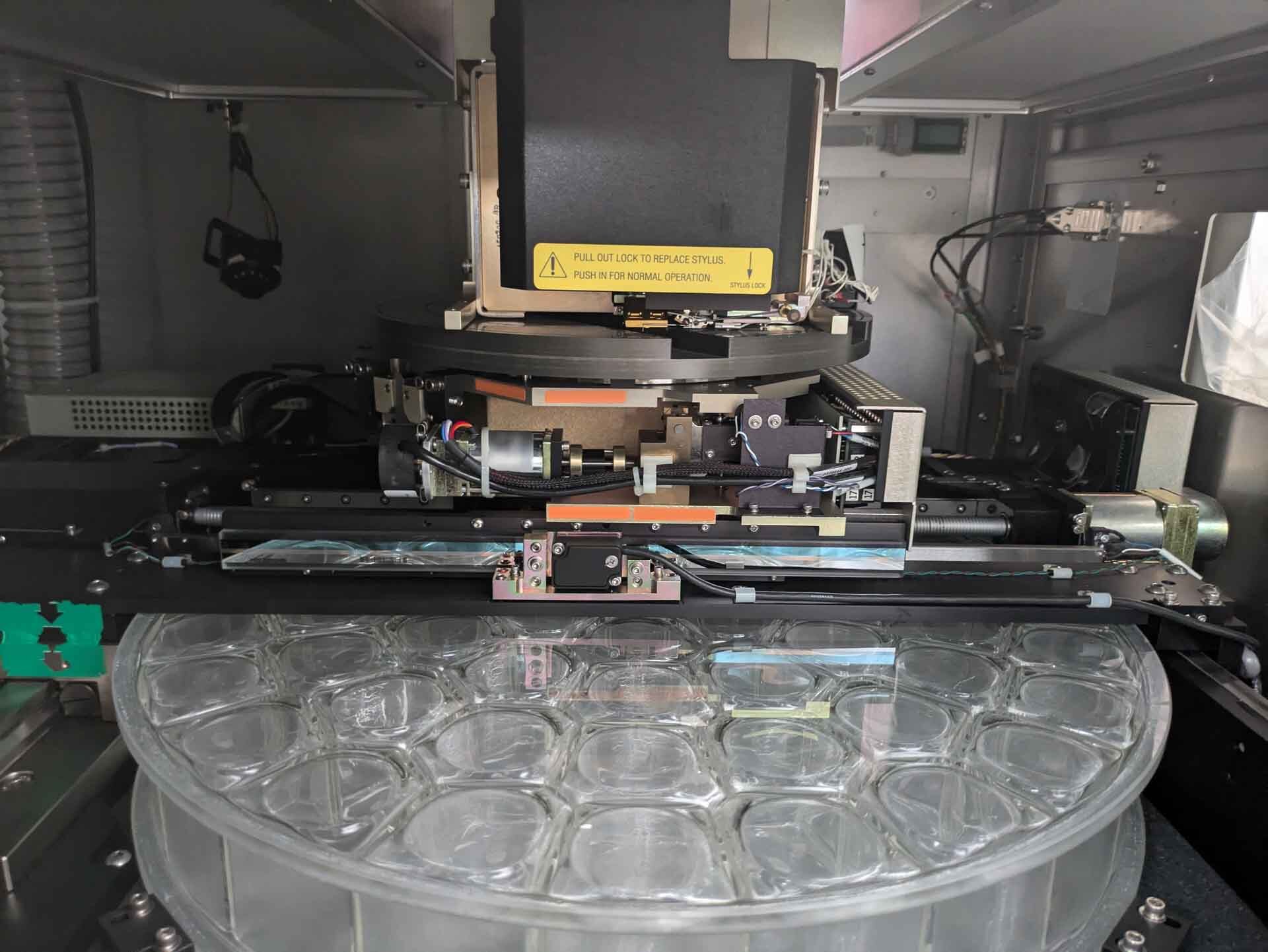
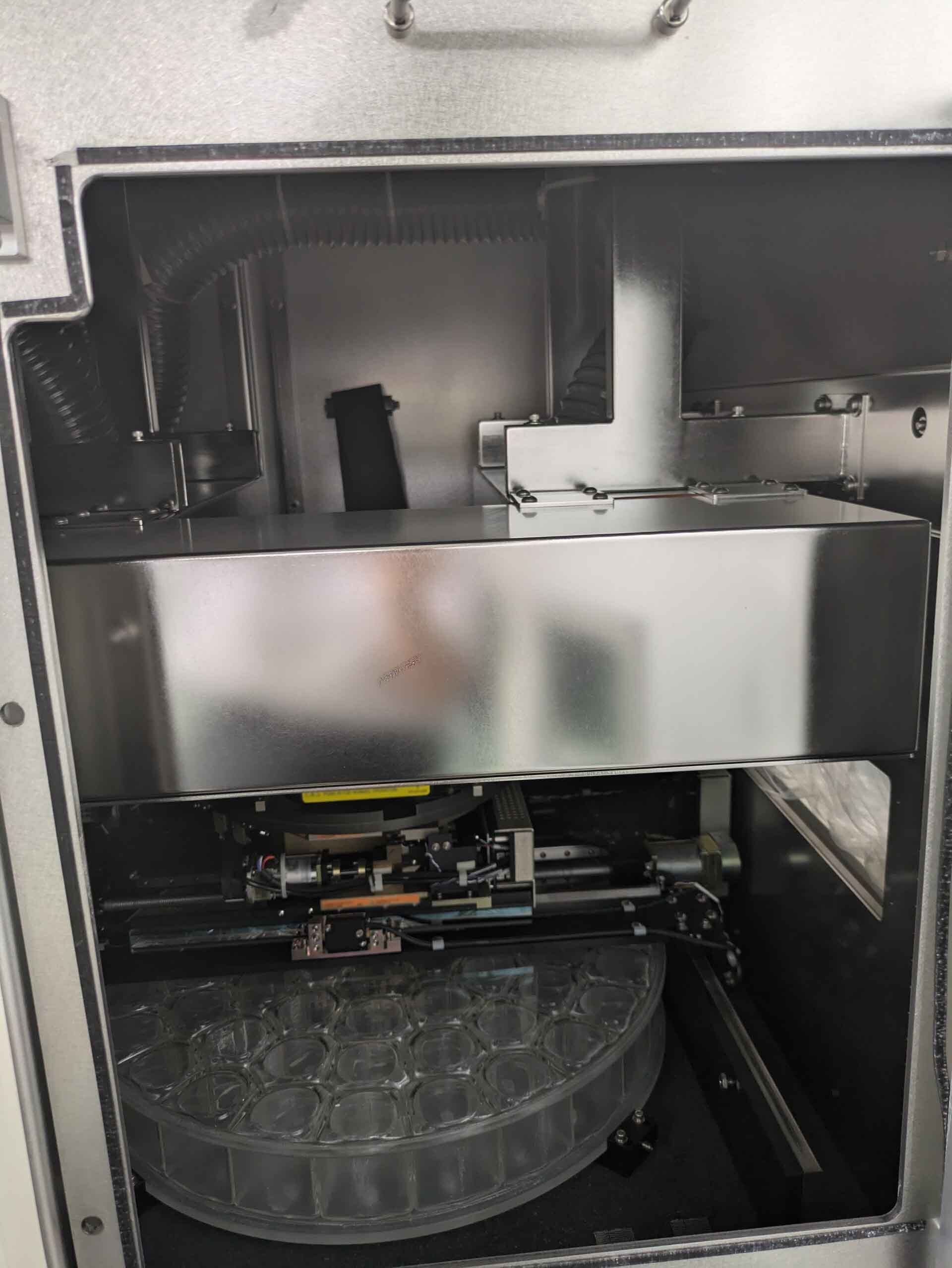
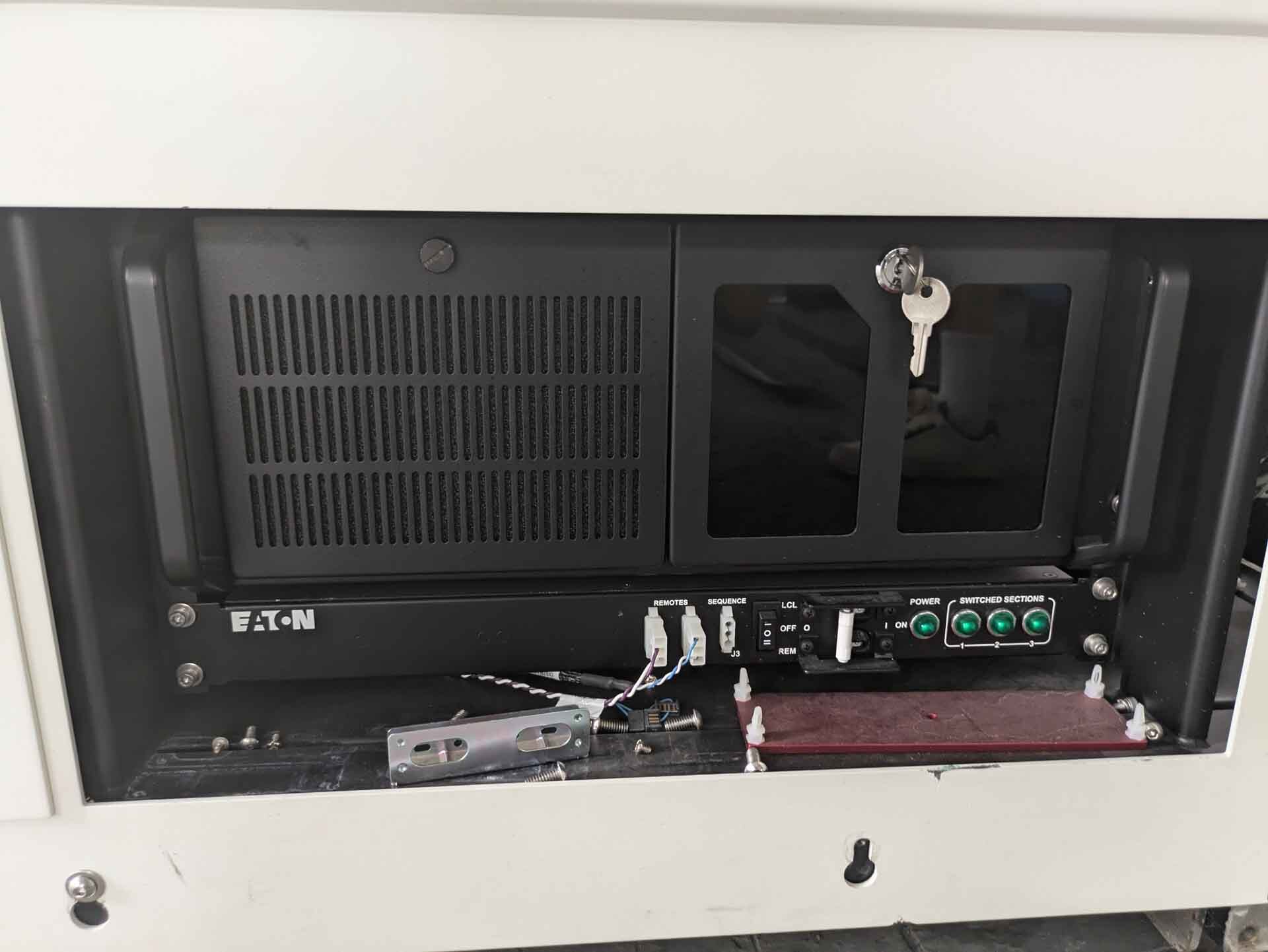
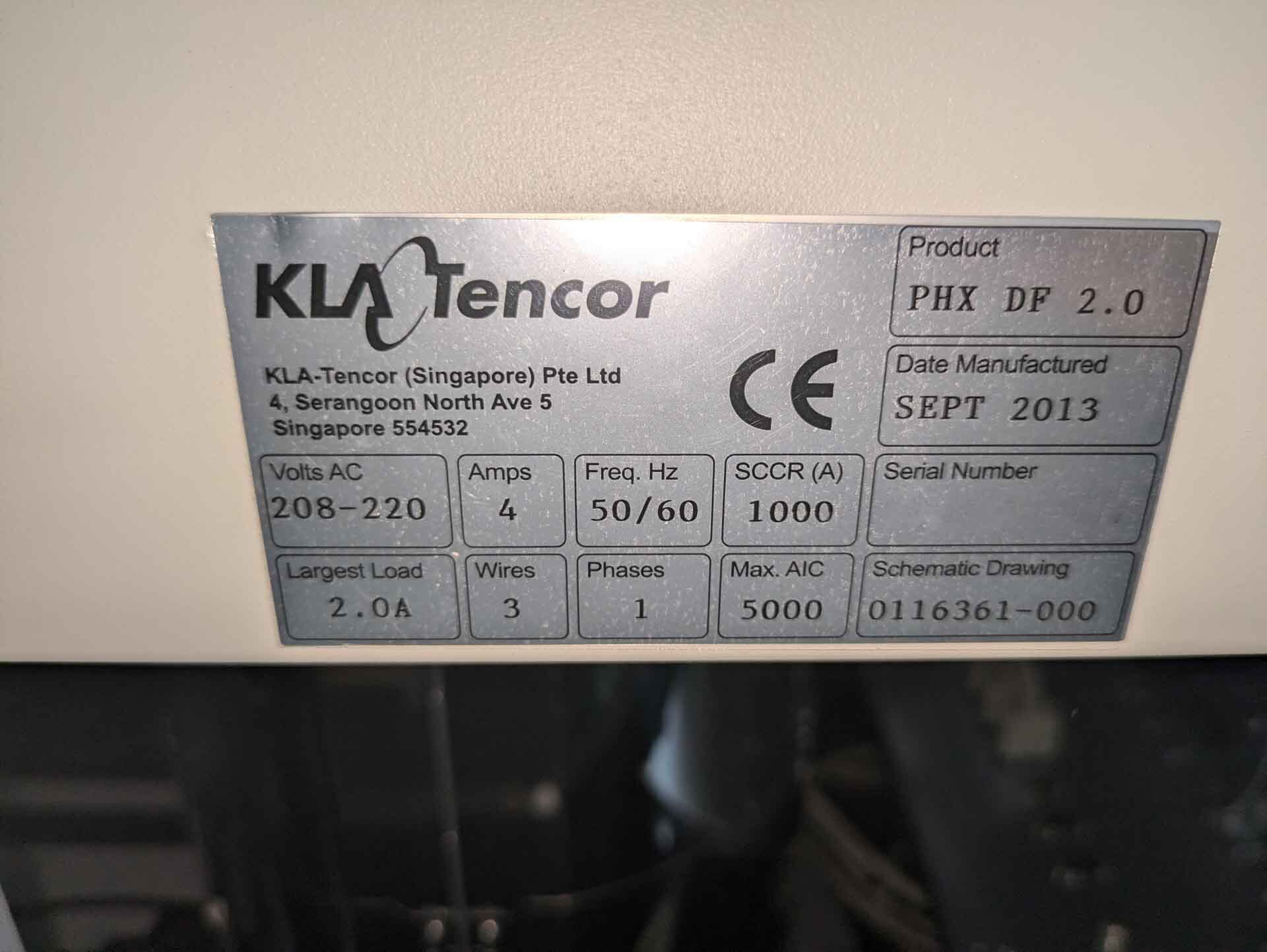
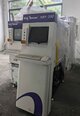
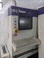
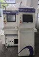
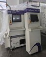
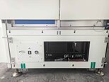
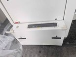
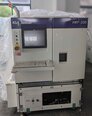
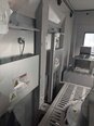
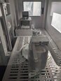
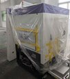
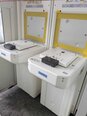
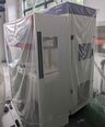
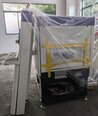
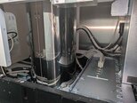
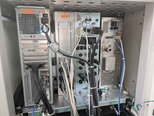
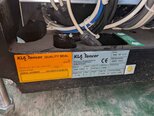
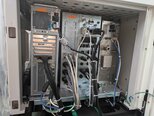
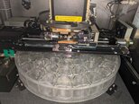
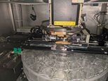
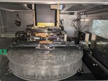
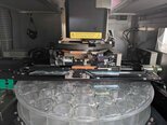
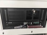
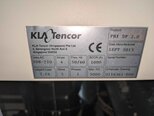
KLA PHX DF 2.0 is a cutting-edge wafer testing and metrology equipment that offers advanced capabilities for semiconductor manufacturers. This system is designed to provide comprehensive solutions for evaluating the quality, performance, and characteristics of wafers used in semiconductor production processes. By integrating various innovative technologies and functionalities, the PHX DF 2.0 delivers precise and accurate measurements to ensure high yield and reliability in semiconductor manufacturing. One of the key features of TENCOR PHX DF 2.0 unit is its ability to perform defect detection and classification on wafers with exceptional sensitivity and speed. Utilizing sophisticated imaging techniques and advanced algorithms, this machine can identify and analyze various types of defects present on the wafer surface, such as particles, scratches, and patterns, at a microscopic level. By detecting these defects early in the manufacturing process, semiconductor manufacturers can take corrective actions to minimize yield losses and improve overall wafer quality. Moreover, the PHX DF 2.0 tool offers advanced metrology capabilities for measuring critical parameters of semiconductor wafers with high precision and accuracy. Through the integration of advanced optical and laser-based measurement technologies, this asset can analyze various characteristics of wafers, including thickness, roughness, flatness, and pattern uniformity. These measurements are essential for controlling process variability and ensuring consistent performance of semiconductor devices. In addition to defect detection and metrology, KLA / TENCOR PHX DF 2.0 model provides automated wafer handling and inspection functionalities to streamline the manufacturing process. The equipment is equipped with robotic arms, wafer mapping tools, and software modules that enable seamless loading, positioning, and scanning of wafers for comprehensive analysis. This automation capability not only enhances productivity and throughput but also reduces manual errors and operator intervention, leading to greater efficiency in semiconductor manufacturing. Furthermore, the PHX DF 2.0 system features a user-friendly interface and intuitive software platform that allows semiconductor manufacturers to easily configure, control, and monitor the testing and metrology processes. The unit offers real-time visualization tools, data analysis capabilities, and reporting functionalities to help users make informed decisions and optimize production processes. Additionally, the machine can be integrated with other equipment and factory systems through industry-standard communication protocols, enabling data sharing and synchronization for improved operational efficiency. Overall, KLA PHX DF 2.0 wafer testing and metrology tool is a sophisticated solution that leverages advanced technologies to enable semiconductor manufacturers to achieve higher yields, improve product quality, and enhance process control in semiconductor manufacturing. With its comprehensive defect detection, metrology, automation, and data management features, this asset sets a new standard for wafer inspection and analysis in the semiconductor industry, paving the way for faster innovation and higher performance in semiconductor devices.
There are no reviews yet