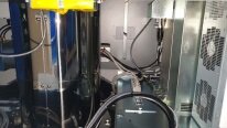
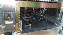
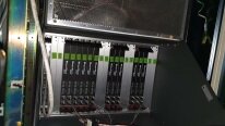
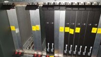
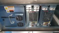
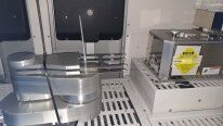
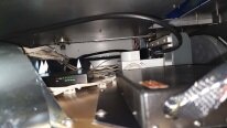
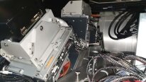
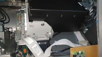
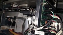
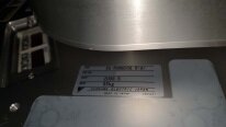
Used KLA / TENCOR Puma 9000 #9240145 for sale
URL successfully copied!
Tap to zoom


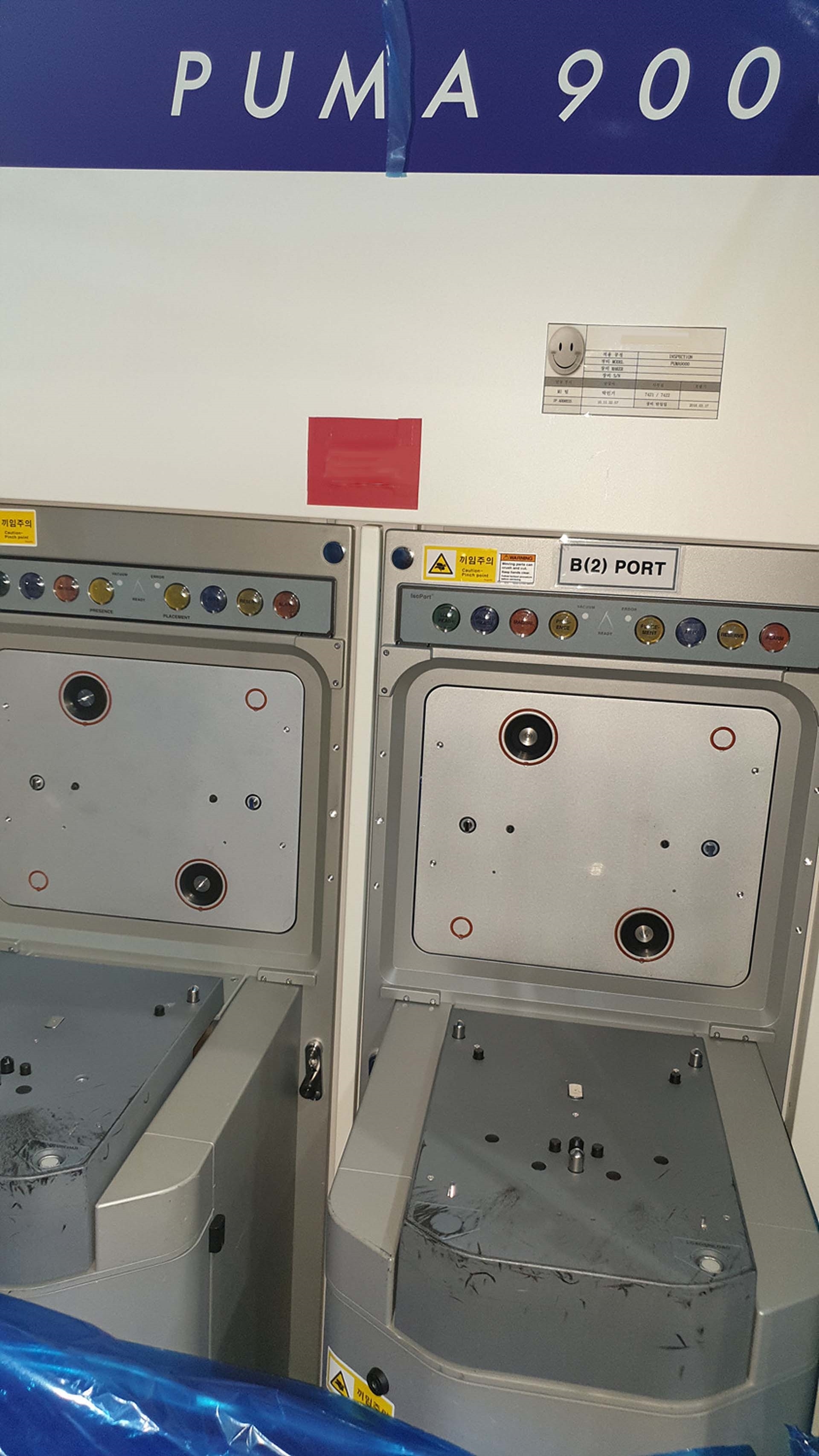











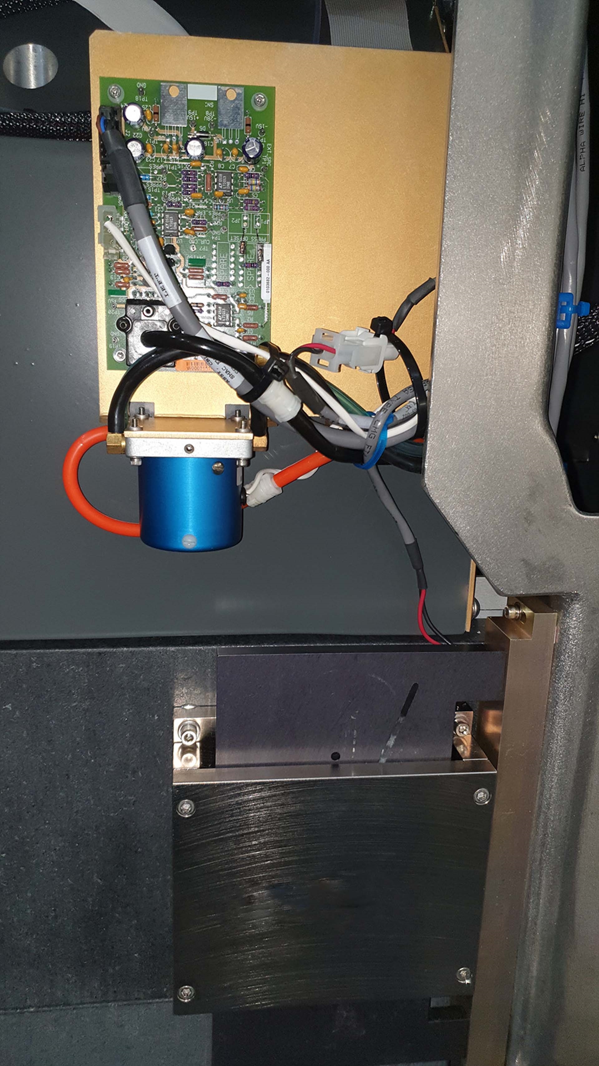

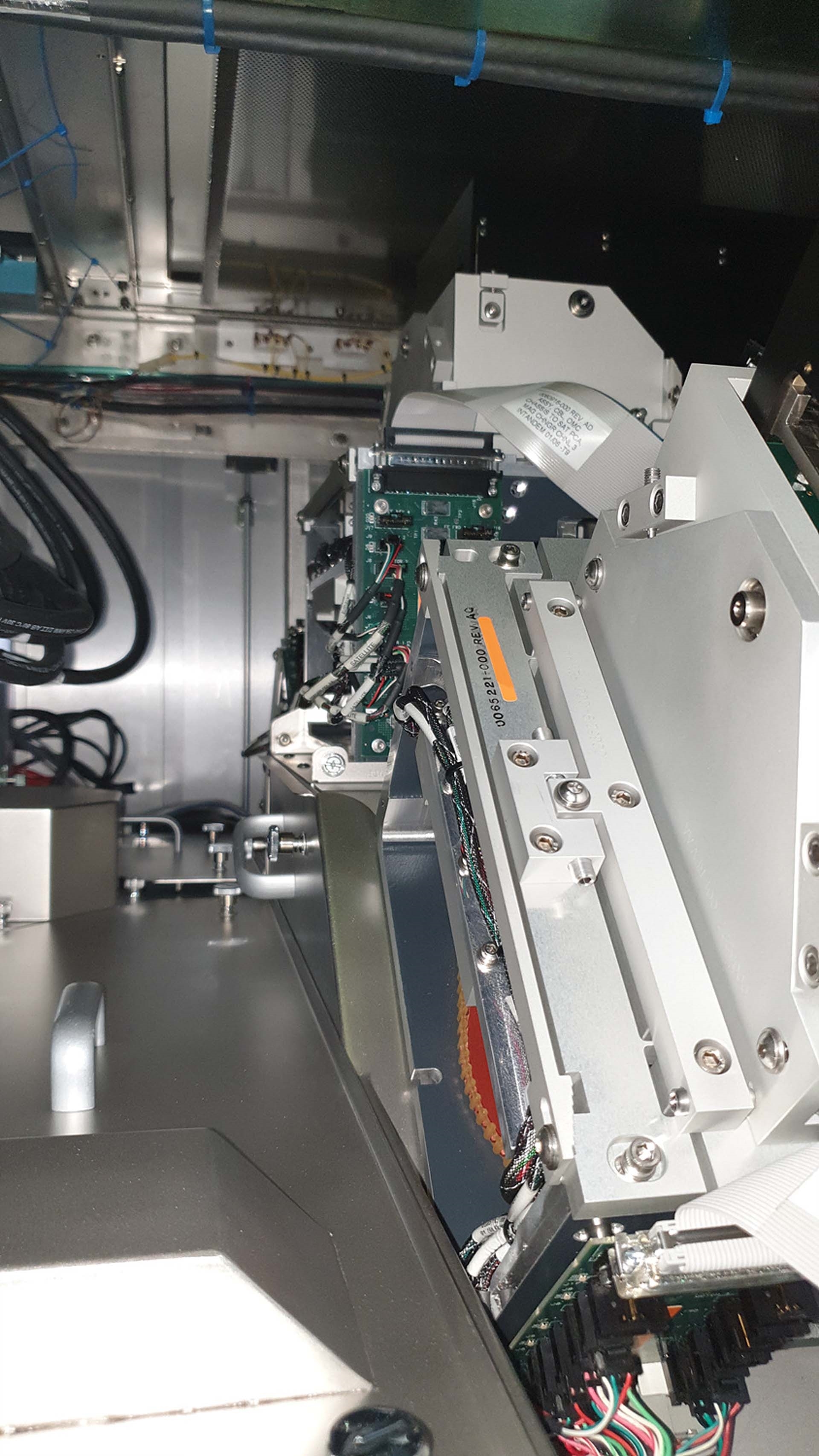


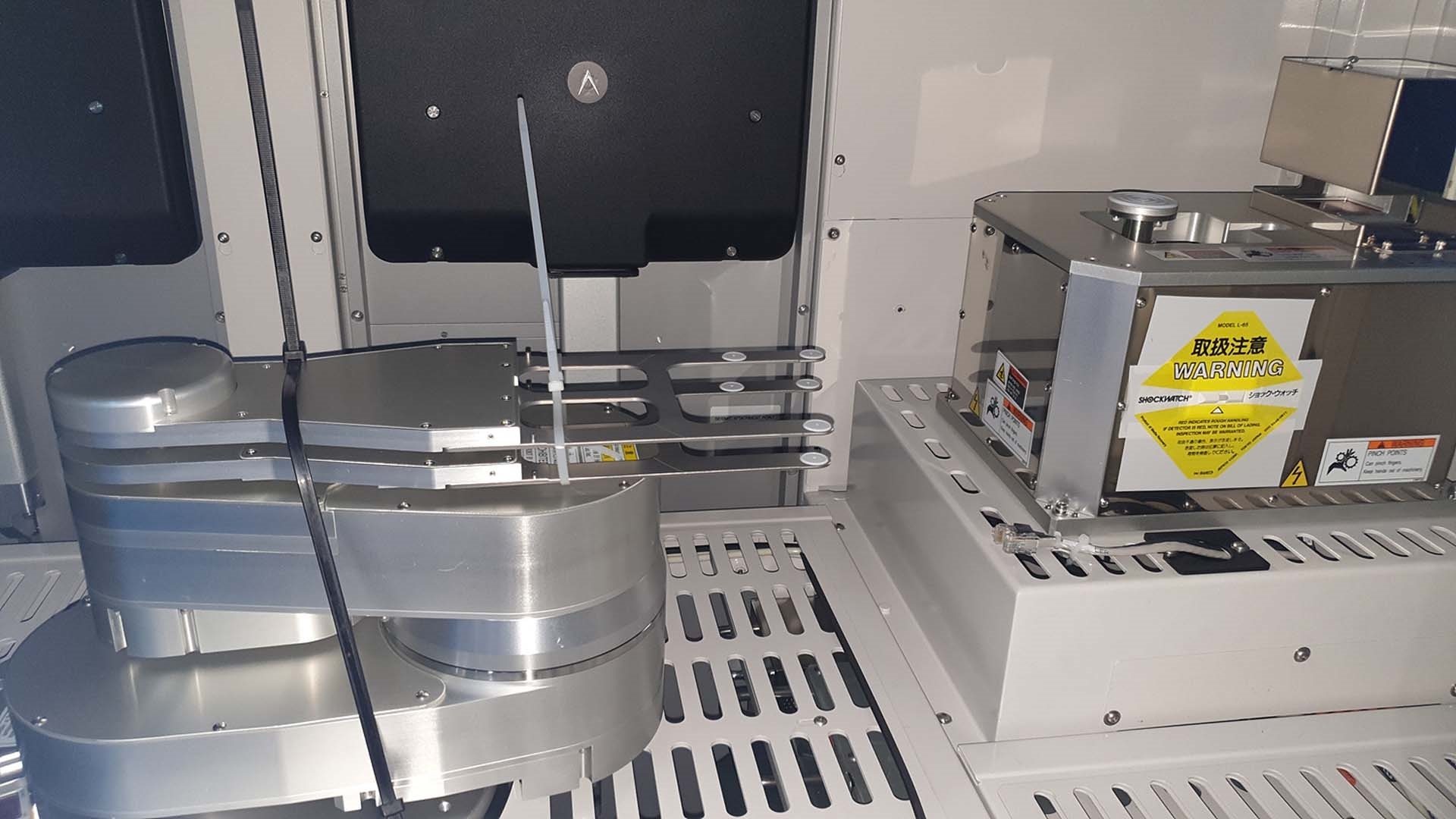

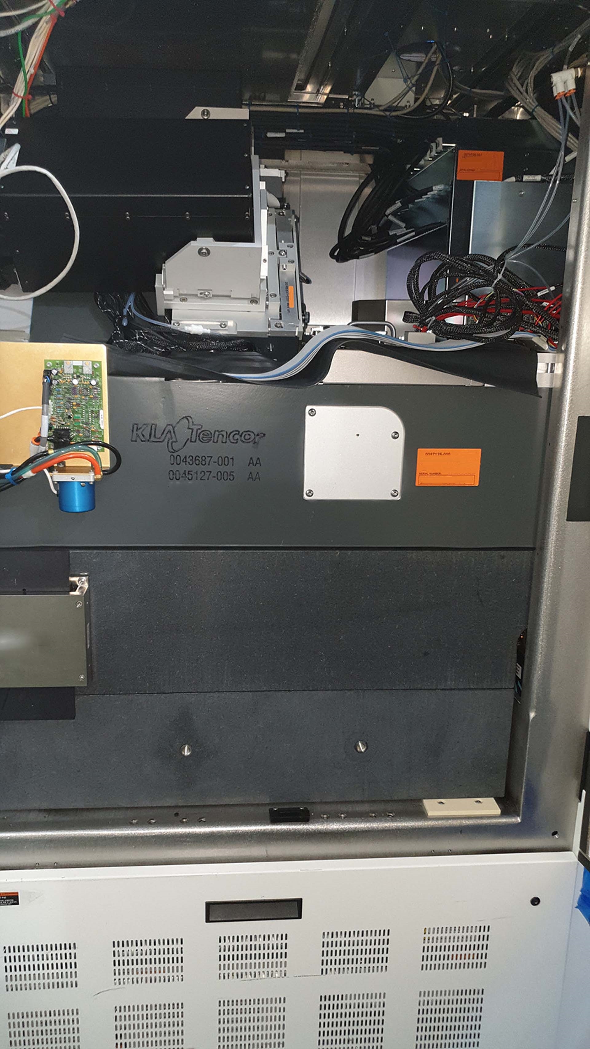








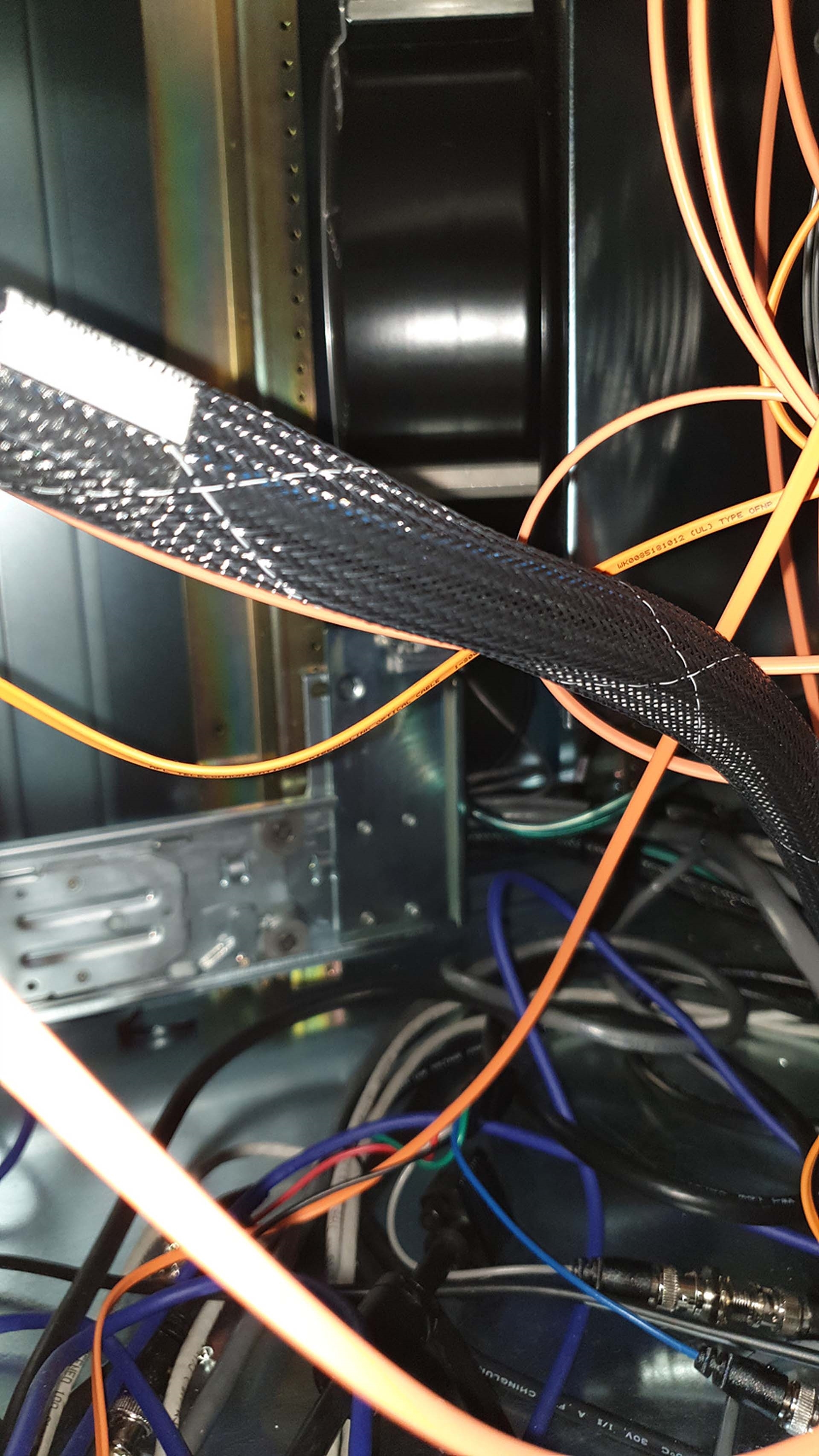

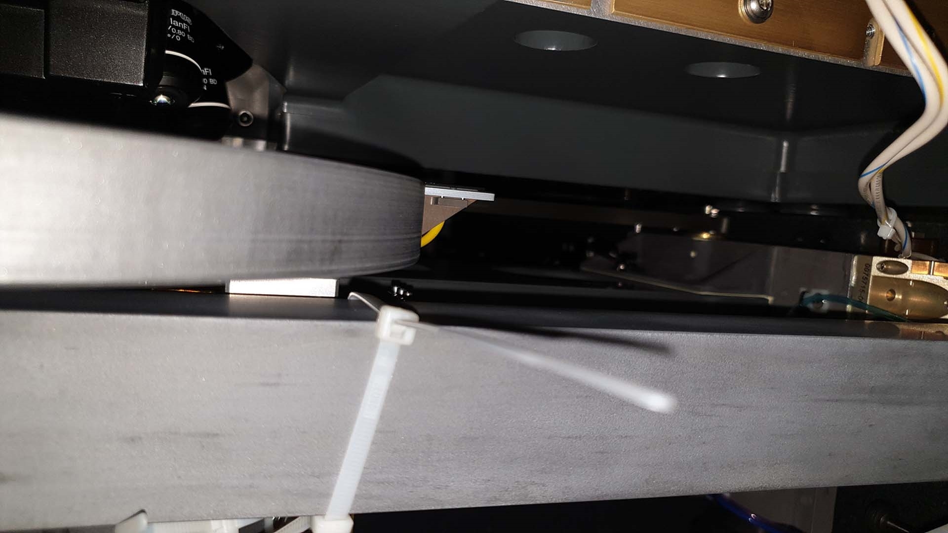

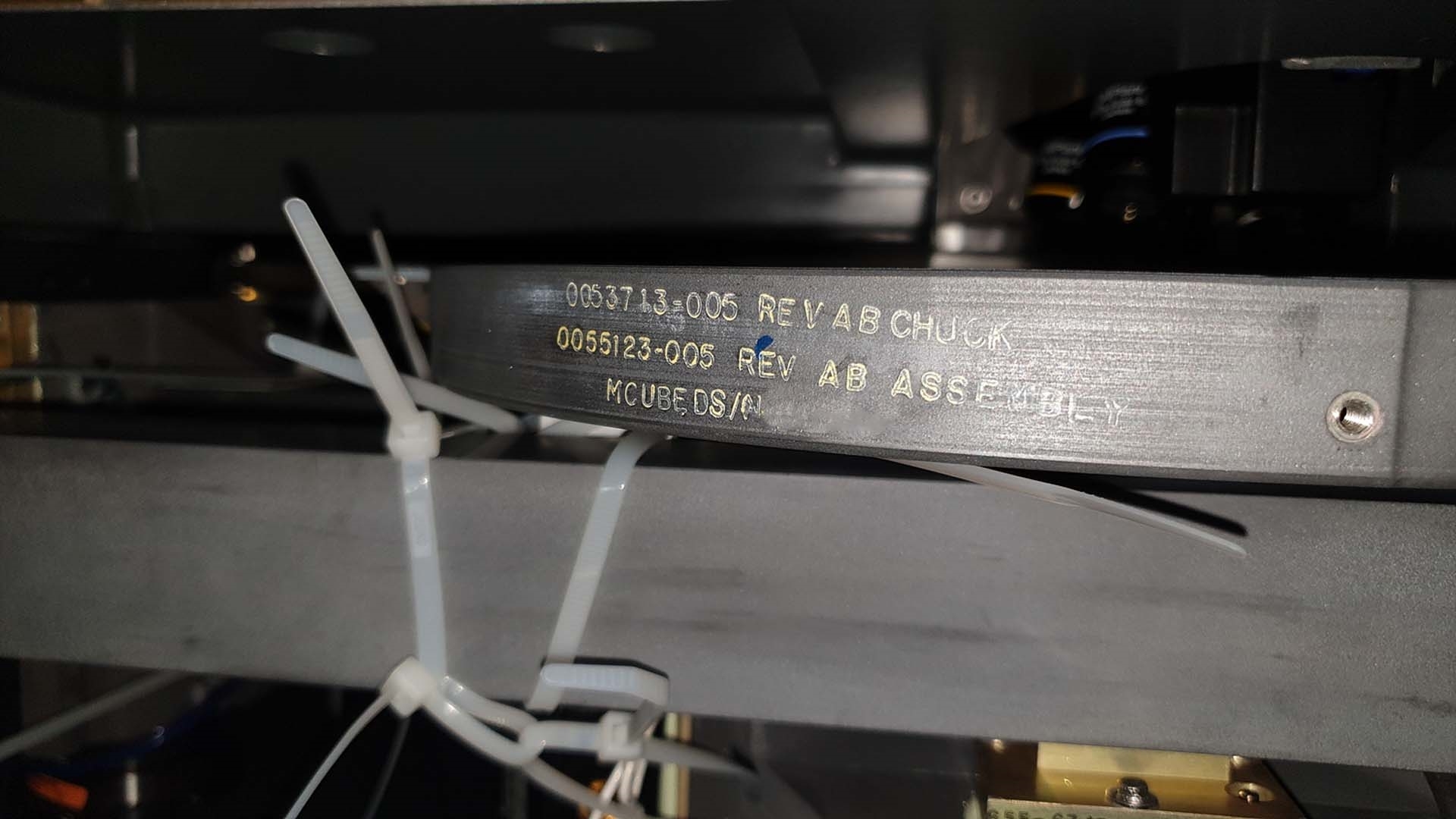

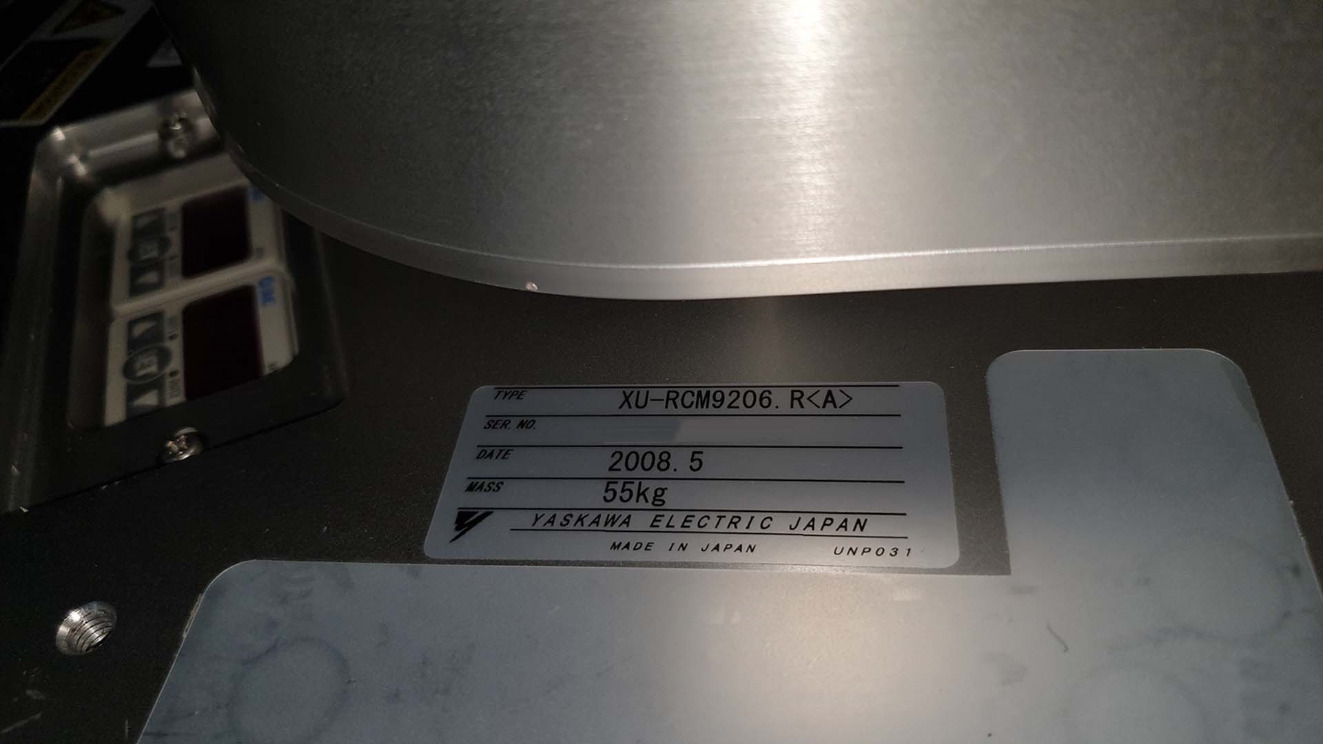

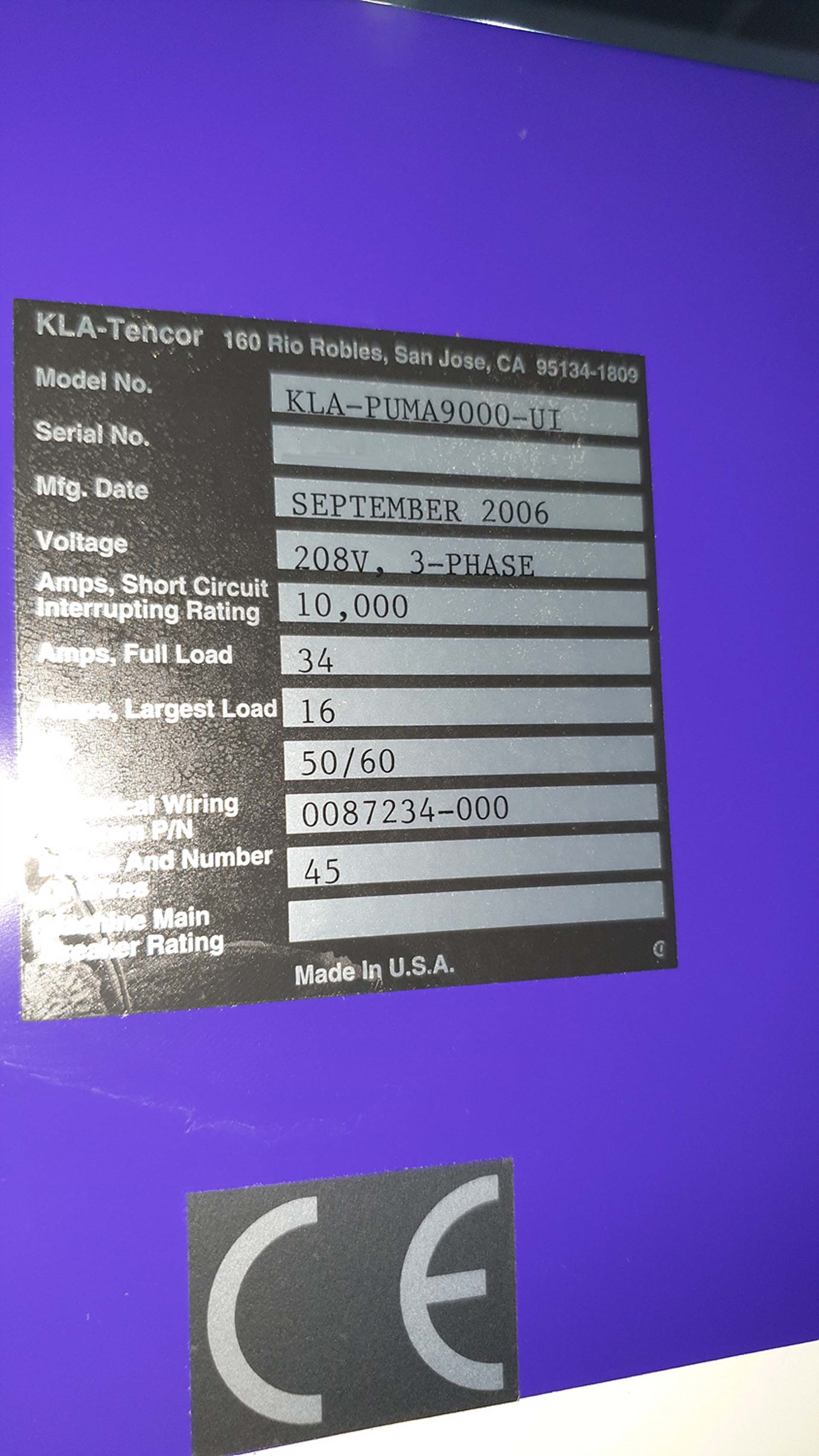

ID: 9240145
Vintage: 2006
Darkfield inspection system
Module: User interface
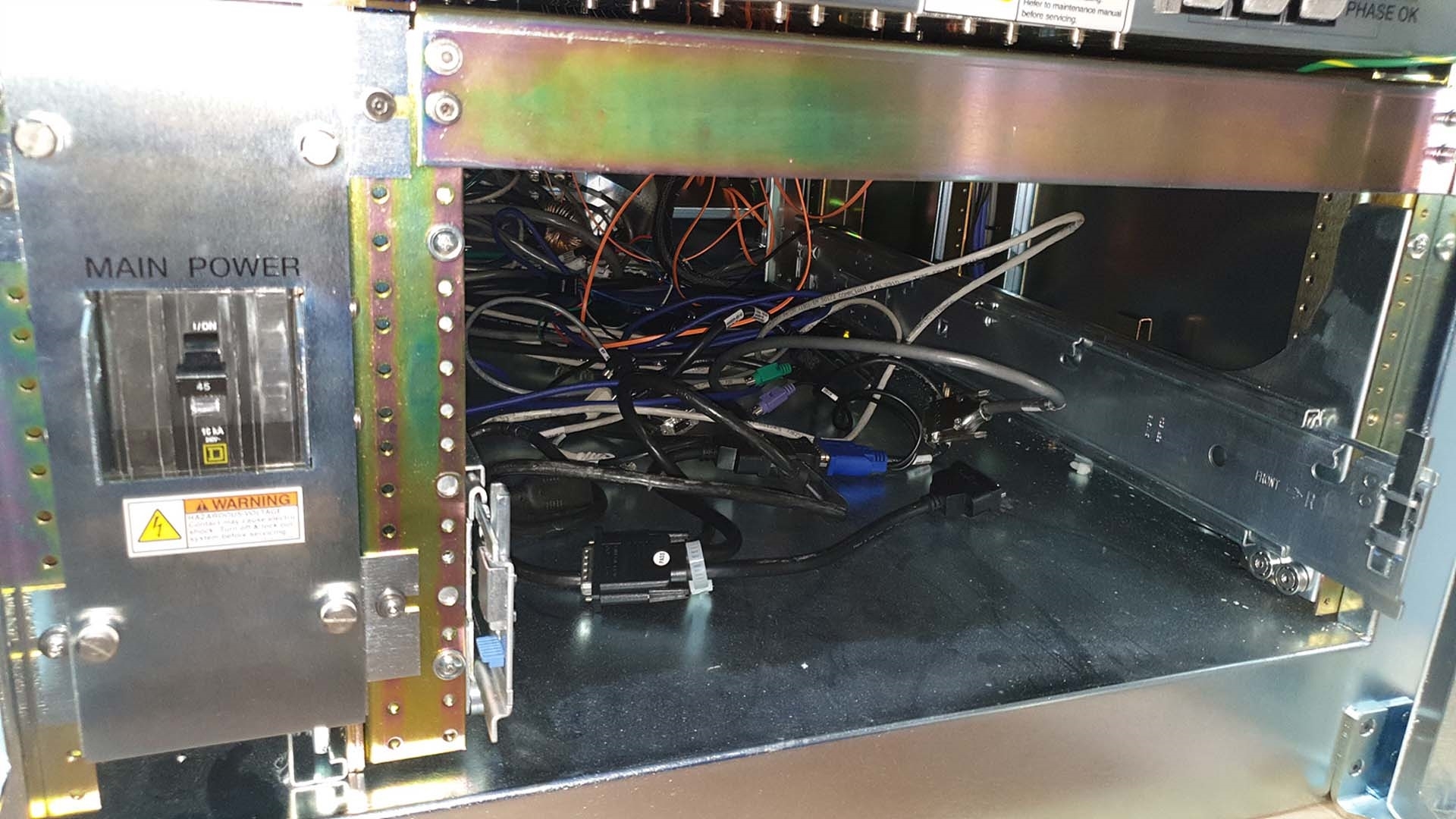
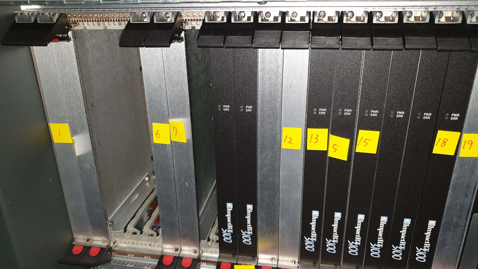
Missing parts:
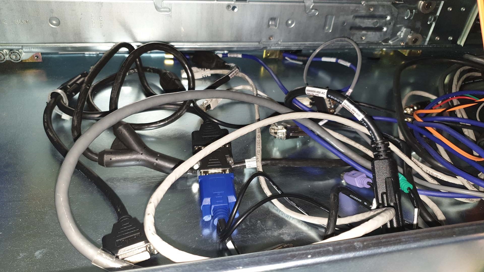
PC
(2) Boards
2006 vintage.
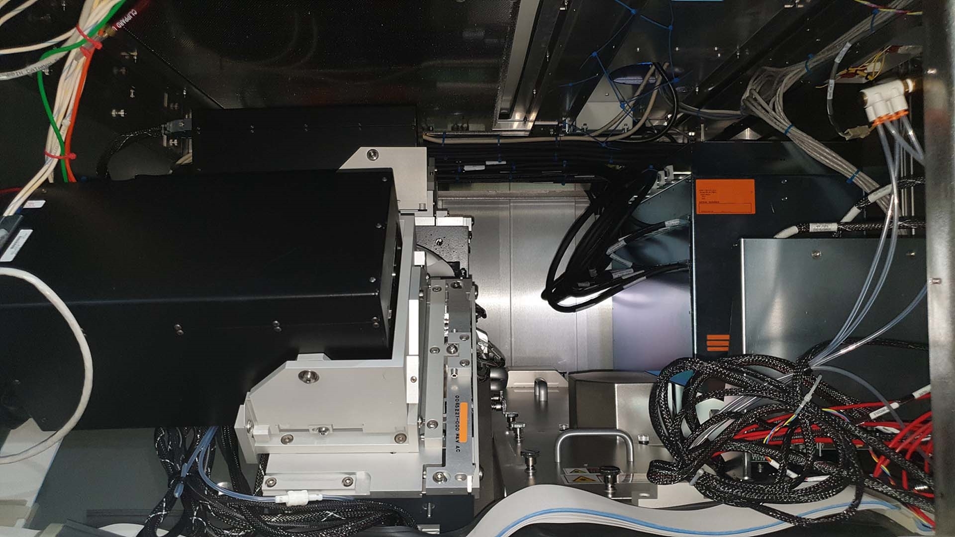
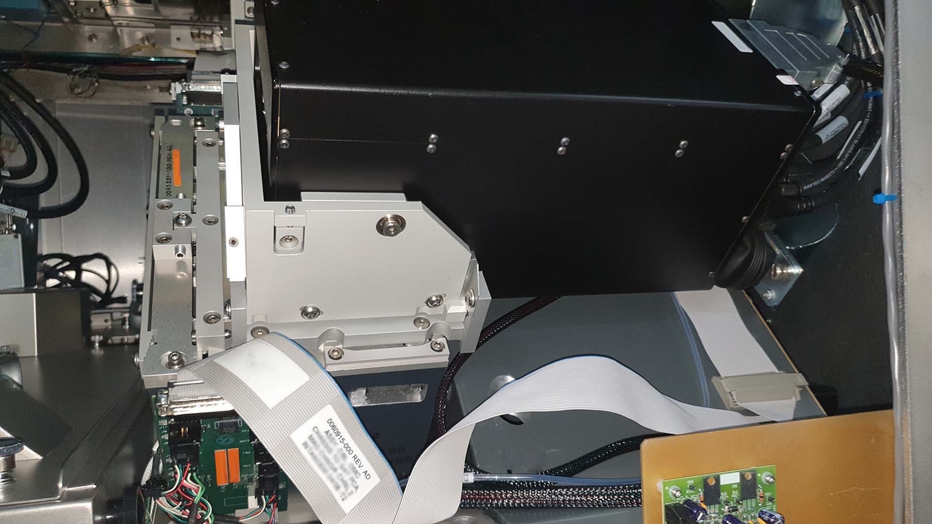
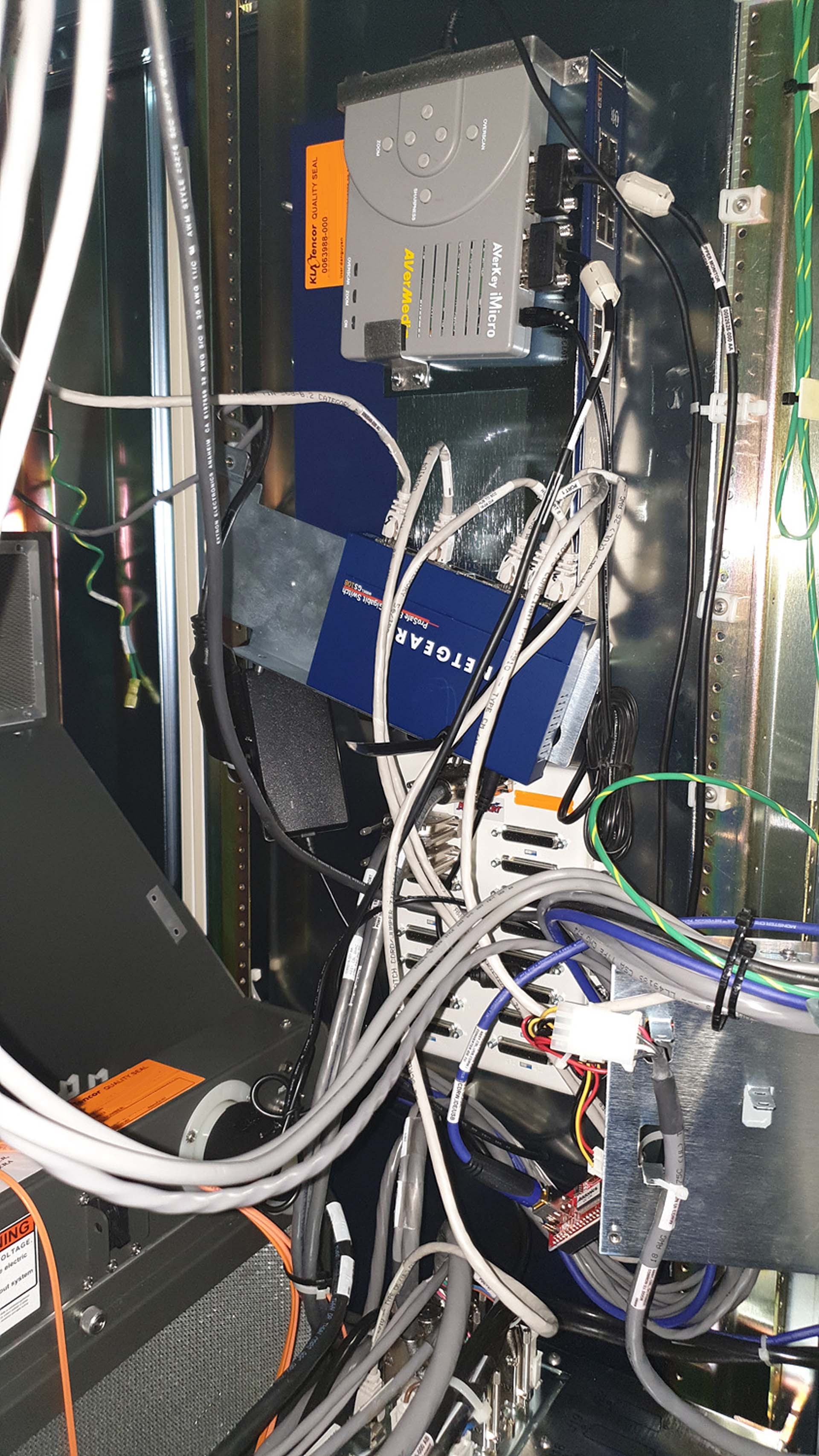
KLA / TENCOR Puma 9000 is a wafer testing and metrology equipment that ensures high accuracy in testing and analyzing semiconductor wafers. It is a fully automated system combining the best in design, technology and performance for maximum efficiency and accuracy. The unit offers high-precision tests, mapping, and measurements that can be used to optimize the performance of the integrated circuits and connectivity. KLA Puma 9000 comes with a high precision testing chamber with a specialized optical machine, including a large field of view, which enables uniform mapping of wafers for consistent results. It provides a stable environment for small-features measurement, and also is integrated with a deep-learned algorithm which helps to ensure accurate defect detection and diagnosis. Furthermore, TENCOR Puma 9000 includes a patented solution for image stitching, which allows multiple images of the same wafer to be electronically combined into one composite image. This integrated imaging technology drastically improves the accuracy of image analysis, as the high-precision measurements are taken from the full image of the wafer. In addition, Puma 9000 incorporates increasingly more powerful pixel counting software, able to count pixels, repeatable line-scans and other features of devices even as small as 5 microns. It can detect features as small as 0.3 micron, and also recognize patterns. This ensures that devices are accurately analyzed and allows for advanced measurements that are critical in semiconductor production. In summary, KLA / TENCOR Puma 9000 is a state of the art wafer testing and metrology tool that provides precision and accuracy when testing and analyzing semiconductor wafers. Itd features include a high-precision testing chamber, integrated deep-learned algorithm and image stitching technology, and pixel counting software, with capabilities to detect features as small as 0.3 micron. The asset is ideal for achieving maximum efficiency and accuracy, in order to optimize the performance of integrated circuits and connectivity.
There are no reviews yet


