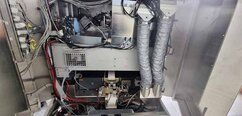
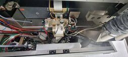
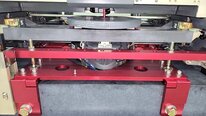
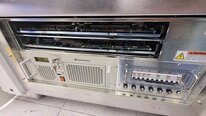
Used KLA / TENCOR Puma 9000D #9406885 for sale
URL successfully copied!
Tap to zoom
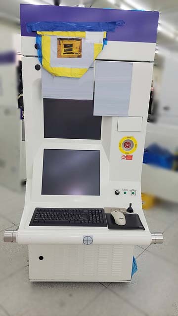

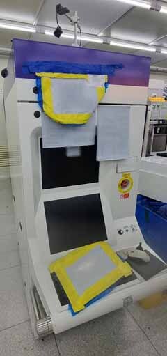

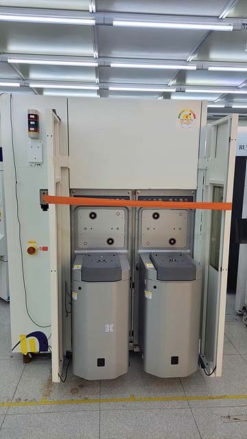

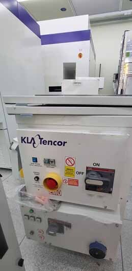


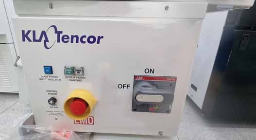

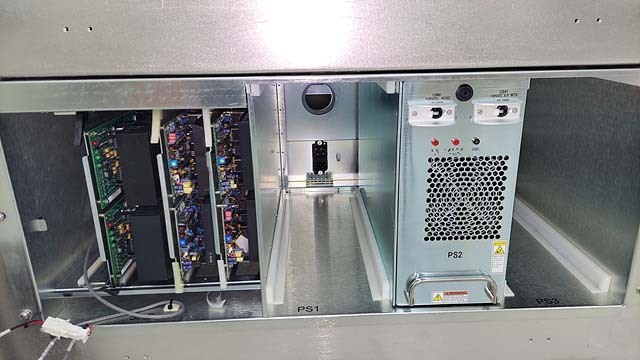

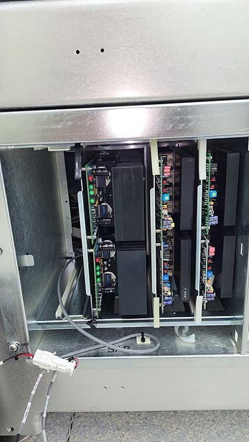

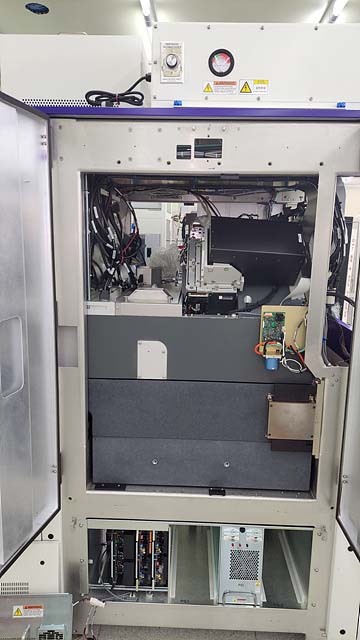

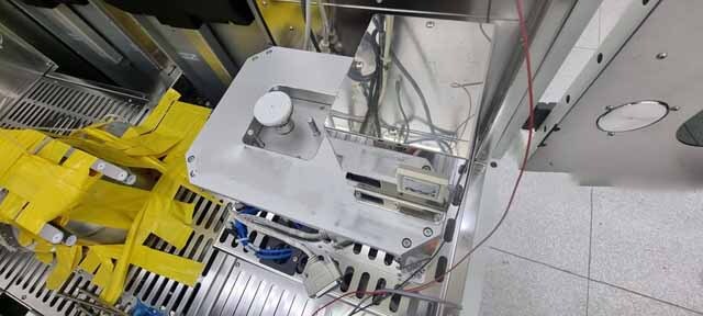

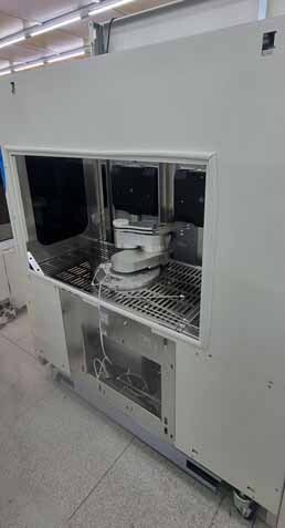

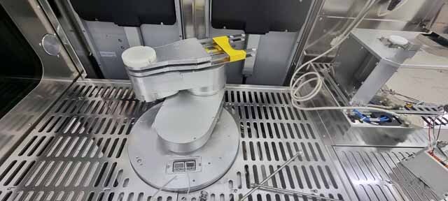

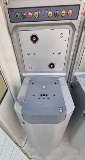

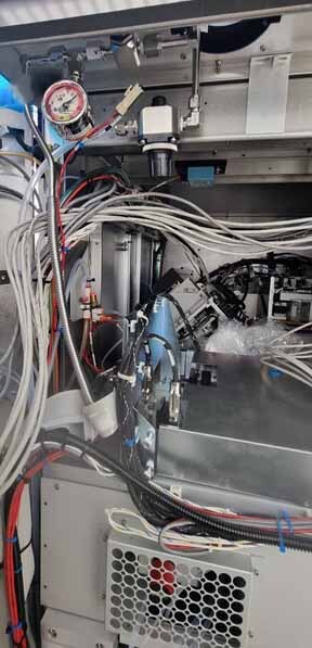

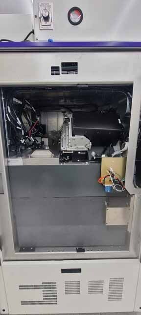

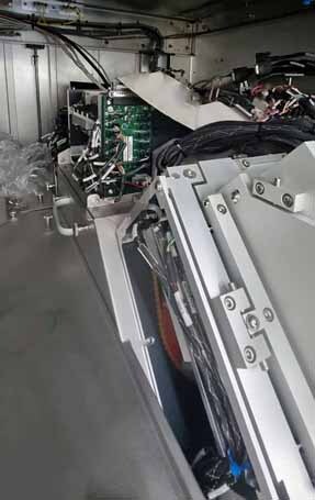

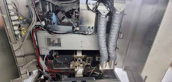


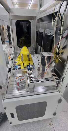

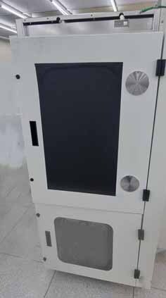

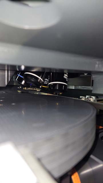

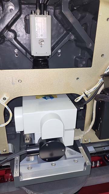

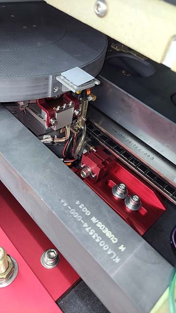

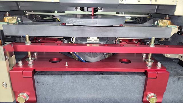

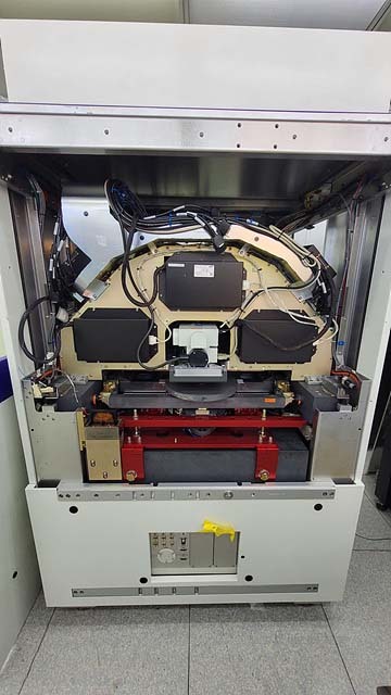

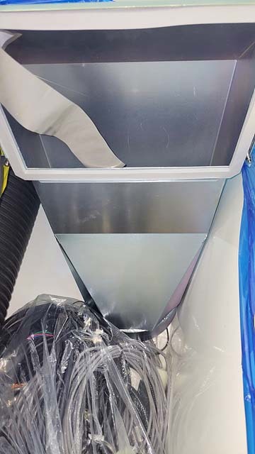





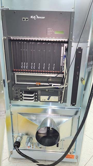

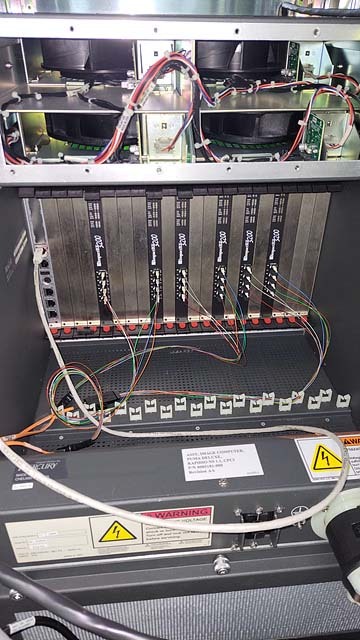

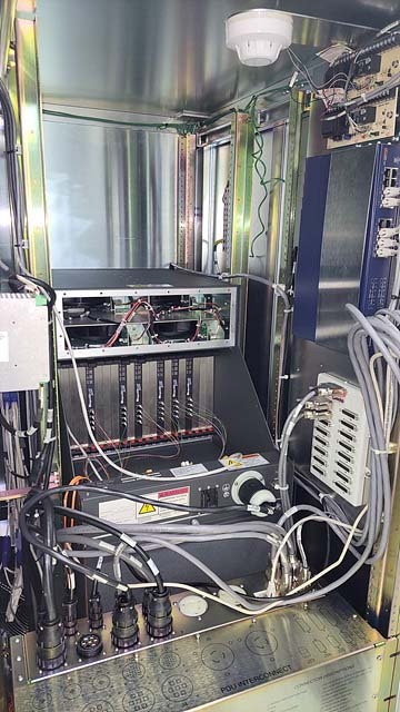

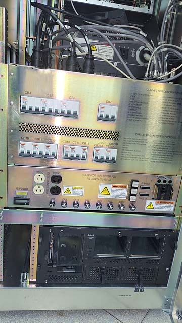

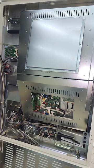

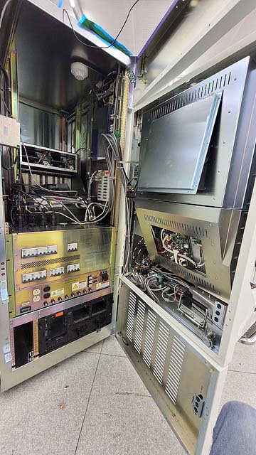

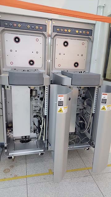

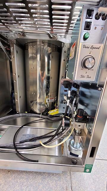





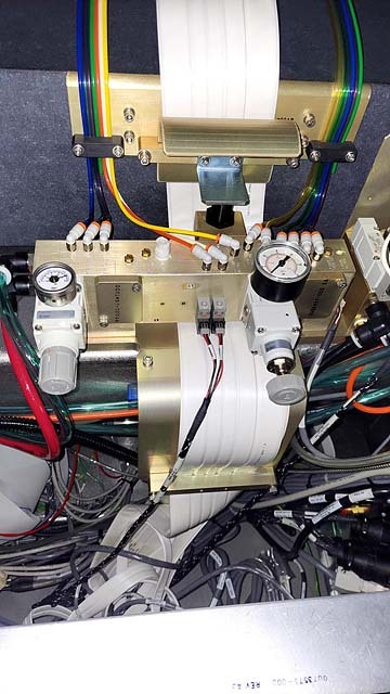

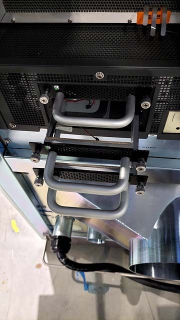


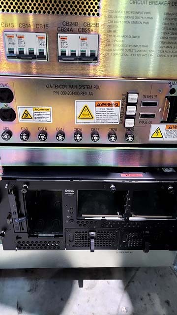

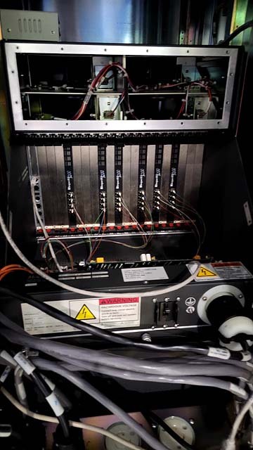

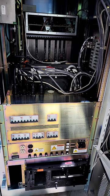

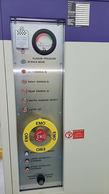

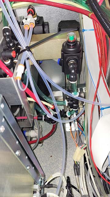

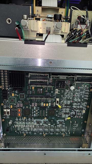

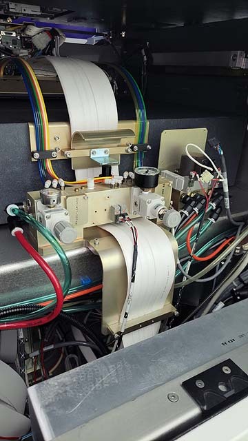

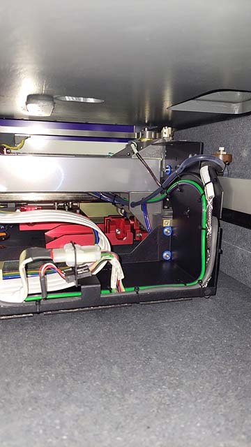


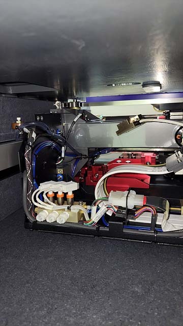

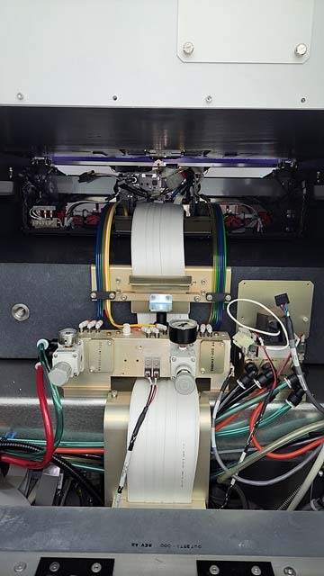


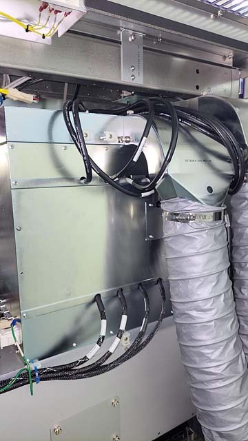

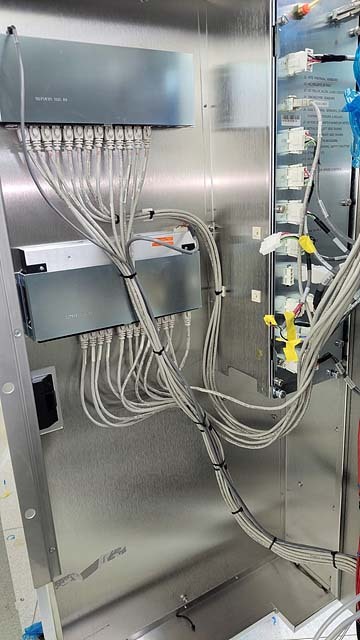

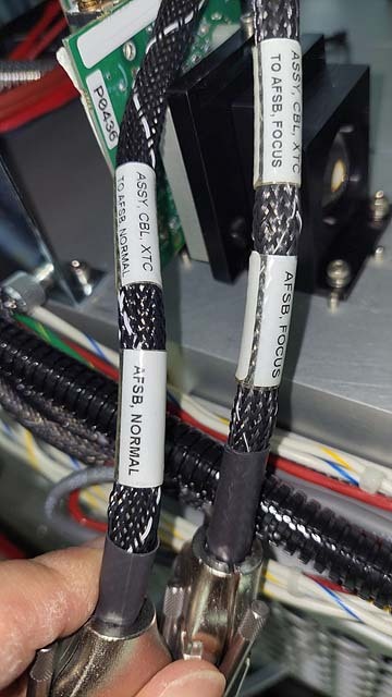

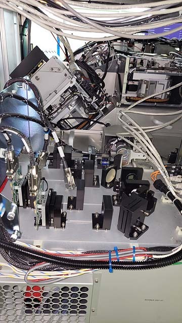

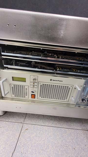

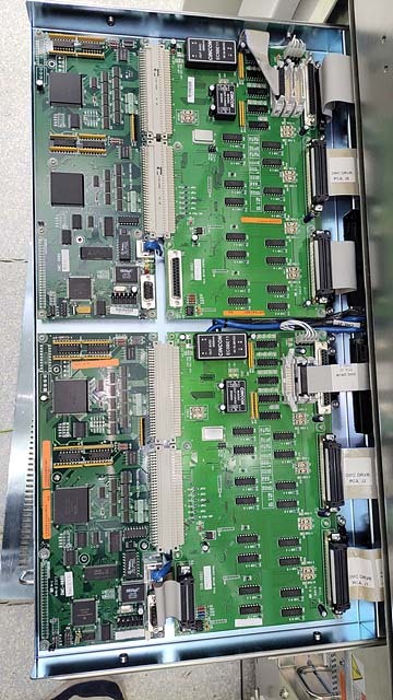


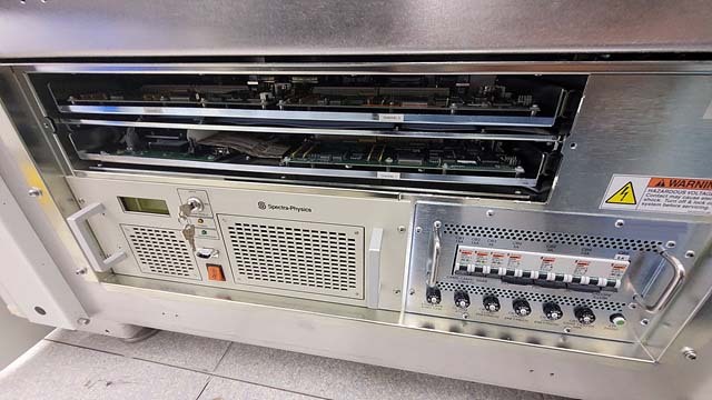

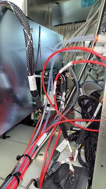

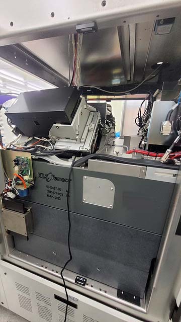

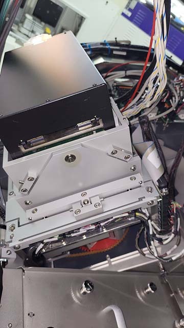

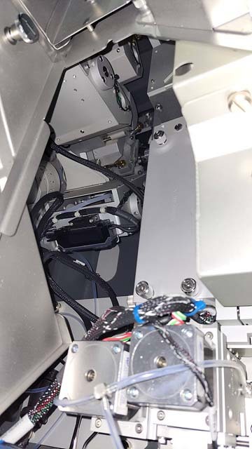

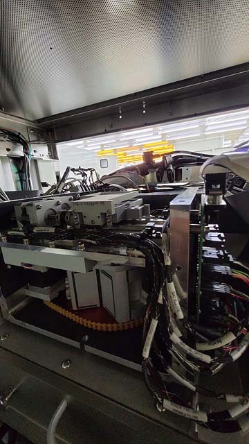


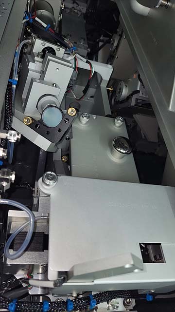

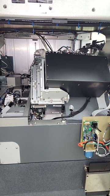

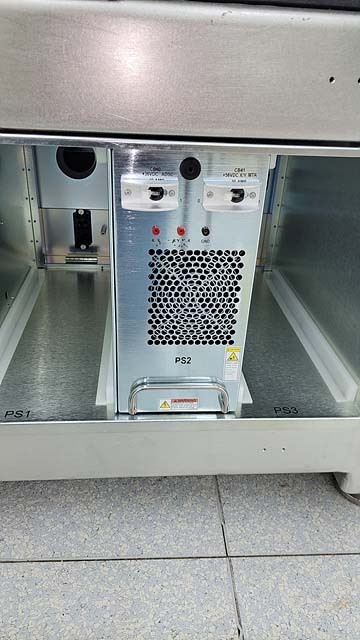

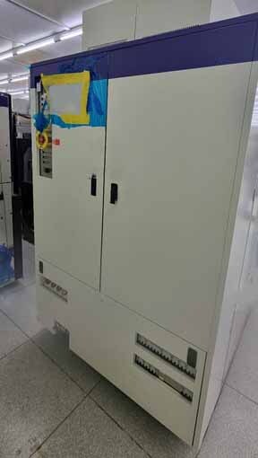

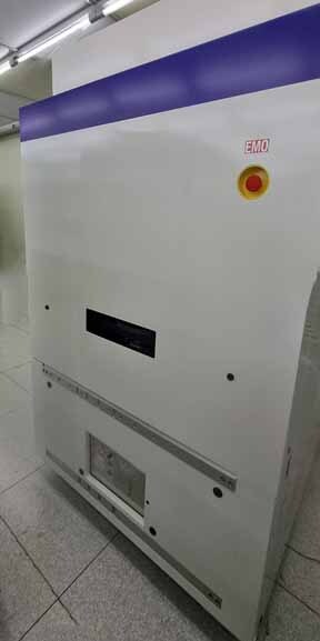

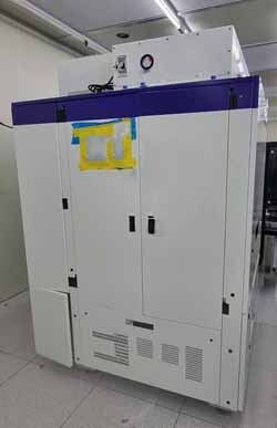

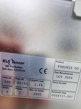

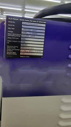

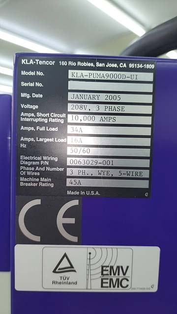

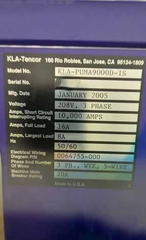

ID: 9406885
Wafer Size: 12"
Vintage: 2005
Darkfield inspection system, 12"
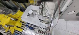
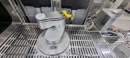
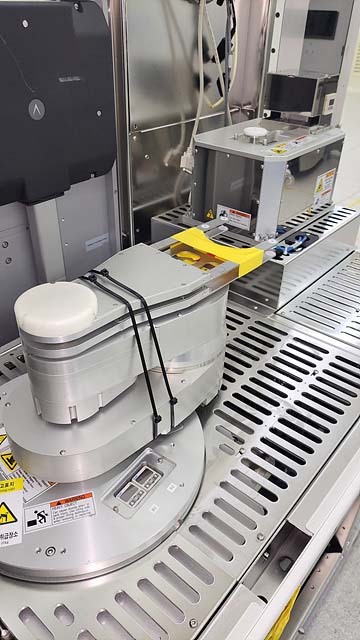
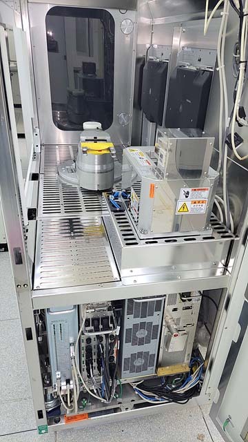
EFEM: Dual FIMS (EFEM) with Phoenix handler
GEM, SECS and HSMS
4-Color signal light tower: R,Y,G,B
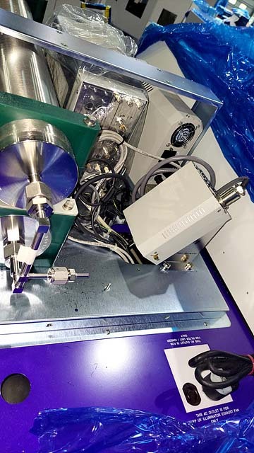
VANGUARD UV Laser head, 1W
Laser wavelength: 365nm
Selectable Scan Line (SL): SL10/15/20/40/60
(2) ISOPORT Loadports
FEC
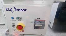
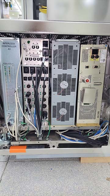
Interlock controller
ACDC Power
YASKAWA Controller
Stage:
X, Y and Theta stage installed stage locking jig
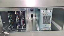
PS2 / X,Y1,Y2,ADSC Amp
SMAC and X-Flex board
2-FVPA (Rear FVPA missing)
PS1 and Z Amp missing
Optic
AF Camera
Line scan camera
CIB 1,2,3 Board
XTC Board
AF Unit
AFSB
Focus missing
CH2 Line scan camera missing
Laser power supply
Laser head
Galil board (3-Channels)
User interface:
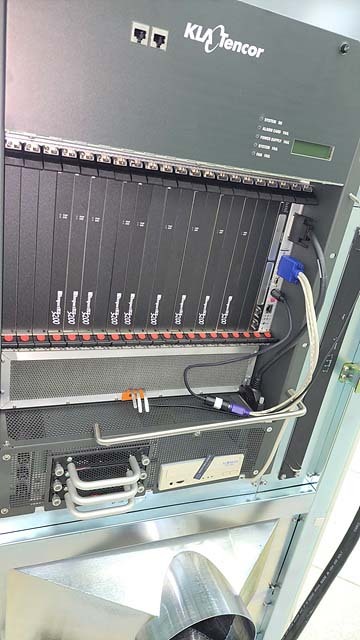
IMC System (Mercury and host PC)
SCC (HDD Missing)
Monitor
Keyboard
Joystick
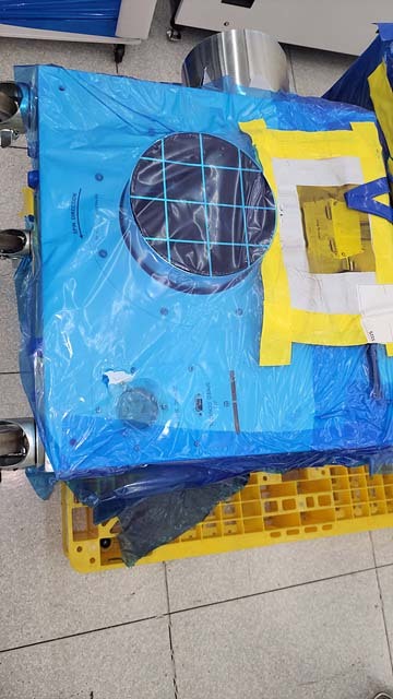
Blower box
Line conditioner
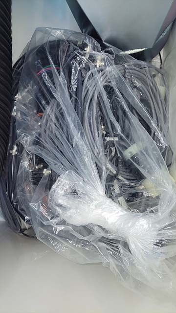
UI and IS Connected cable
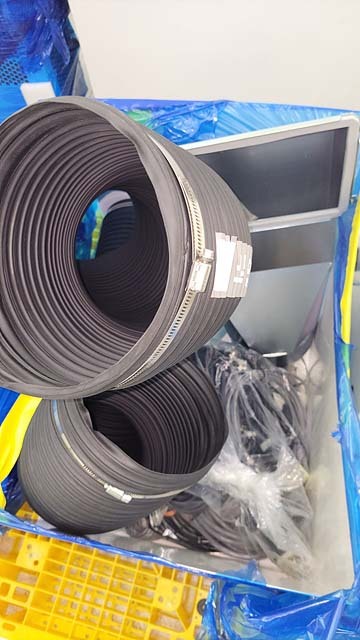
Exhaust hose
2005 vintage.
KLA / TENCOR Puma 9000D is a wafer testing and metrology equipment that provides high-performance optical and automated inspection. This system is specifically designed to deliver high accuracy and precision measurements for advanced 3D device characterization. It offers micron-level resolution with exceptional signal to noise ratios, making it increasingly reliable for inspection in the semiconductor industry. At the core of this unit is its advanced optical metrology capabilities. A dual-wavelength spectrometer uses a wide range of light sources to measure device parameters such as thickness, optical properties, and flatness at multiple points on the surface of the wafer. The spectrometer utilizes line scanning and multiple diffractometers to detect features with extreme resolution and accuracy. Additionally, the spectrometer is equipped with an automated route plan, making it easy to create surface profiles of any wafer quickly and accurately. KLA Puma 9000D also features advanced automated inspection. A high-resolution 3D imaging machine utilizes refraction and reflection tools to detect minute features on the surface of the wafer. The 3D imaging tool is used to measure a variety of device parameters, including line widths, aspect ratios, hole depths, and thermal stress. Additionally, this asset is equipped with an automated defect review analyzer that can detect and report small surface defects that may be invisible to the naked eye. In addition to these capabilities, TENCOR PUMA 9000 D also includes several advanced software features that are designed to increase user-efficiency. The model includes a sophisticated defect feature mapping program that can present device data in a variety of formats. The software can also access a large library of defect algorithms that allow for accurate and repeatable measurements. This can help reduce inspection times and improve accuracy. Puma 9000D is an extremely advanced equipment that is designed to provide high-performance inspection services. Its advanced optical and automated inspection capabilities allow for reliable and accurate measurements at a micron level. Additionally, the software features are powerful and user-friendly, making it easy to analyze and interpret data. With its advanced features, PUMA 9000 D is ideal for a wide range of applications in the semiconductor industry.
There are no reviews yet


