Used KLA / TENCOR UV 1050 #293752938 for sale
URL successfully copied!
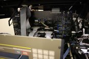
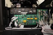
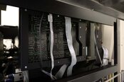
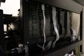
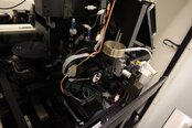
Tap to zoom

ID: 293752938
Wafer Size: 6"-8"
Vintage: 1992
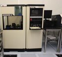
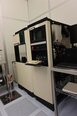
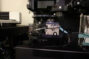
Film thickness measurement system, 6"-8"
1992 vintage.
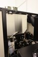
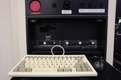
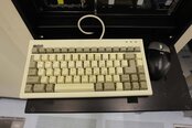
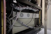
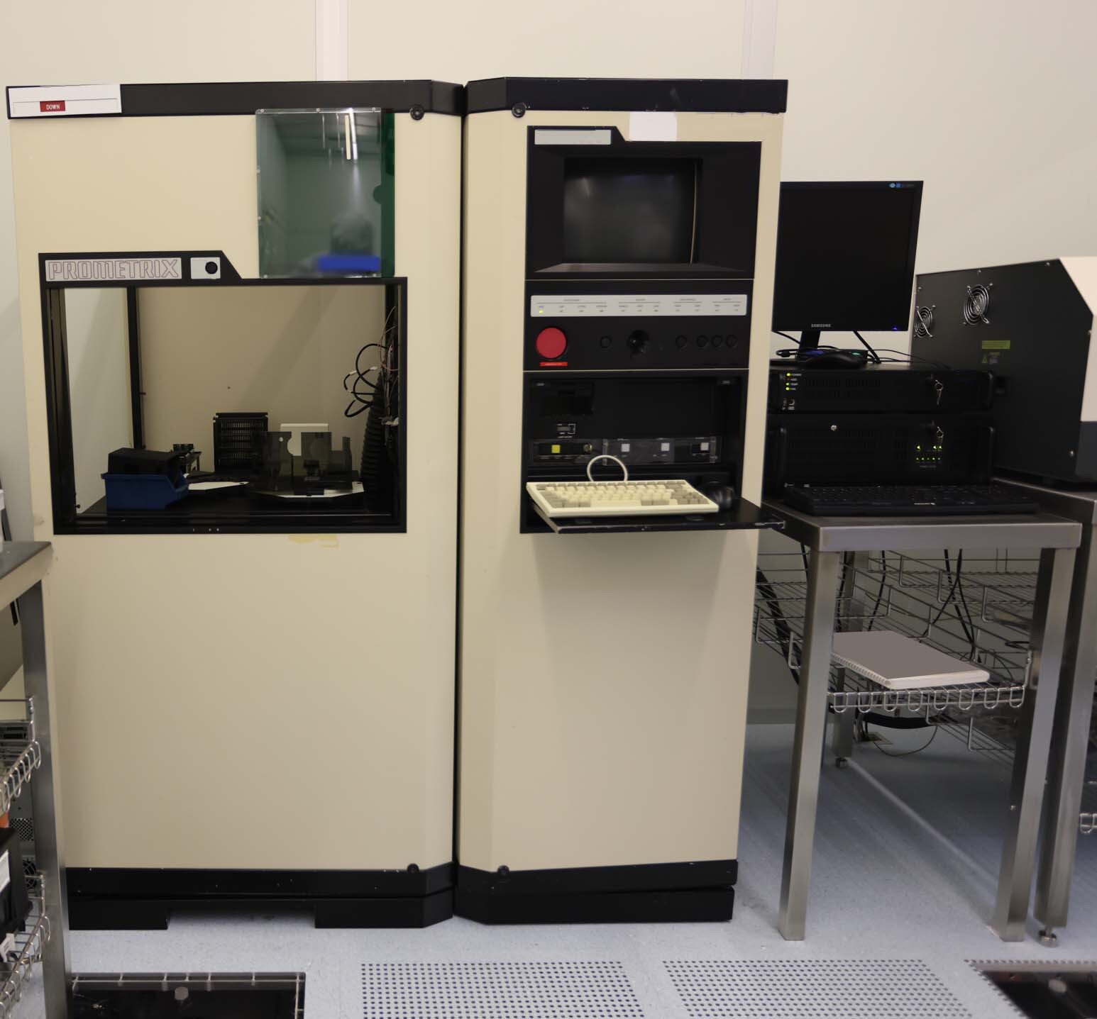
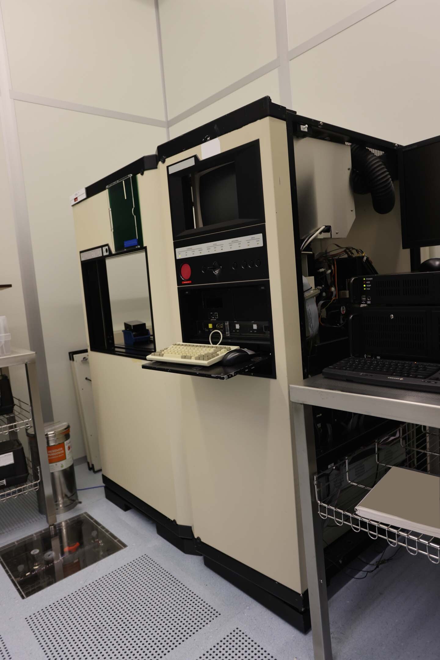
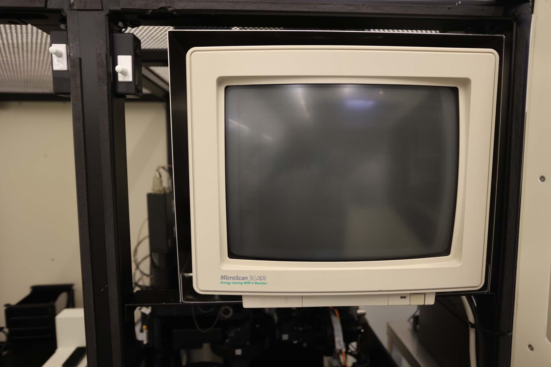
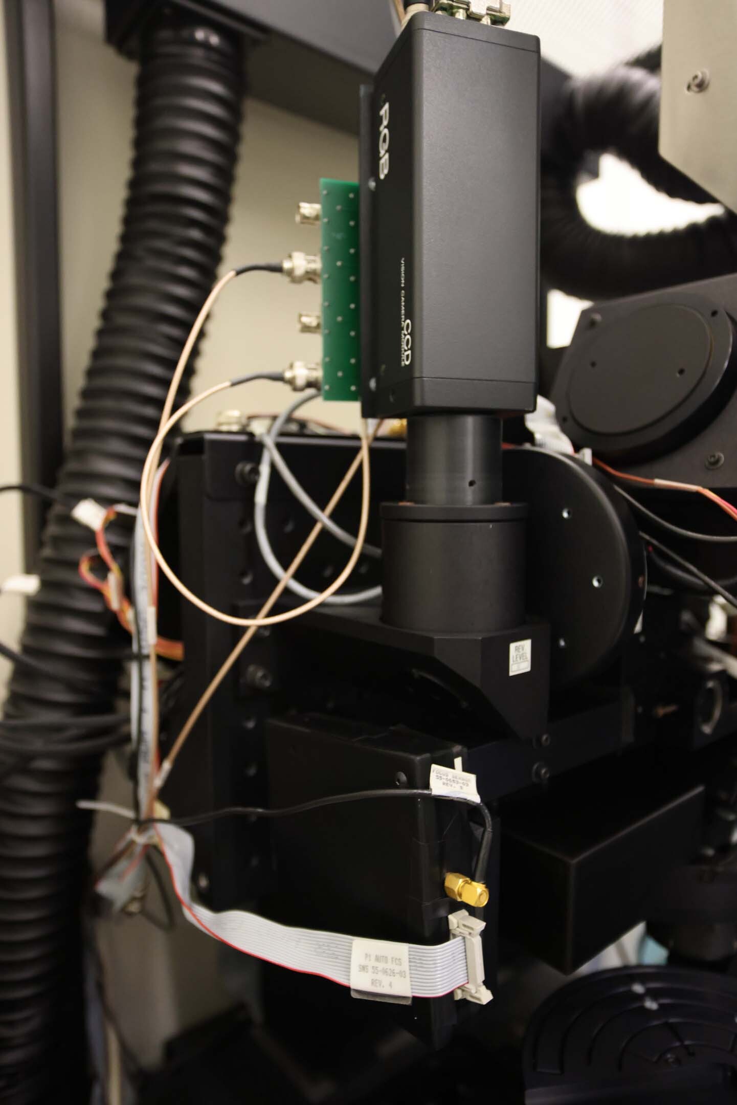
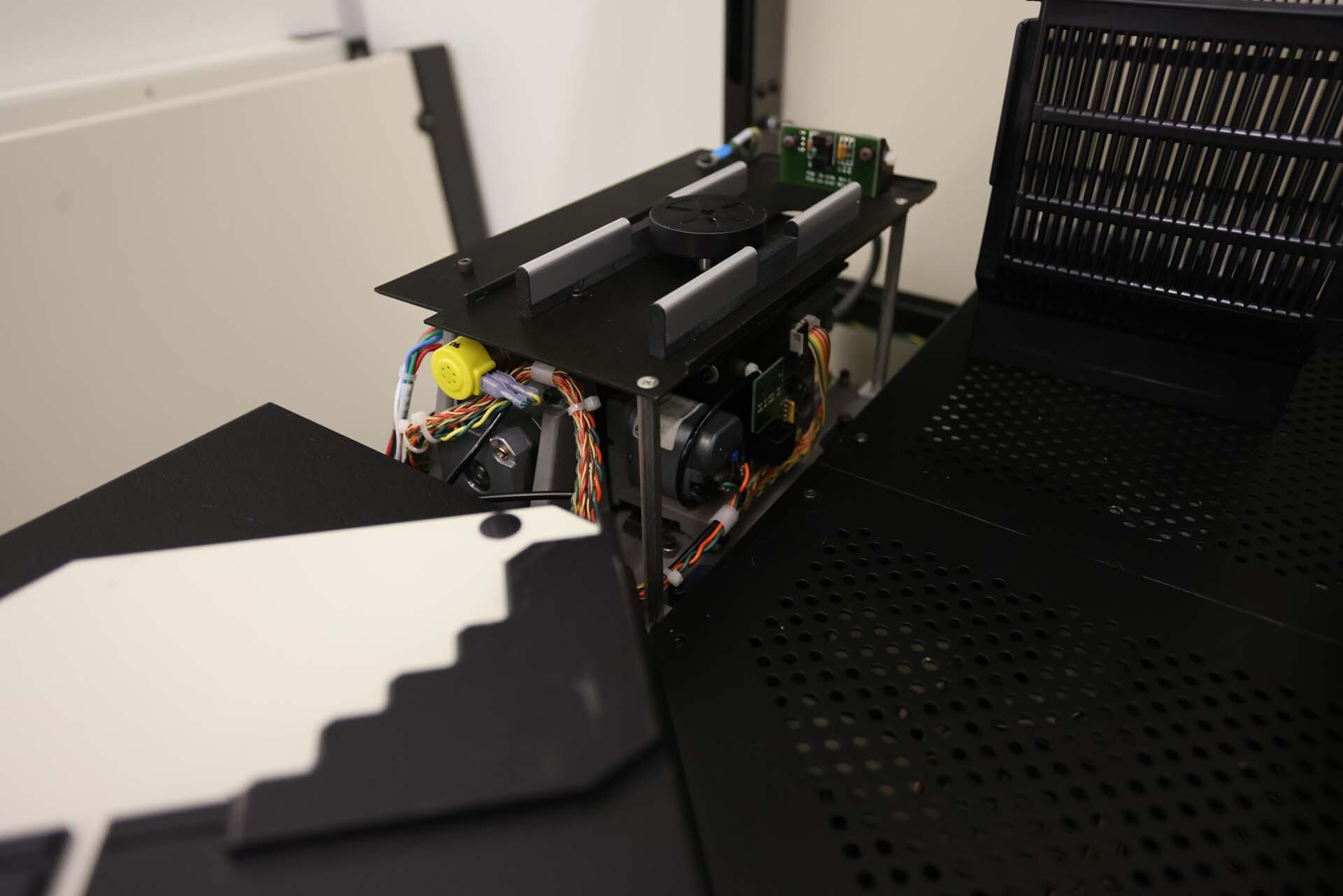
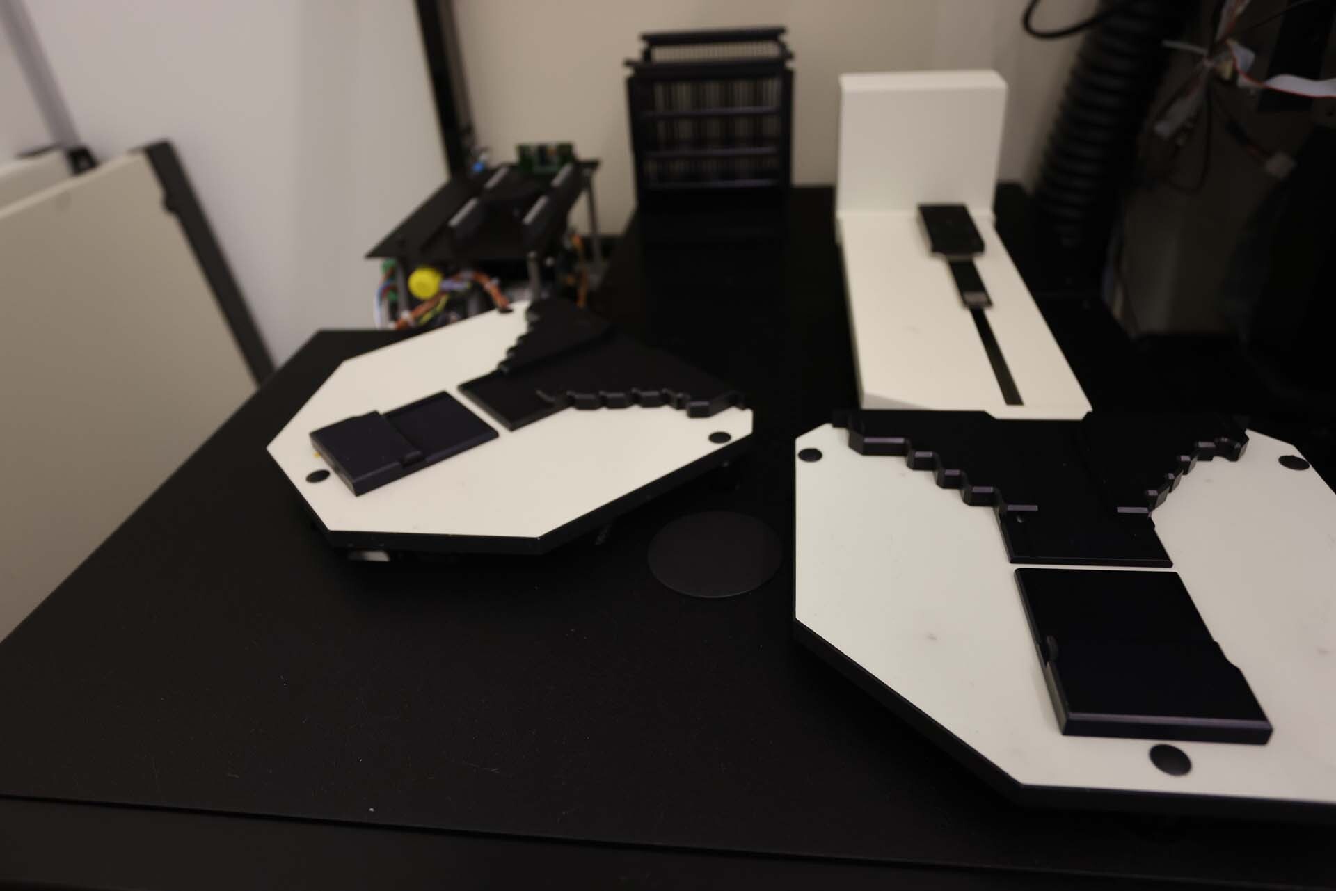
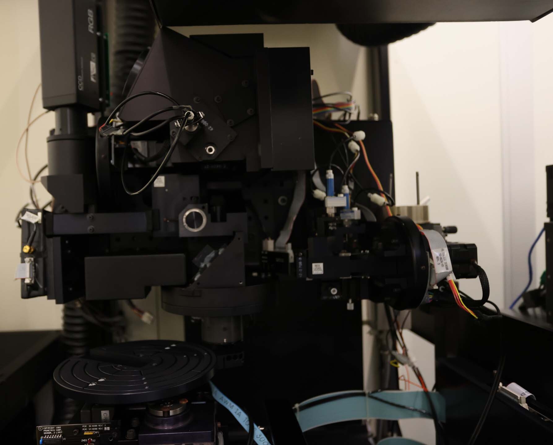
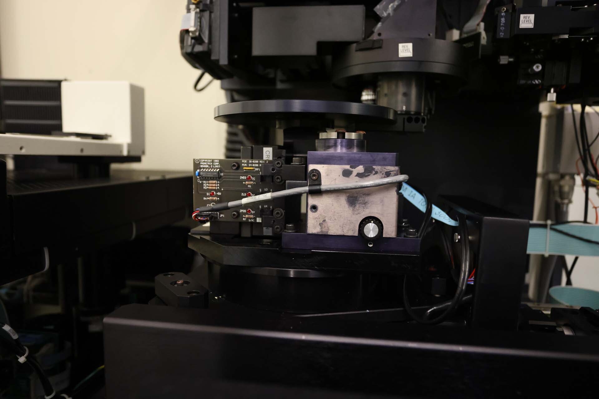
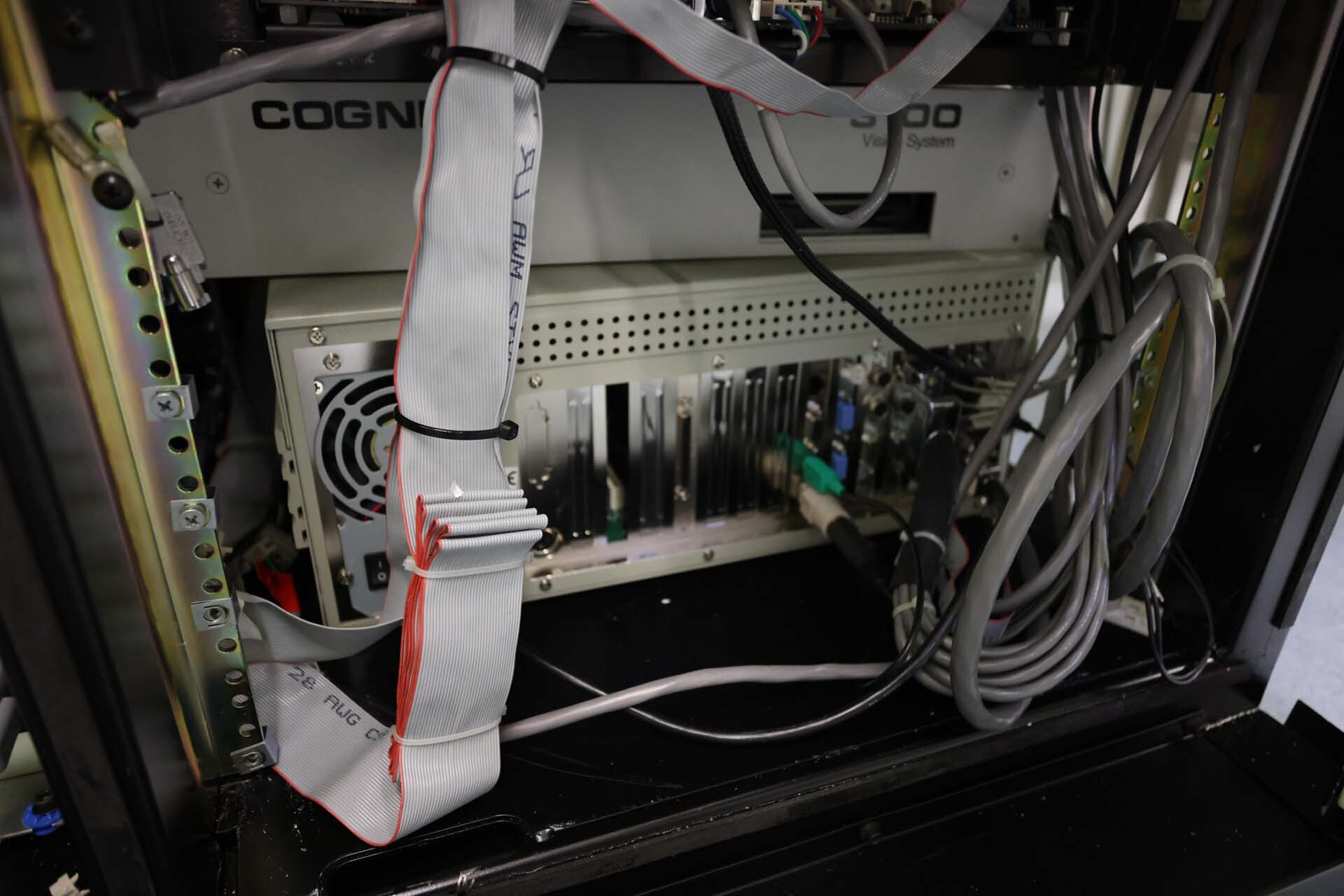
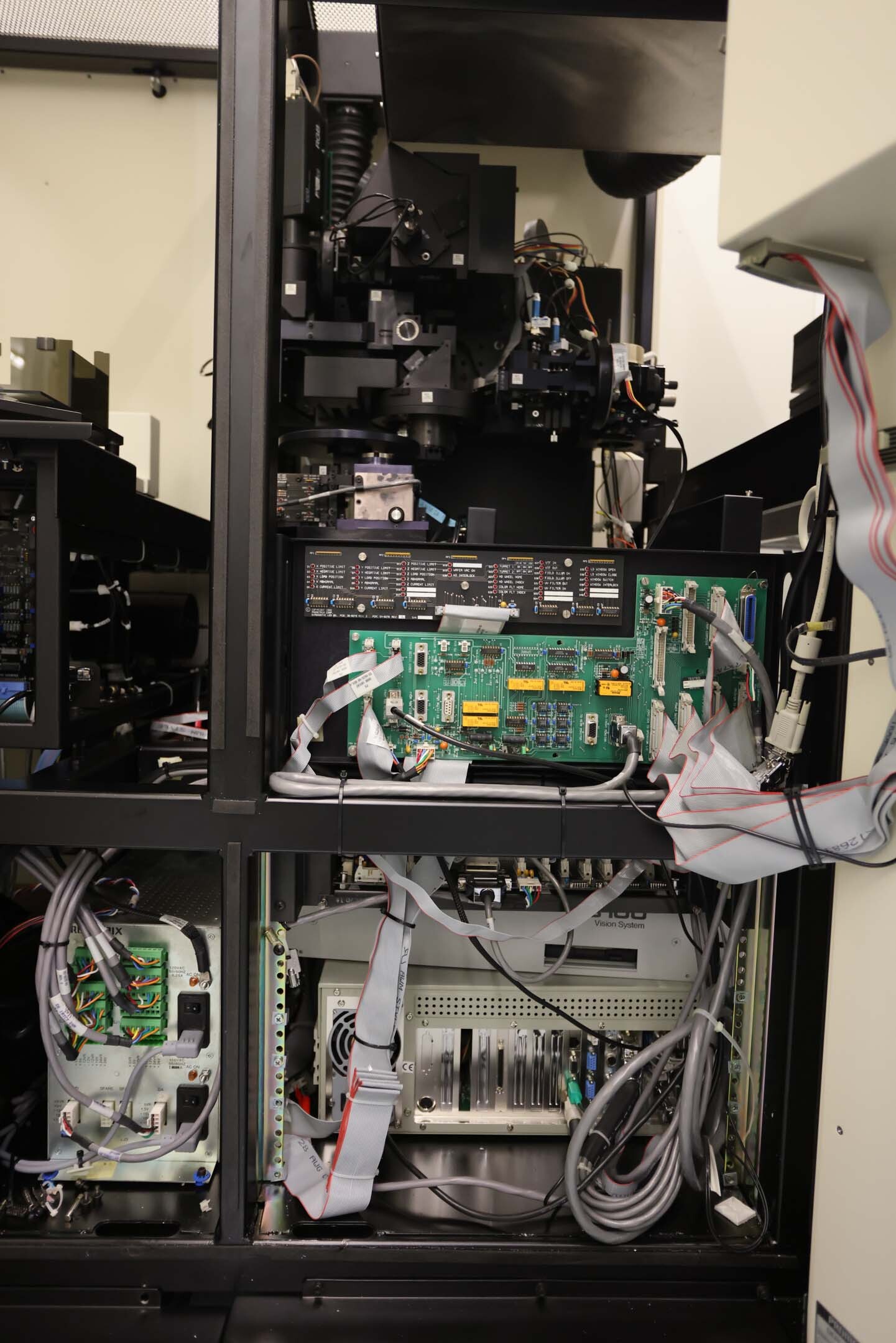
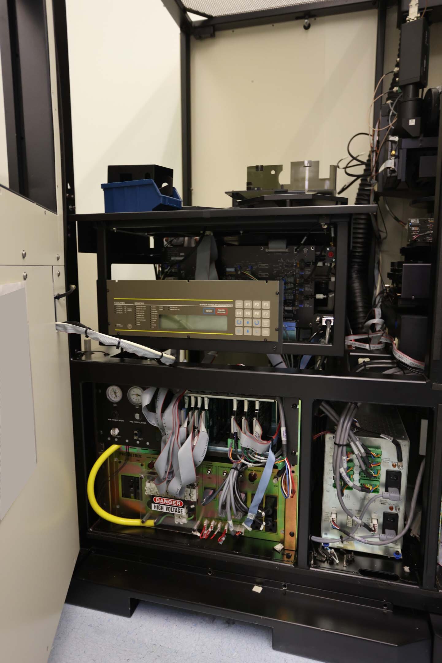
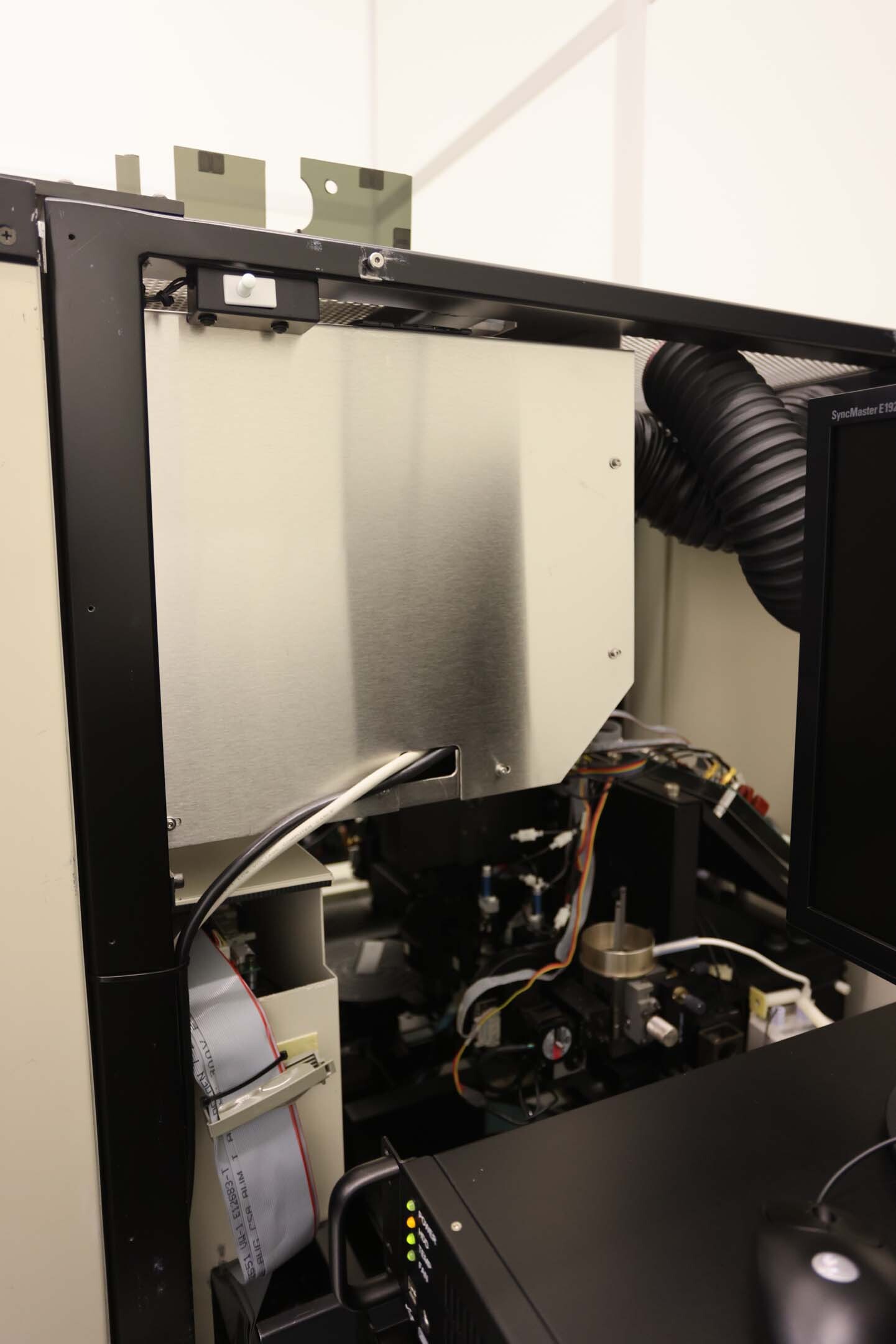
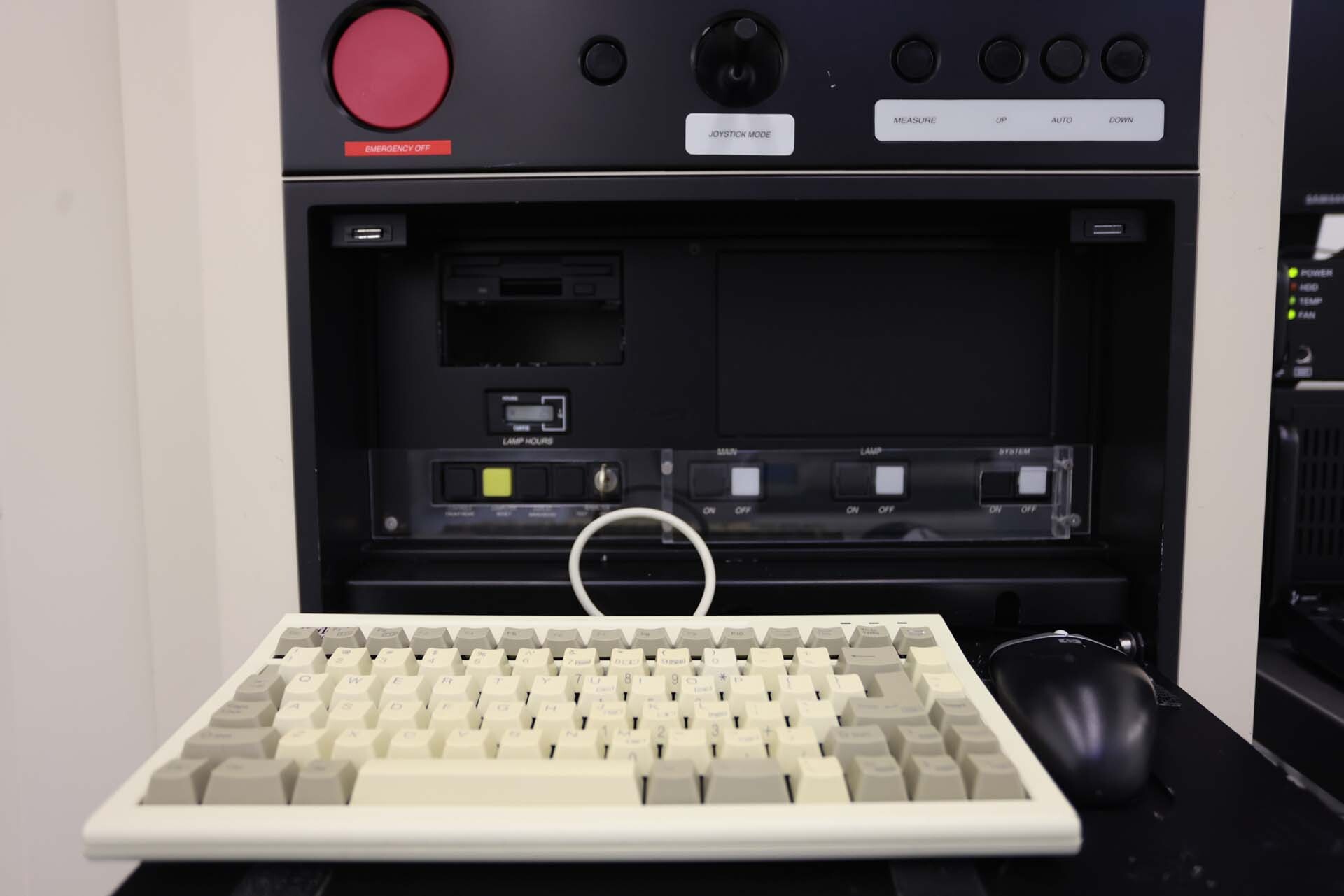
KLA / TENCOR UV 1050 is a high-end wafer testing and metrology equipment designed for the semiconductor industry. This system provides quick and precise testing of wafer thinning and layer quality with the ability to detect point defects, wafer warping, and surface roughness of bare and coated semiconductor wafers. The unit is composed of two main components: the patic KLA UV 1050 laser interferometry machine and the serviceable subsystems. TENCOR UV 1050 tool utilizes a precision laser, optics, and electronics to precisely measure the thickness and total height of the wafer. The asset consists of two laser interferometer heads, each with a unique beam configuration, that are used to measure the wafer's amount topography by recording its maximum point-to-point thickness variation and total height of the wafer plus any overcoat material. It is equipped with inherent non-contact 3-channel optical measurement technology that can measure a wide range of wafer thicknesses over a wide range of incidence angles. This model can also detect nanometer-scale particles on the wafer surface. Additionally, a step-by-step calibration process is used to ensure accurate measurements. The serviceable subsystems are designed to support UV 1050 equipment and include a programmable computer for controlling the system, a raster imaging subsystem to track the wafer position as it passes through the interferometer, and a zither leveling subsystem to level the wafer's surface as it passes through the head. The unit is also designed to provide quick and easy maintenance including automated diagnostics, and a machine calibration for optimal performance. KLA / TENCOR UV 1050 tool offers many advantages for wafer testing and metrology. It ensures precise and repeatable measurements of wafer thinning and layer quality, and is designed to detect point defects, wafer warping, and surface roughness. The user-friendly interface makes it easy to operate and maintain, while the serviceable subsystems provide support for accurate and reliable testing. Additionally, the asset's flexible configurations can be customized to meet specific testing needs. Ultimately, KLA UV 1050 wafer testing and metrology model is an ideal solution for precision wafer testing in the semiconductor industry.
There are no reviews yet