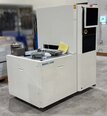
Used KLA / TENCOR UV 1080 #293756631 for sale
URL successfully copied!
Tap to zoom

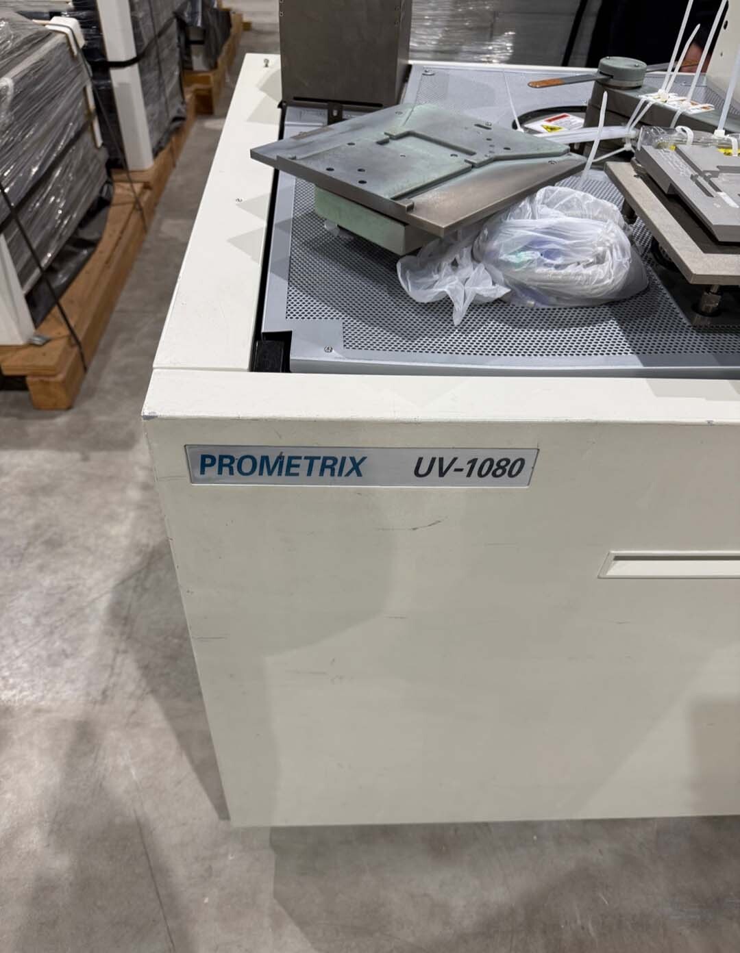
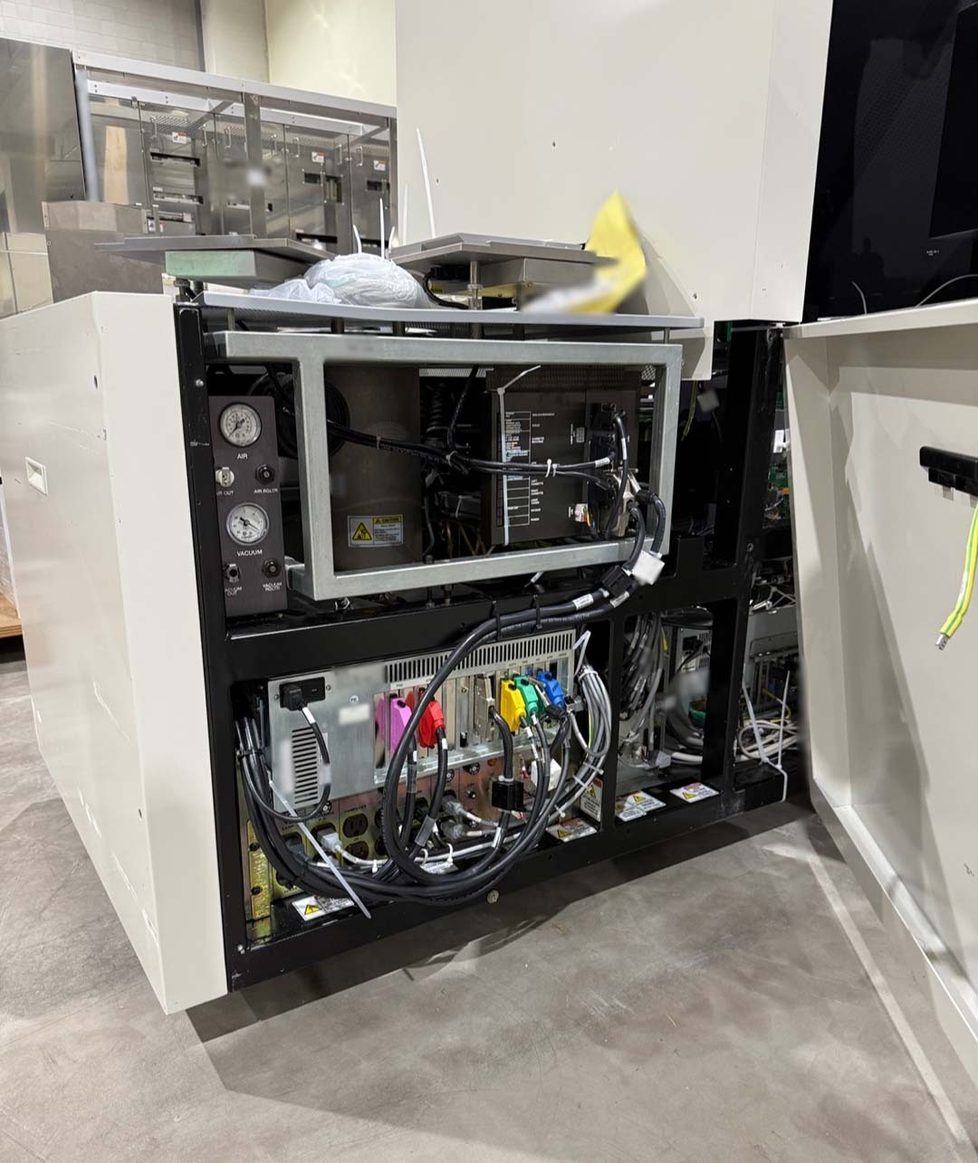
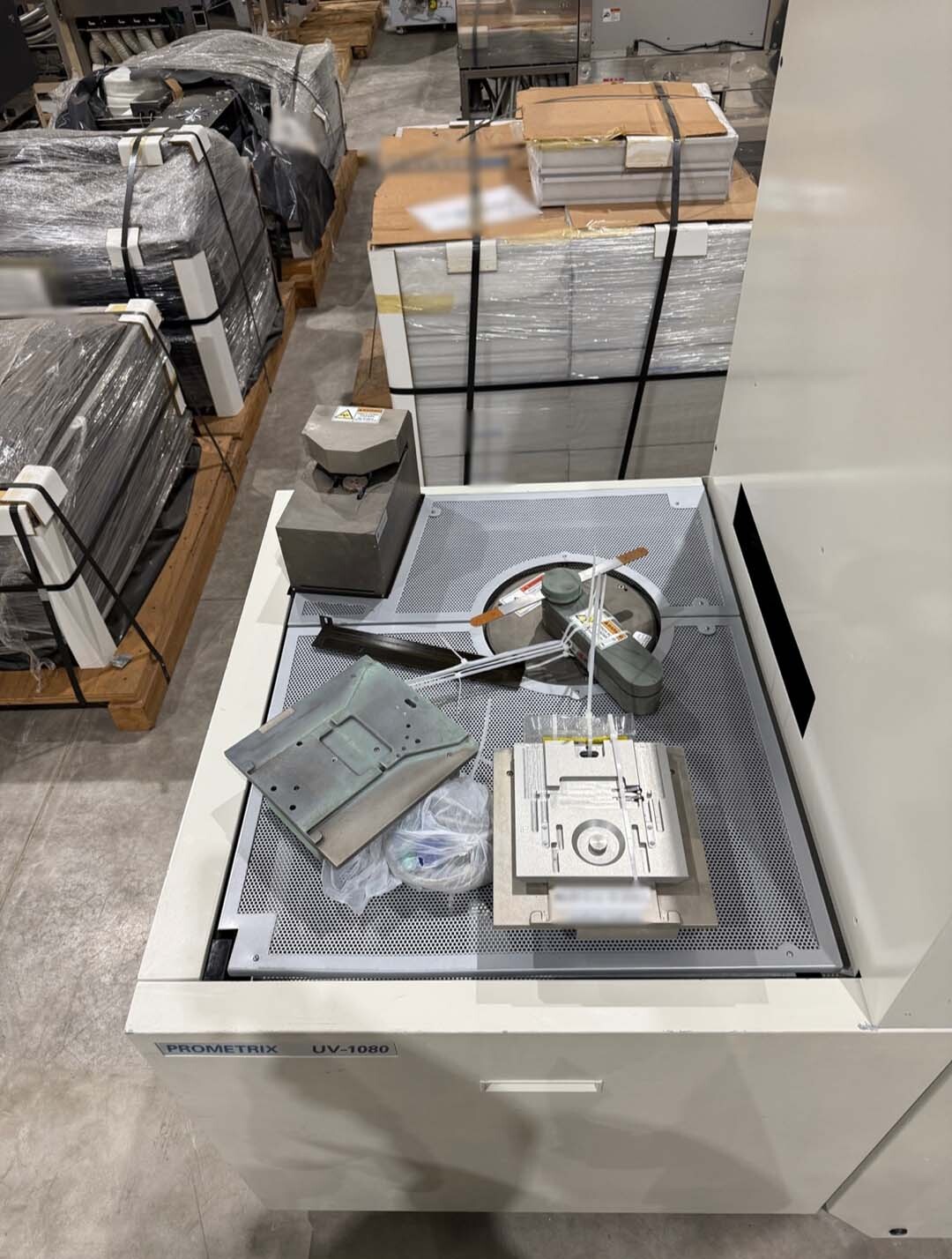
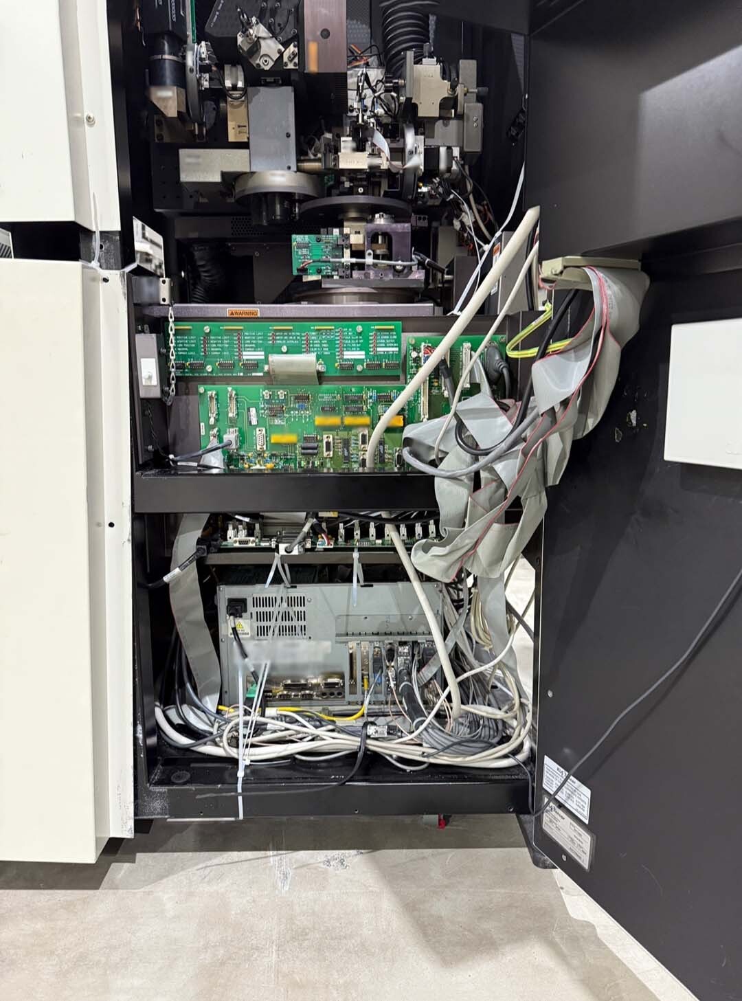
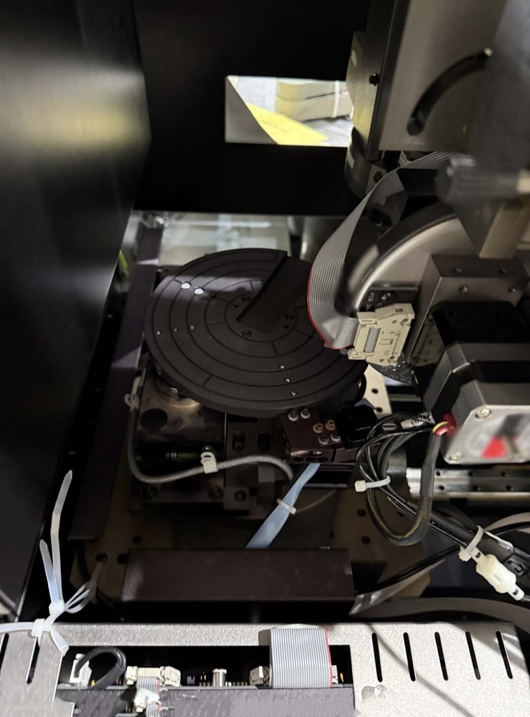
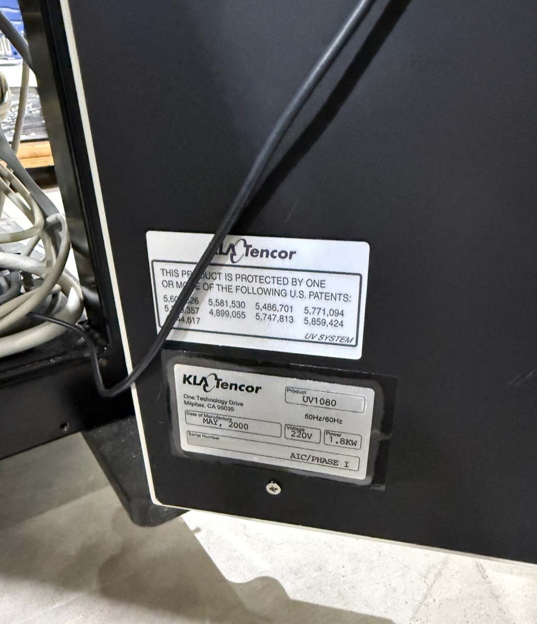
ID: 293756631
Wafer Size: 6"-8"
Vintage: 2000
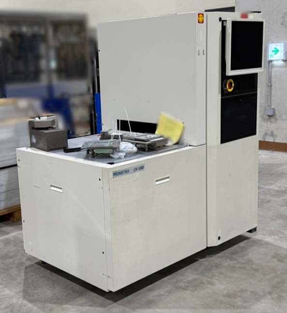
Film thickness measurement system, 6"-8"
2000 vintage.
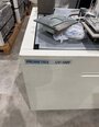
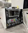
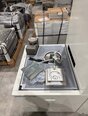
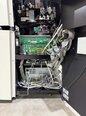
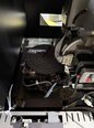
KLA / TENCOR UV 1080 is a cutting-edge wafer testing and metrology equipment utilized in the semiconductor industry for inspecting and measuring critical features of semiconductor wafers. This advanced system integrates state-of-the-art UV optical technology with sophisticated algorithms to provide superior accuracy and efficiency in detecting defects and assessing wafer quality. At the core of KLA UV 1080 unit is its UV illumination source, which emits ultraviolet light onto the wafer surface. This UV light interacts with the wafer's materials, causing various features and defects to become visible and detectable. The machine's high-intensity UV source ensures optimal contrast and resolution, enabling the detection of sub-micron defects with exceptional sensitivity. TENCOR UV 1080 tool features a precision stage capable of accurately positioning the wafer under the UV illumination source for thorough inspection. The stage can move in multiple axes, allowing for comprehensive scanning of the wafer surface to capture defects and anomalies from all angles. The asset's advanced stage control mechanisms ensure precise and repeatable positioning, enhancing the model's overall reliability and performance. To analyze the information captured from the wafer surface, UV 1080 equipment employs sophisticated detection algorithms and image processing techniques. These algorithms enhance the system's ability to differentiate between actual defects and benign variations in the wafer's features, ensuring accurate defect classification and minimizing false alarms. The unit can analyze large volumes of data rapidly, enabling high-throughput and efficient wafer inspection processes. KLA / TENCOR UV 1080 machine is equipped with a high-resolution imaging tool that captures detailed images of the wafer surface with exceptional clarity and precision. The asset's imaging capabilities enable the visualization of minute defects and subtle variations in the wafer's topography, facilitating comprehensive defect detection and characterization. The high-quality images generated by the model provide valuable insights into the wafer's quality and help identify areas that require further investigation or improvement. In addition to defect detection, KLA UV 1080 equipment offers advanced metrology capabilities for measuring critical parameters of semiconductor wafers. The system can accurately assess dimensions, thickness, and other key characteristics of wafer structures, providing valuable data for process control and optimization. By combining defect inspection with metrology functionalities, TENCOR UV 1080 unit enables comprehensive quality assessment and yield enhancement in semiconductor manufacturing. Overall, UV 1080 machine represents a state-of-the-art solution for wafer testing and metrology in the semiconductor industry. With its advanced UV optical technology, precision stage control, sophisticated algorithms, high-resolution imaging, and comprehensive metrology capabilities, the tool offers superior performance, accuracy, and efficiency in detecting defects and analyzing wafer quality. By leveraging the capabilities of KLA / TENCOR UV 1080 asset, semiconductor manufacturers can achieve higher yields, improve process control, and enhance overall product quality in their manufacturing operations.
There are no reviews yet