Used KLA / TENCOR UV 1250SE #293654440 for sale
URL successfully copied!
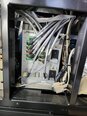
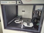
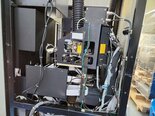
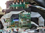
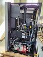
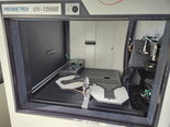
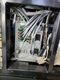
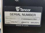
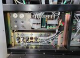
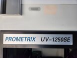
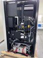
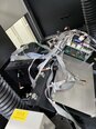
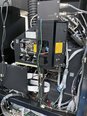
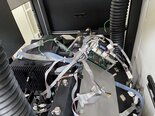
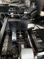
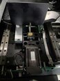
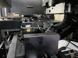
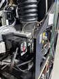
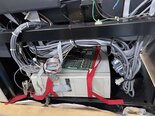
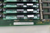
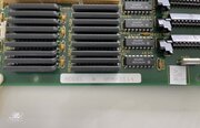
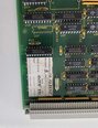
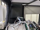
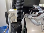
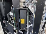
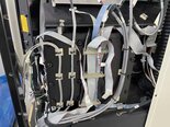
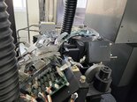
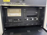
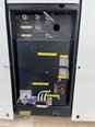
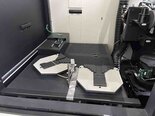

Tap to zoom
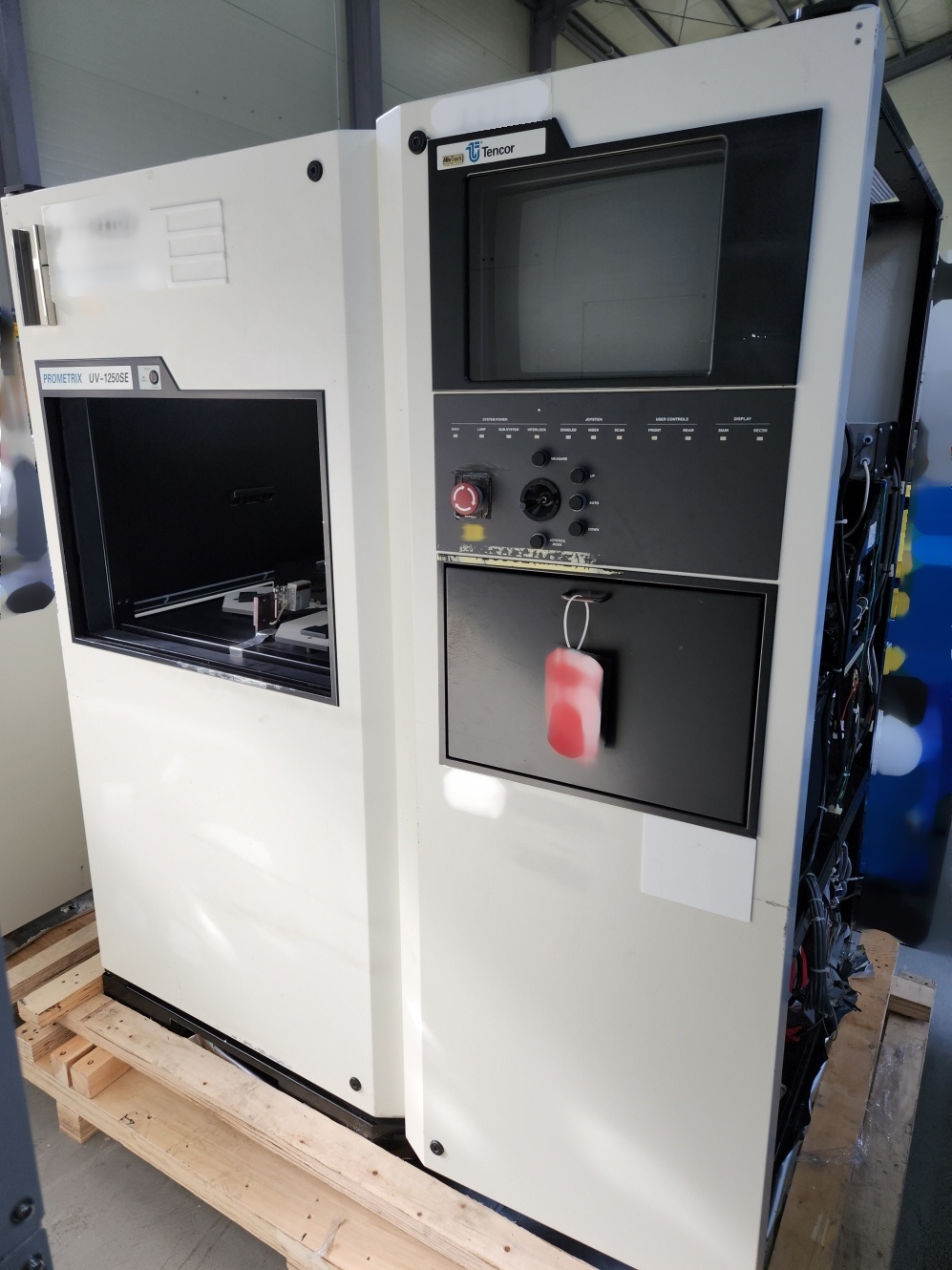

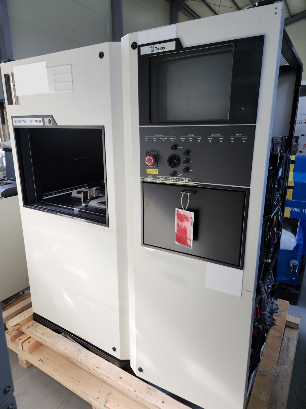
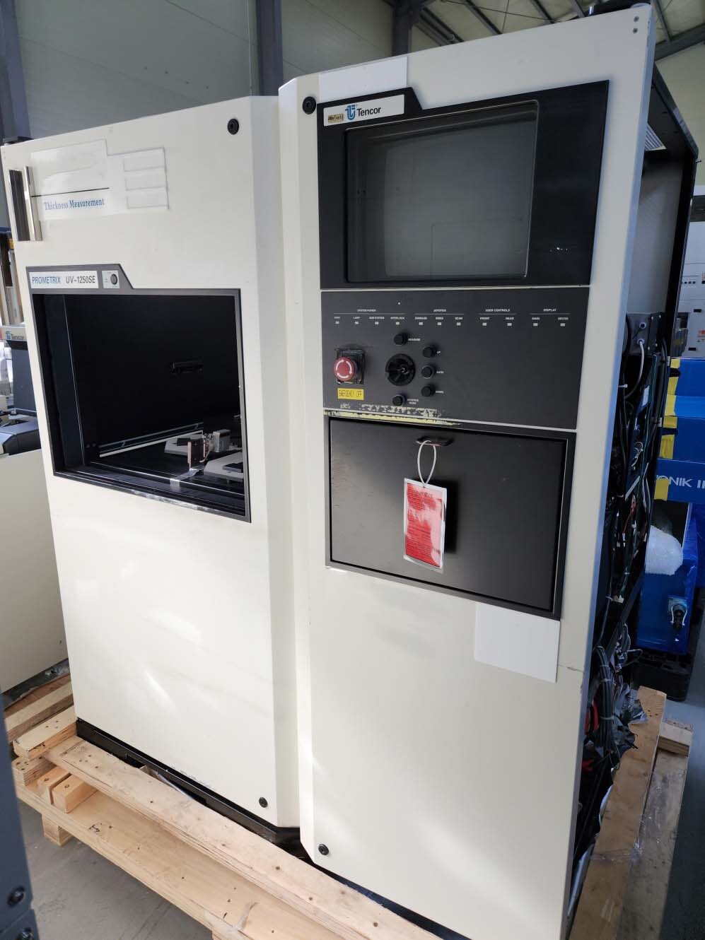
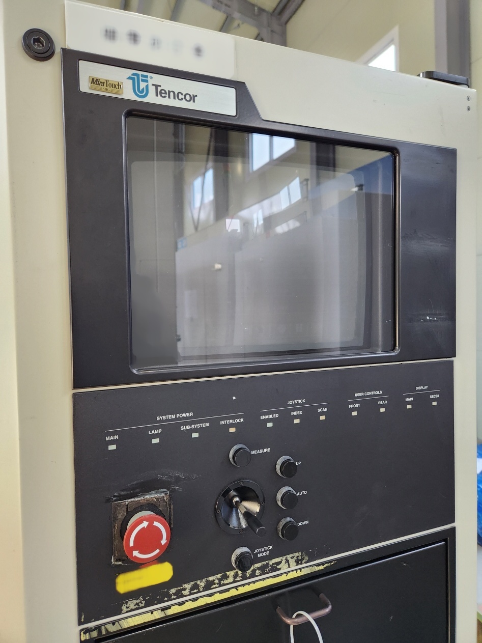
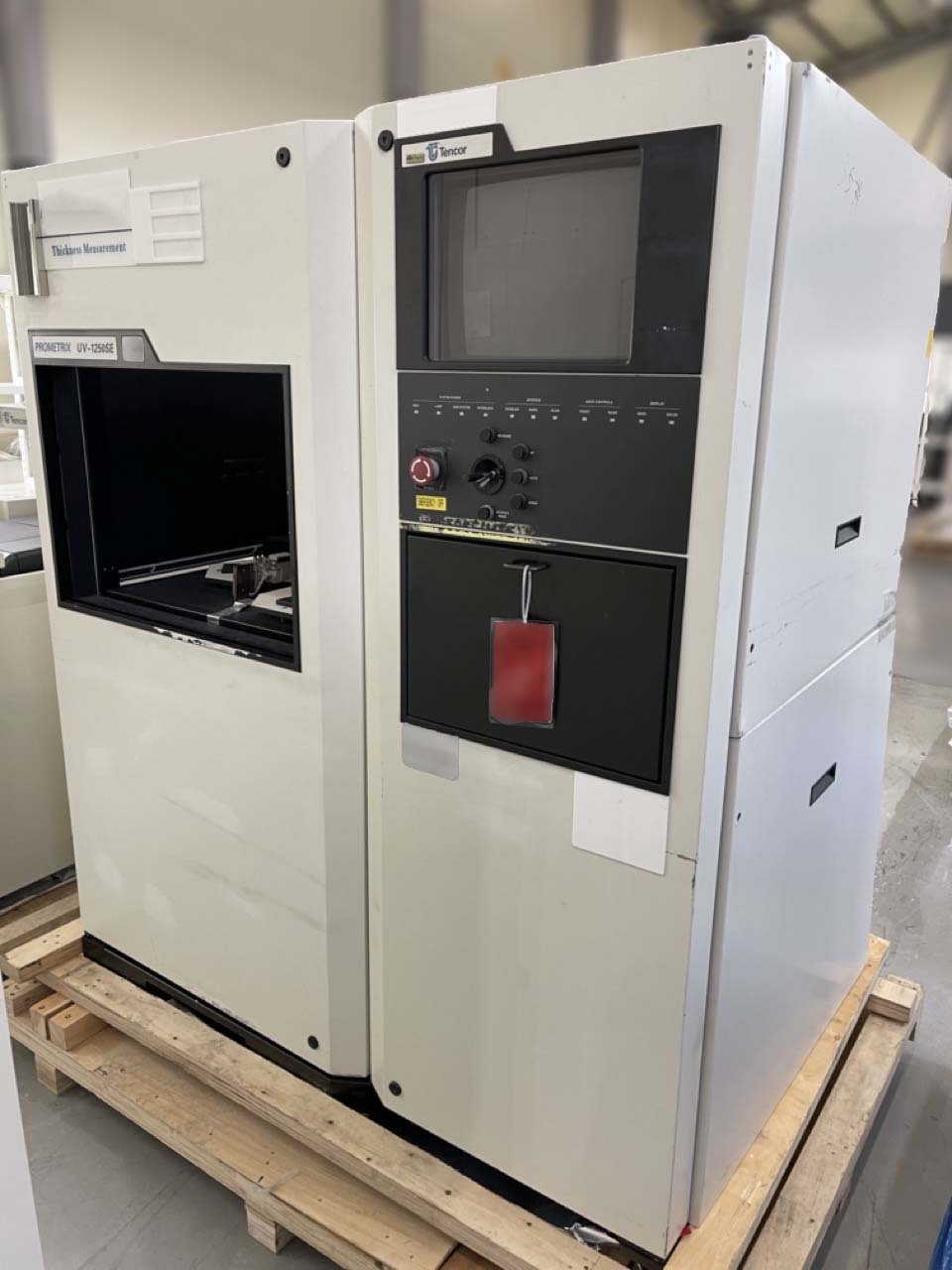
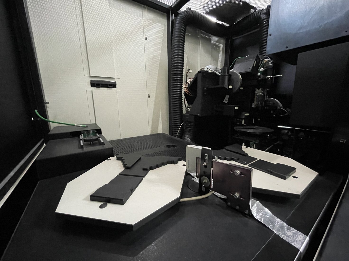
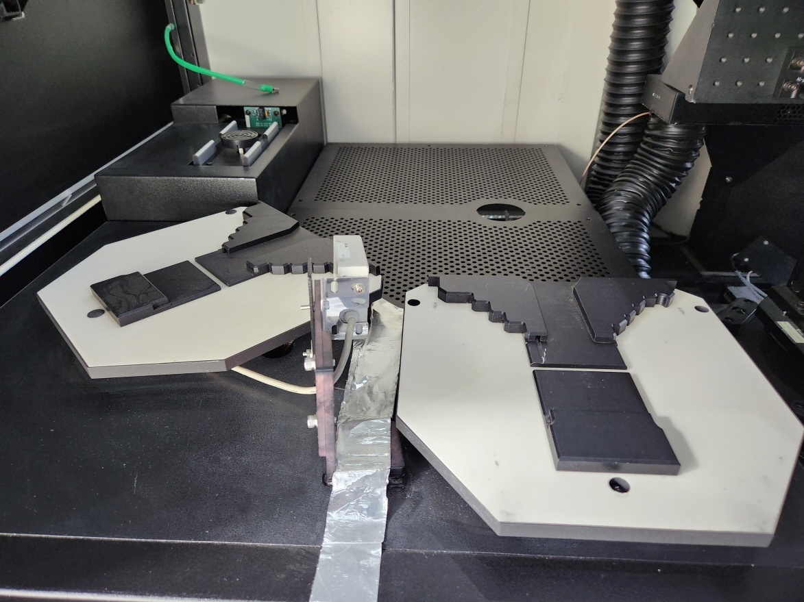
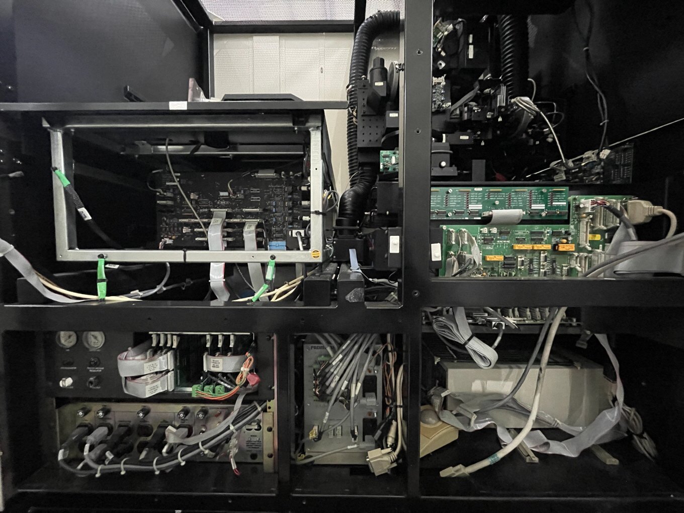
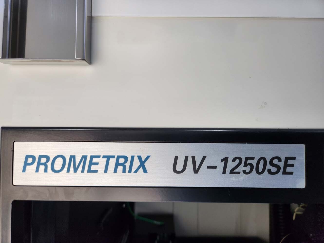
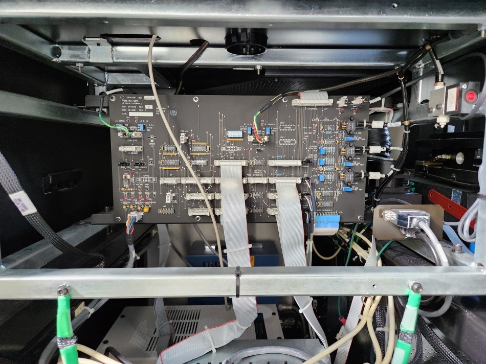
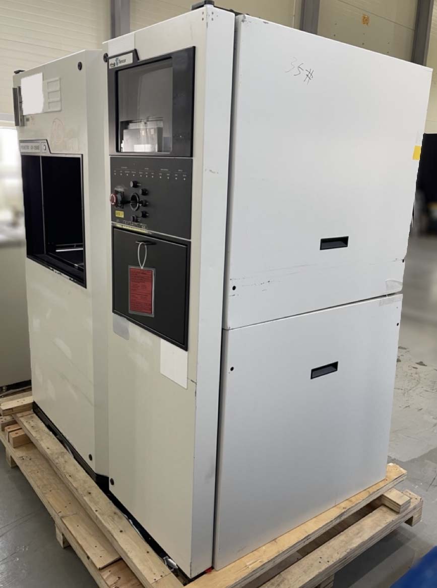
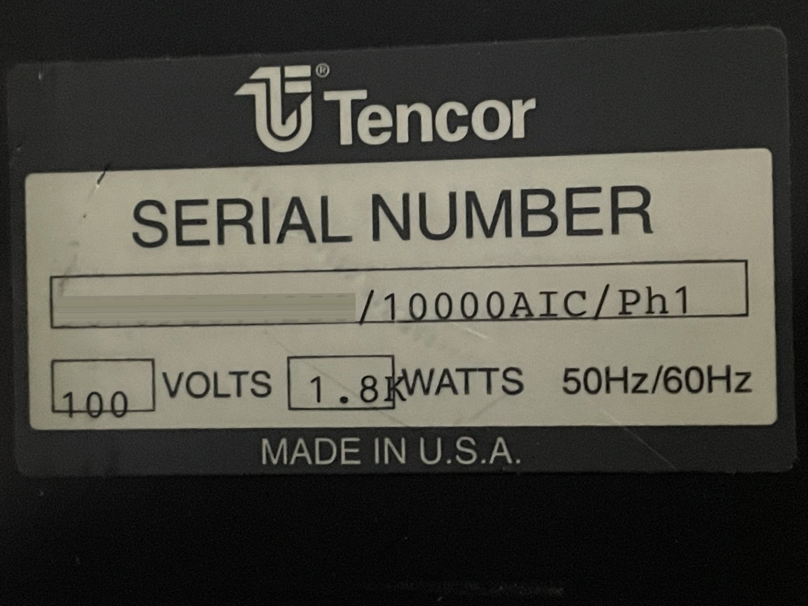
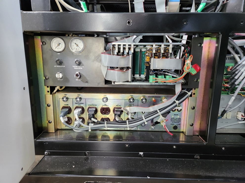
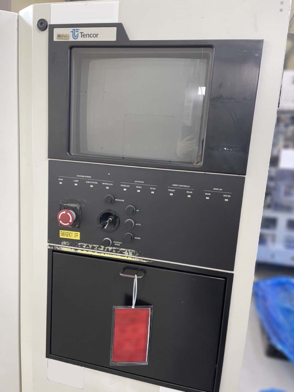
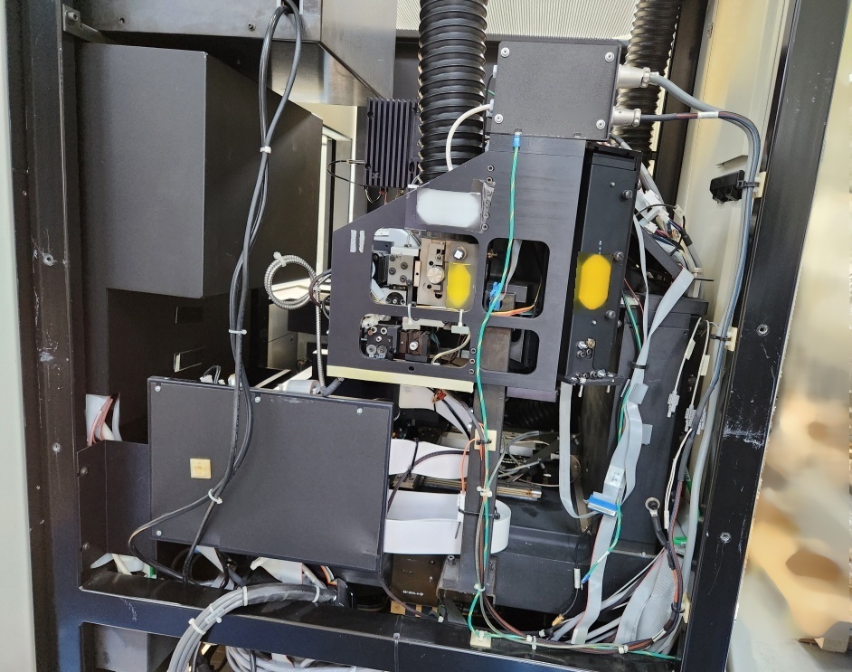
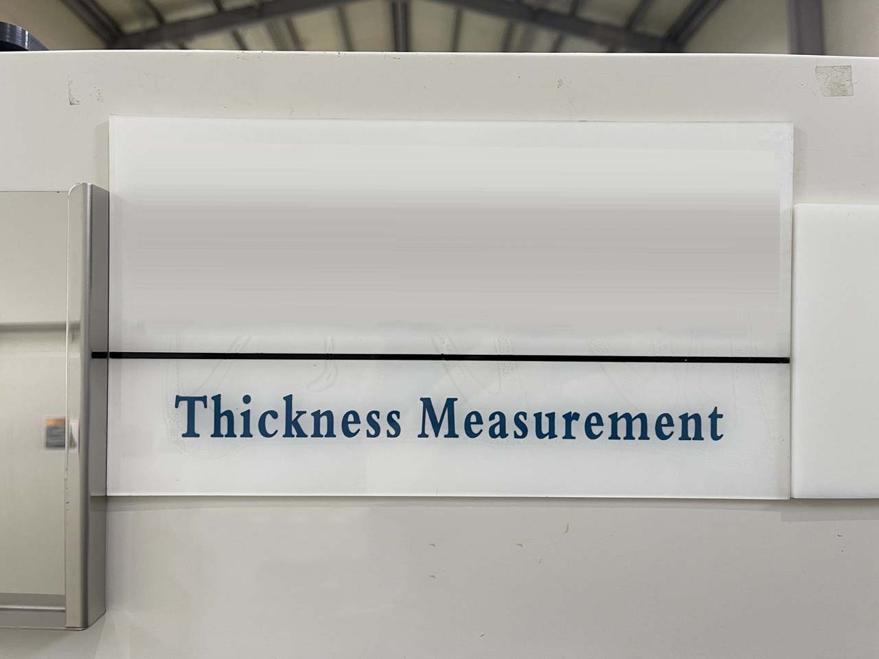
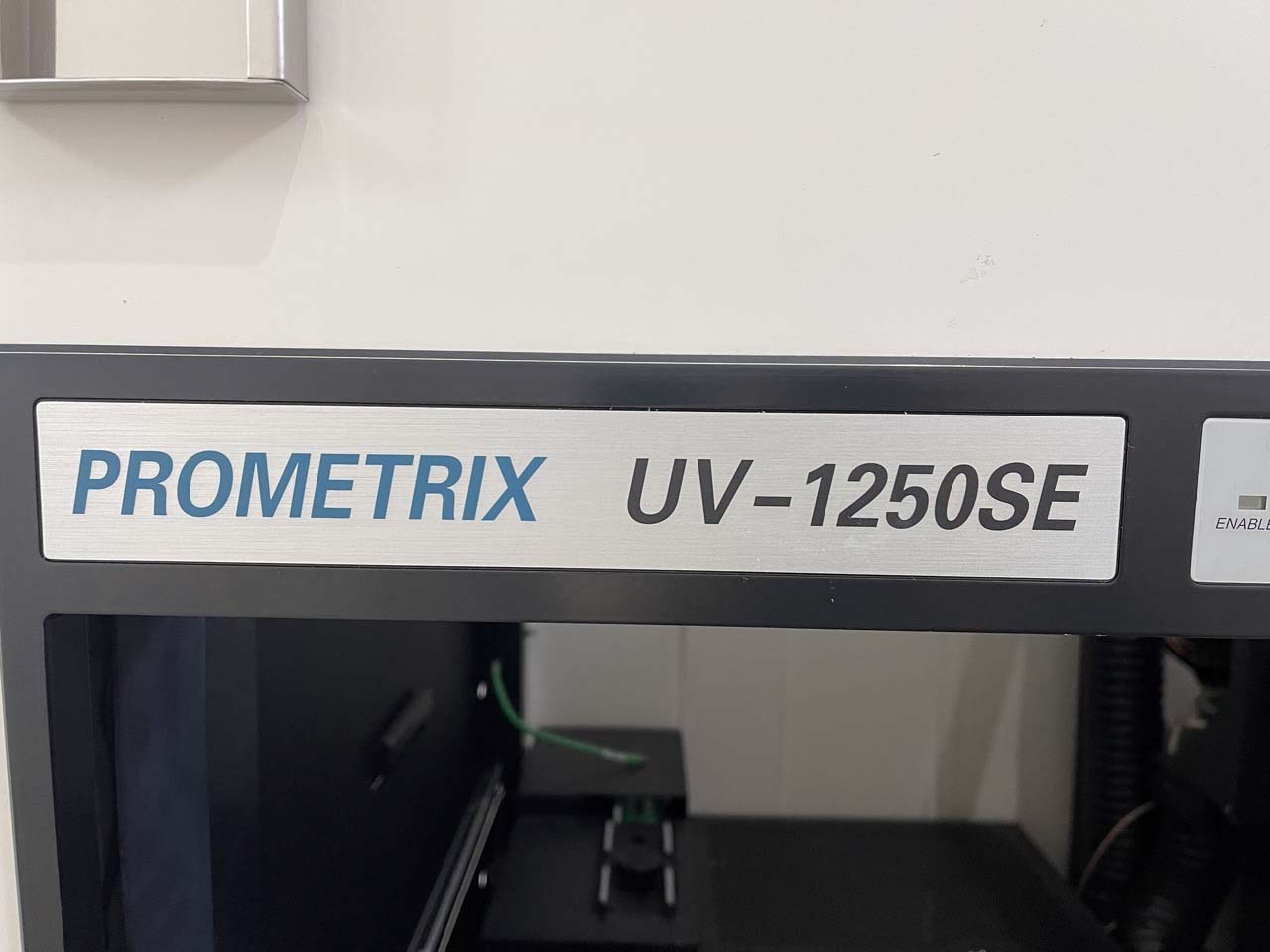
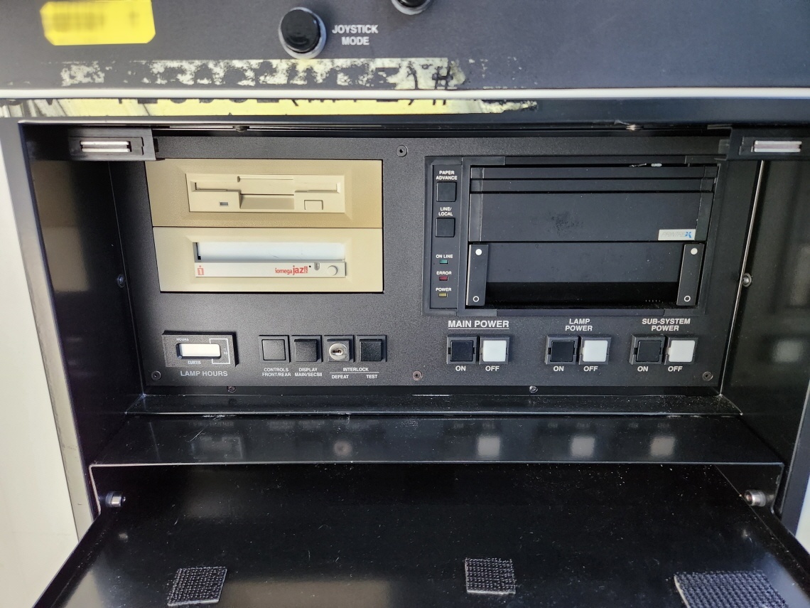
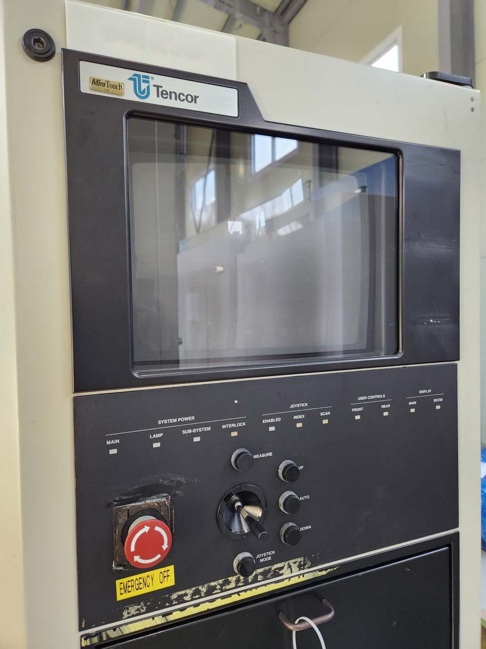
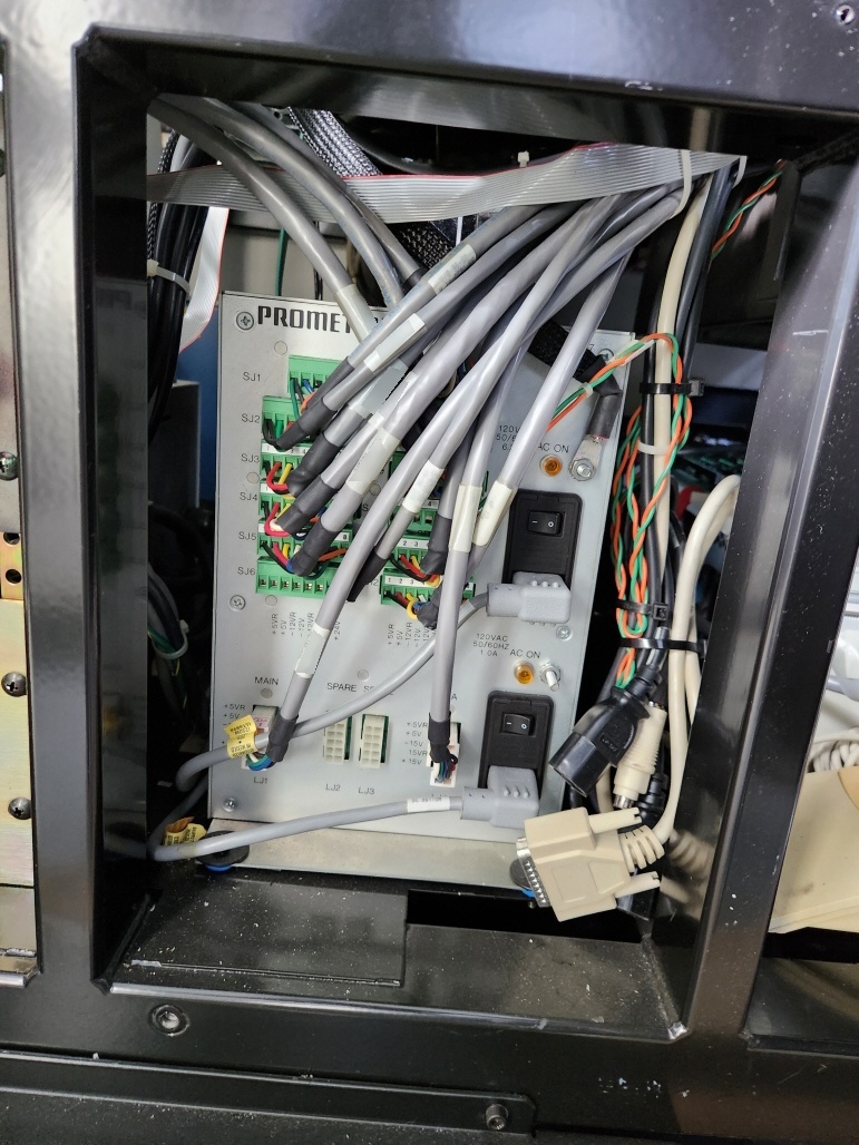
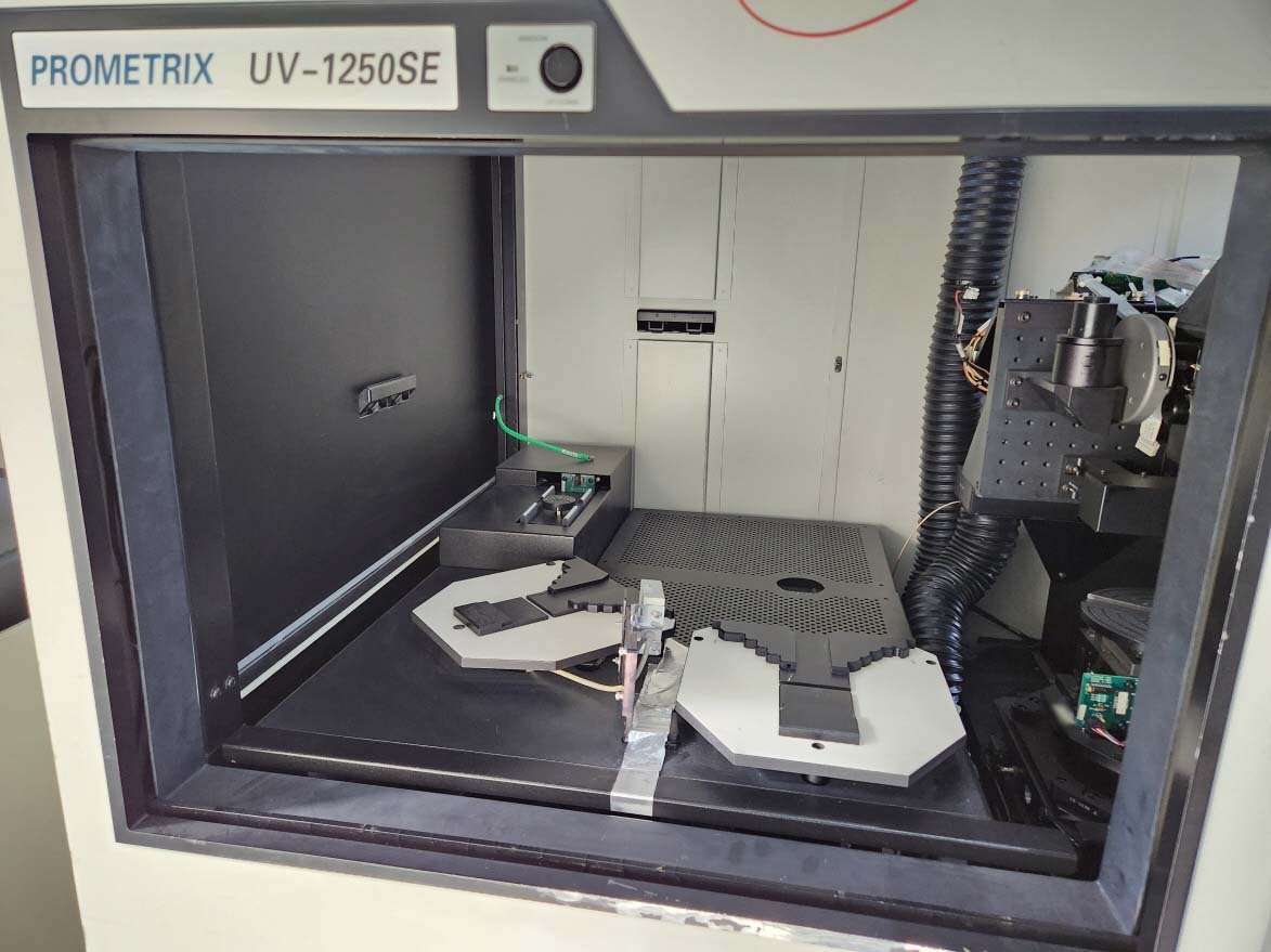
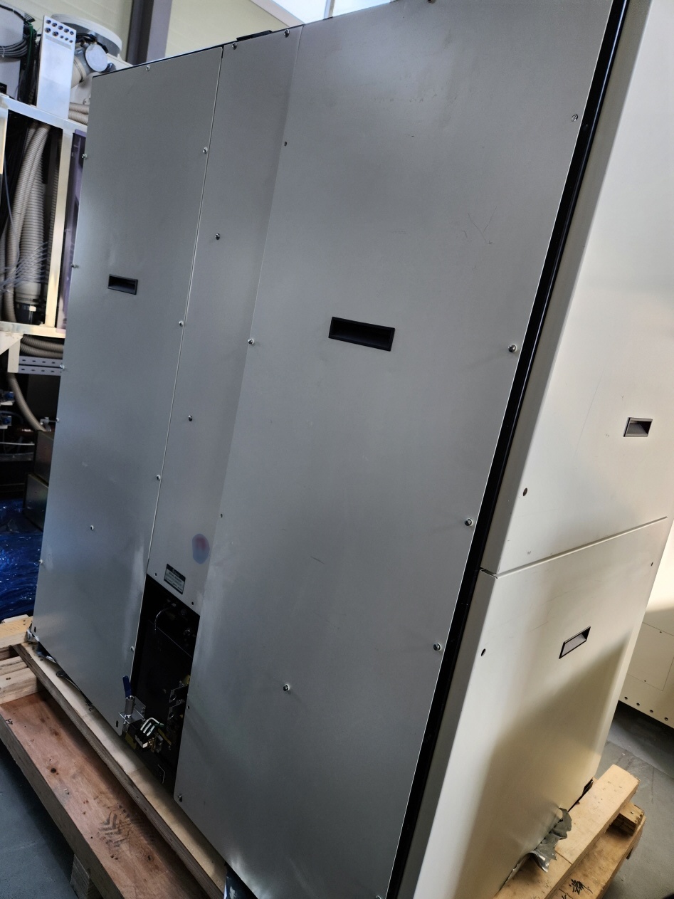
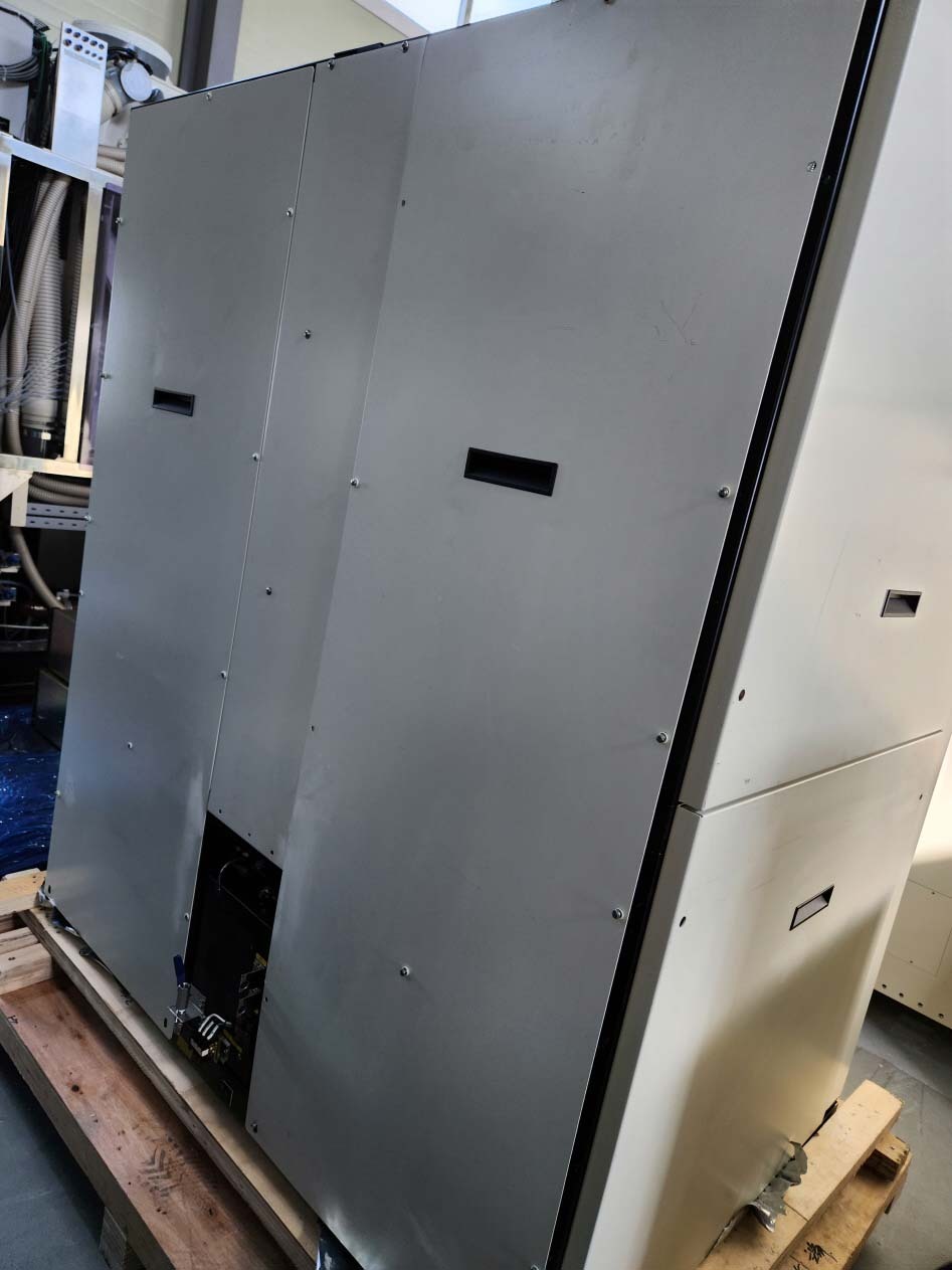
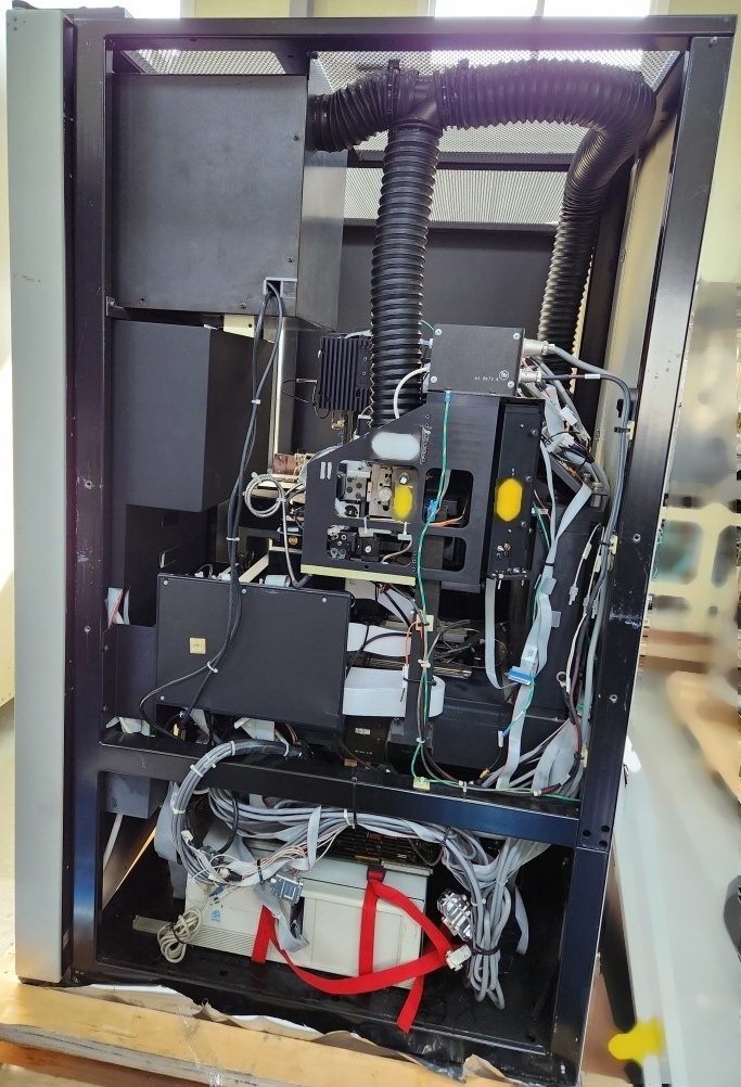
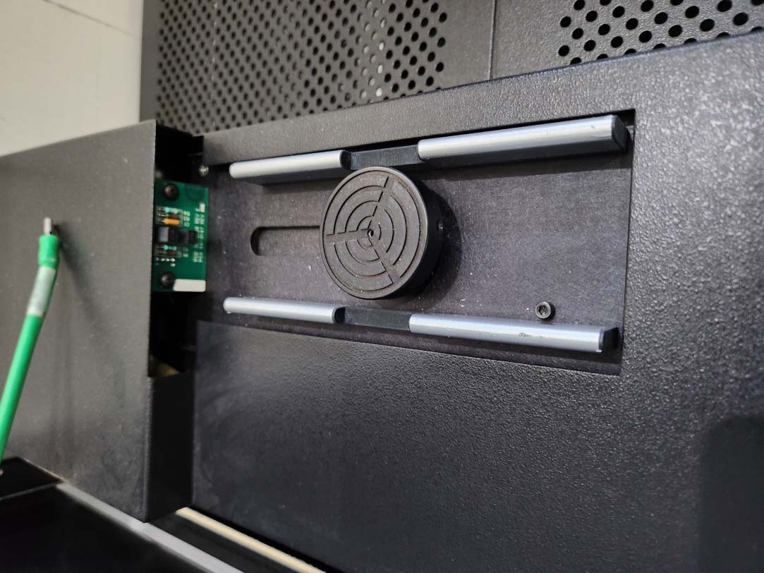
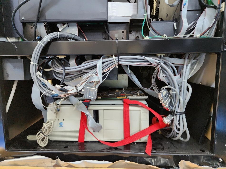
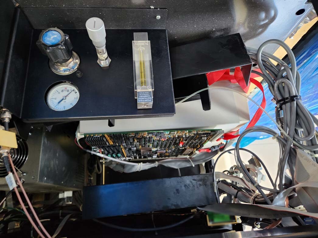
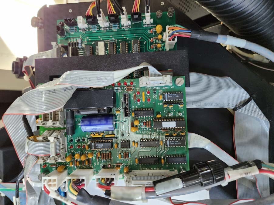
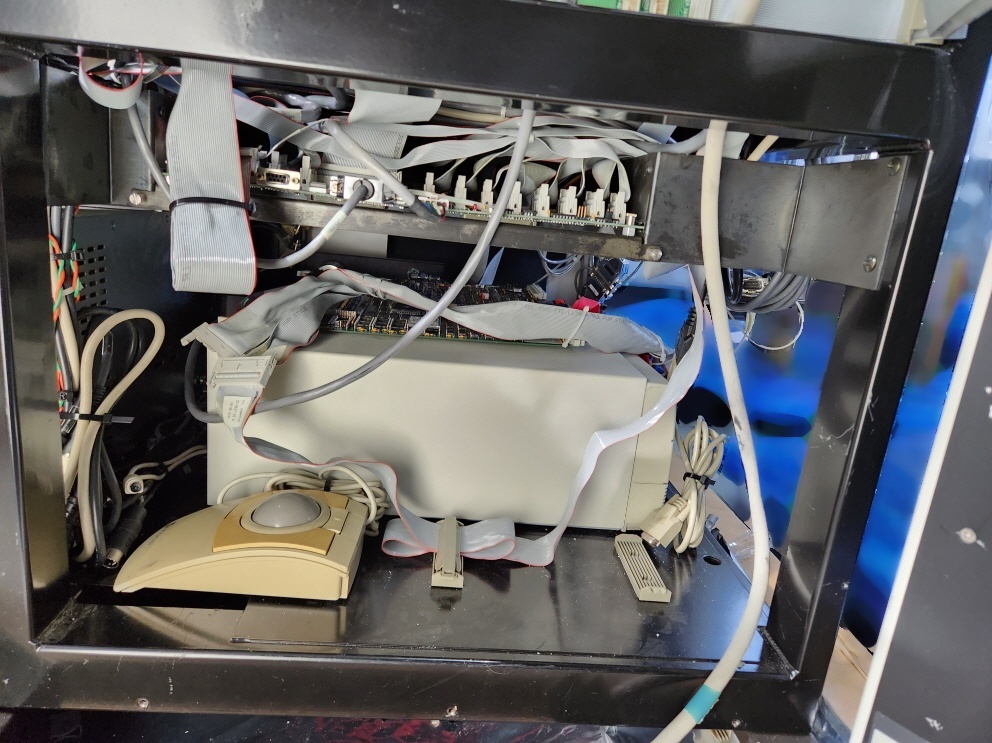
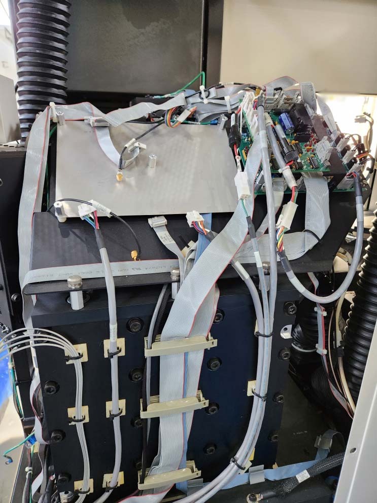
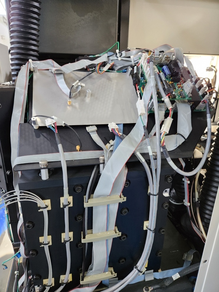
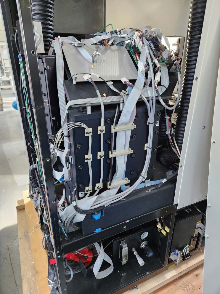
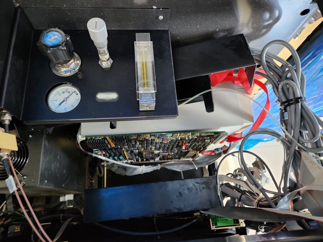
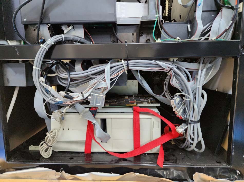
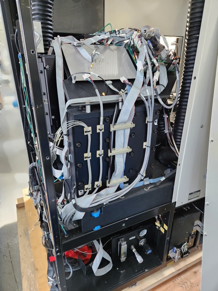
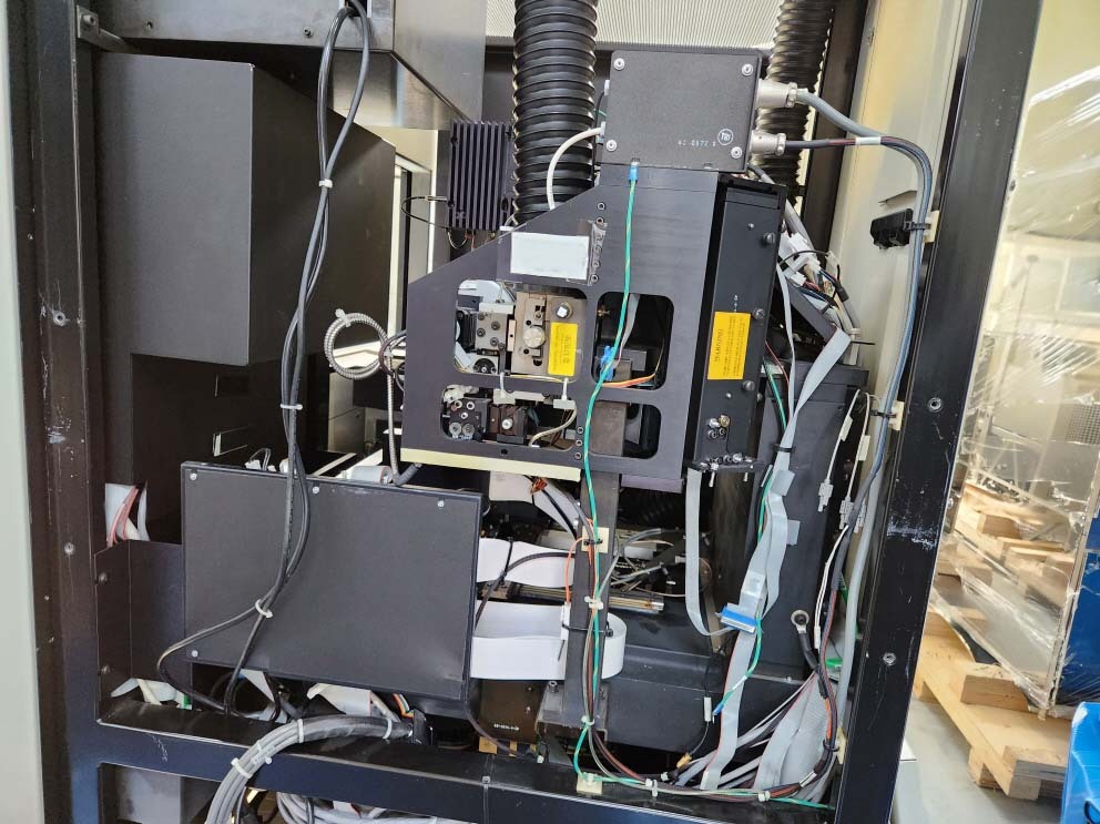
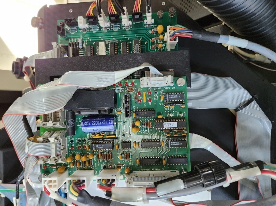
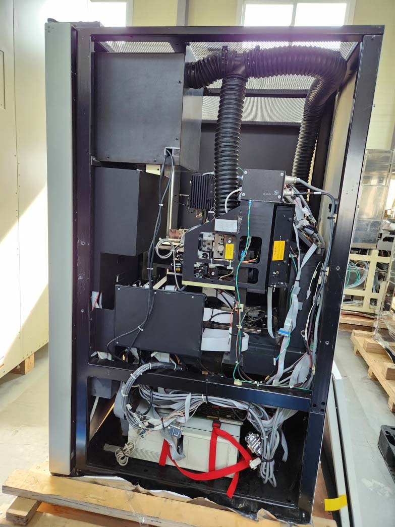
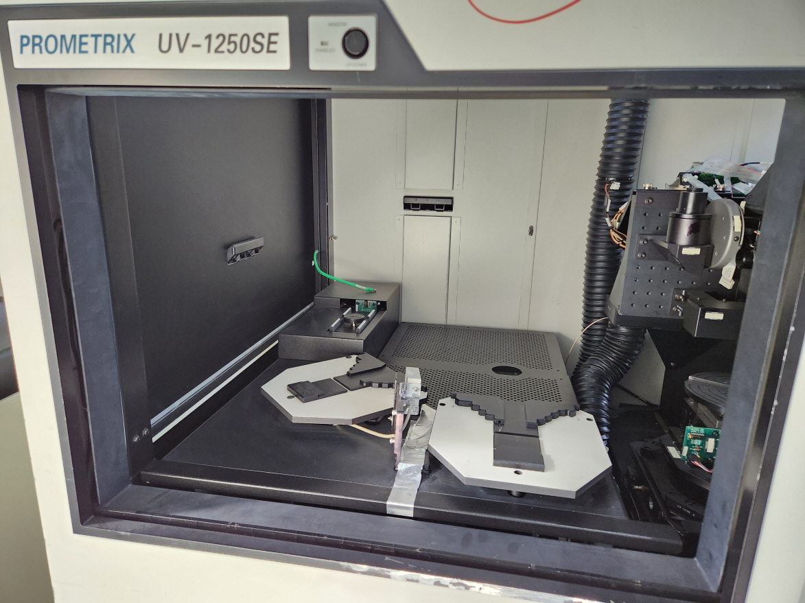
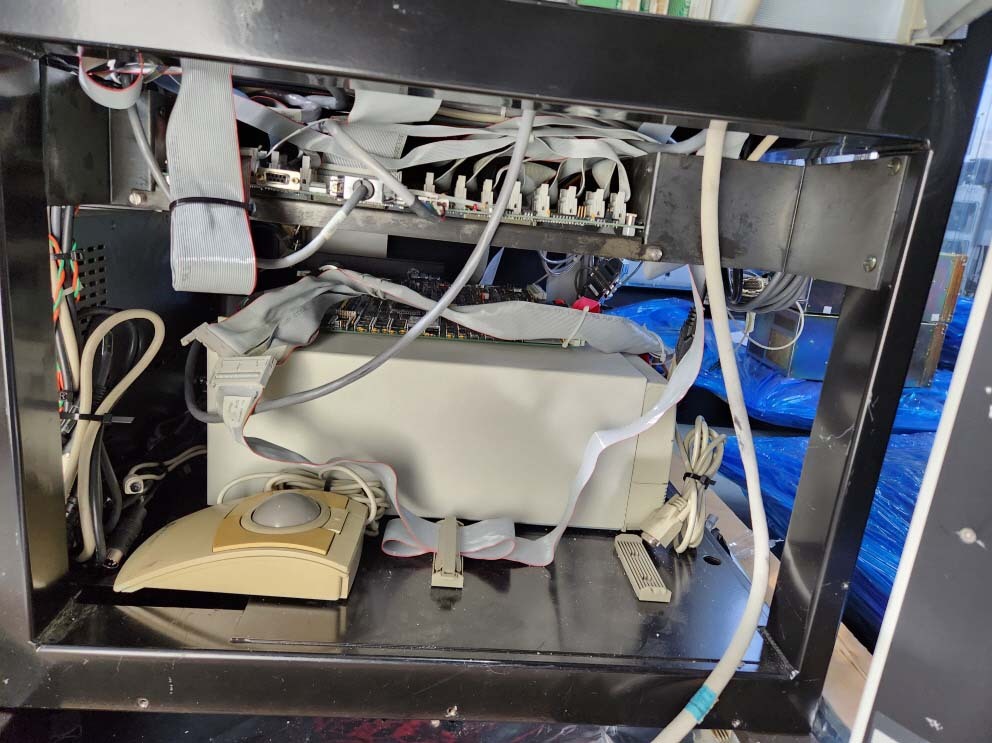
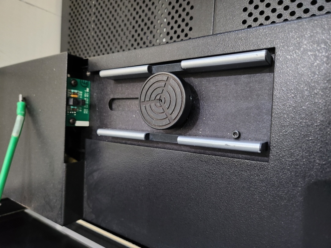
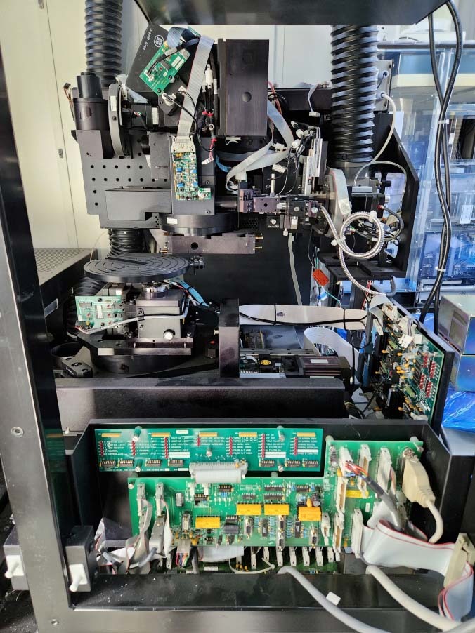
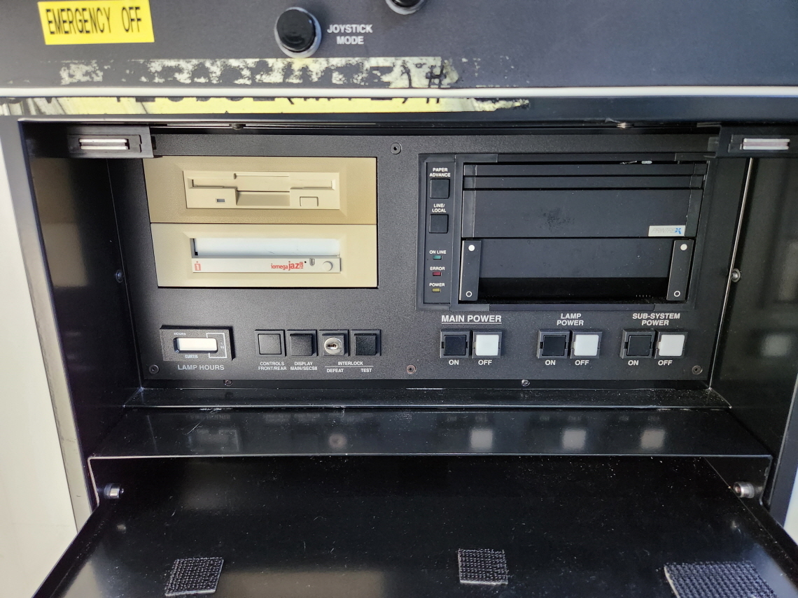
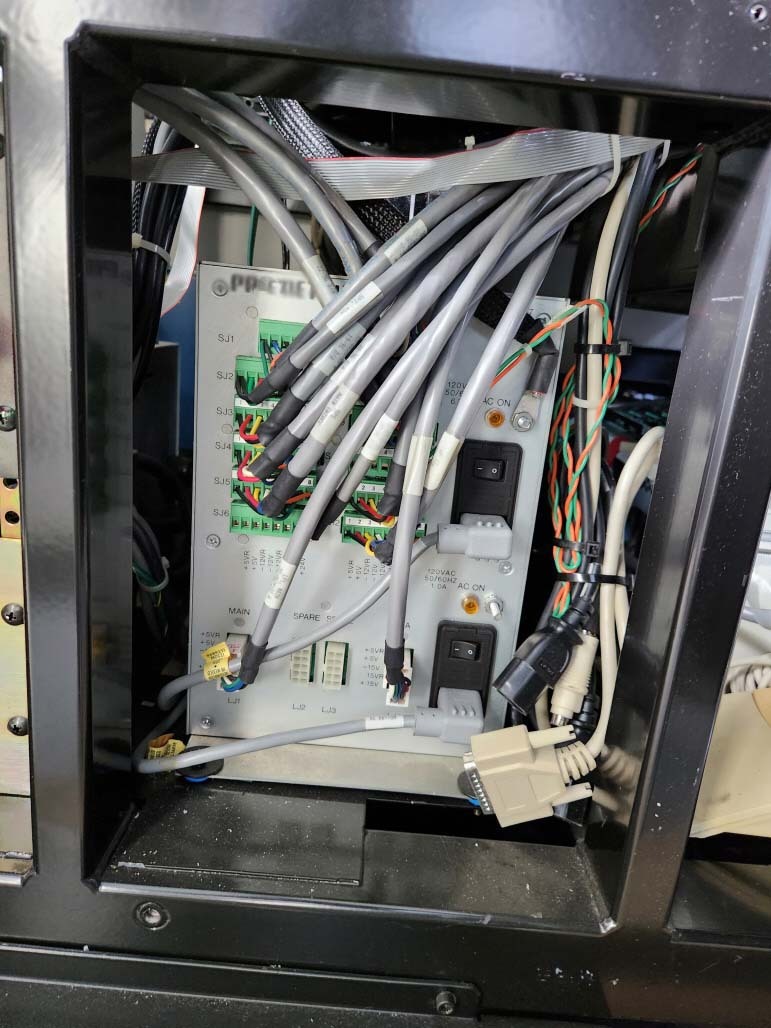
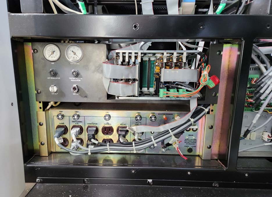
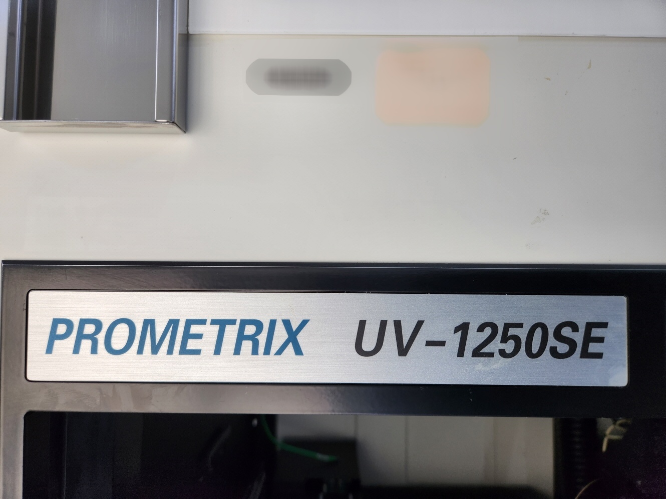
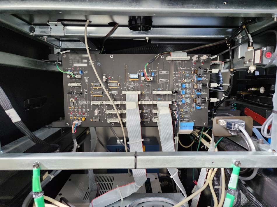
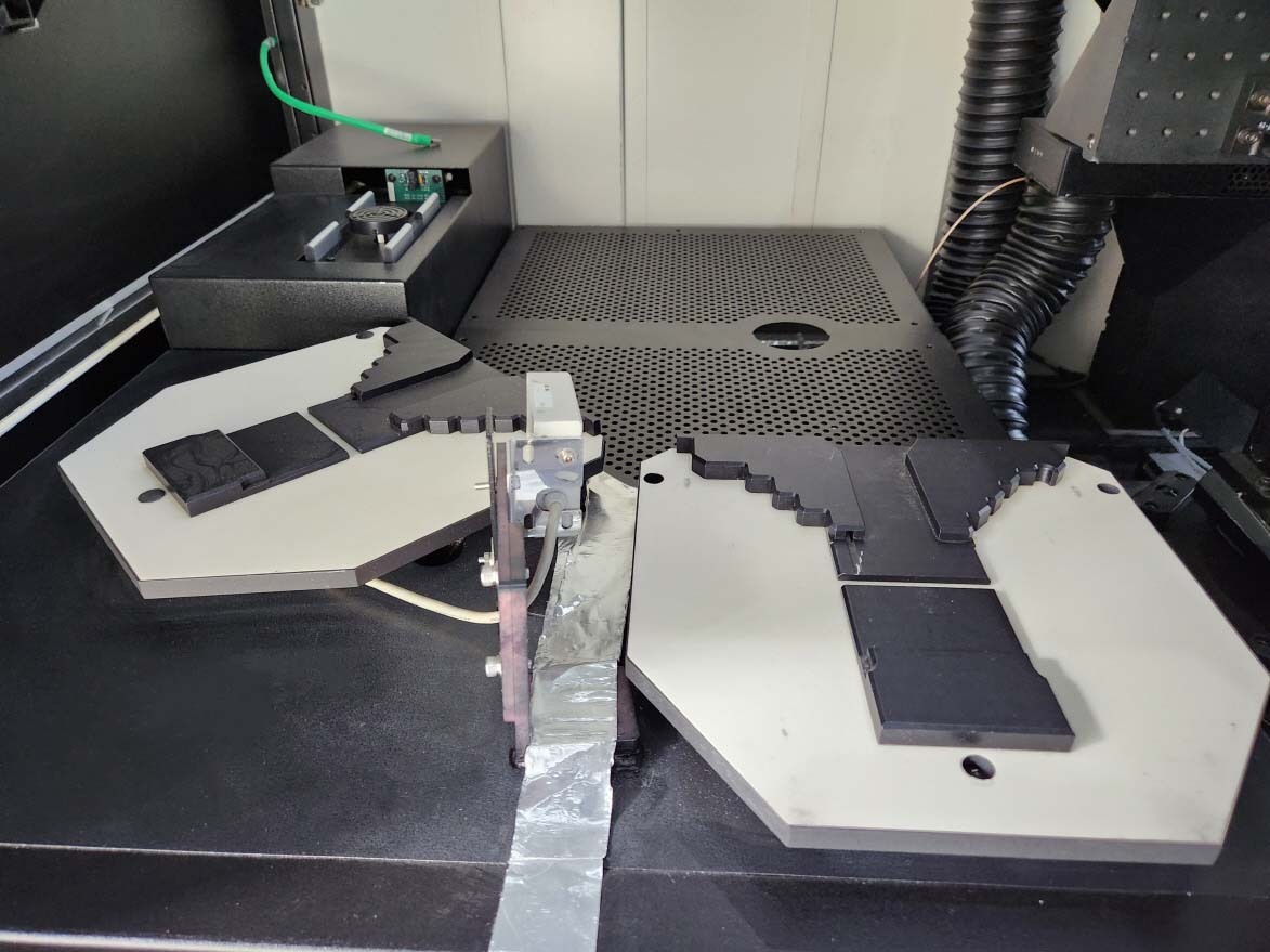
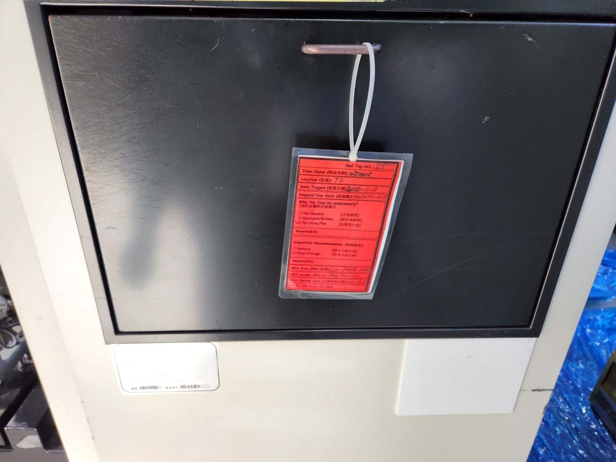
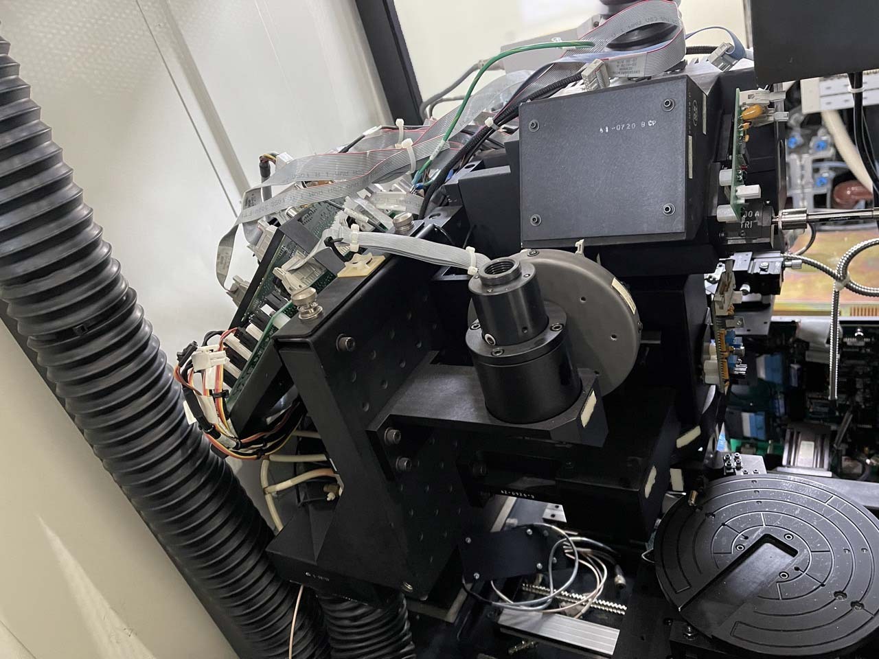
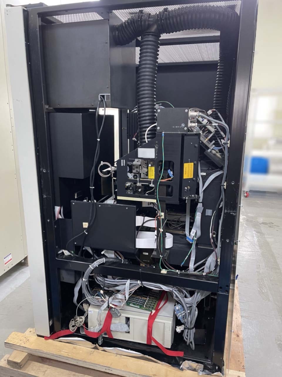
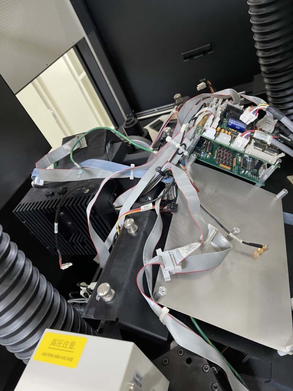
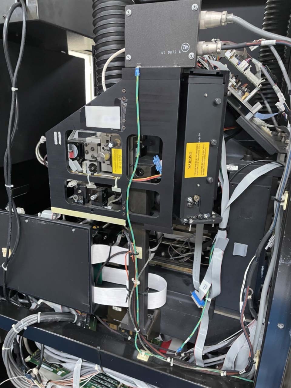
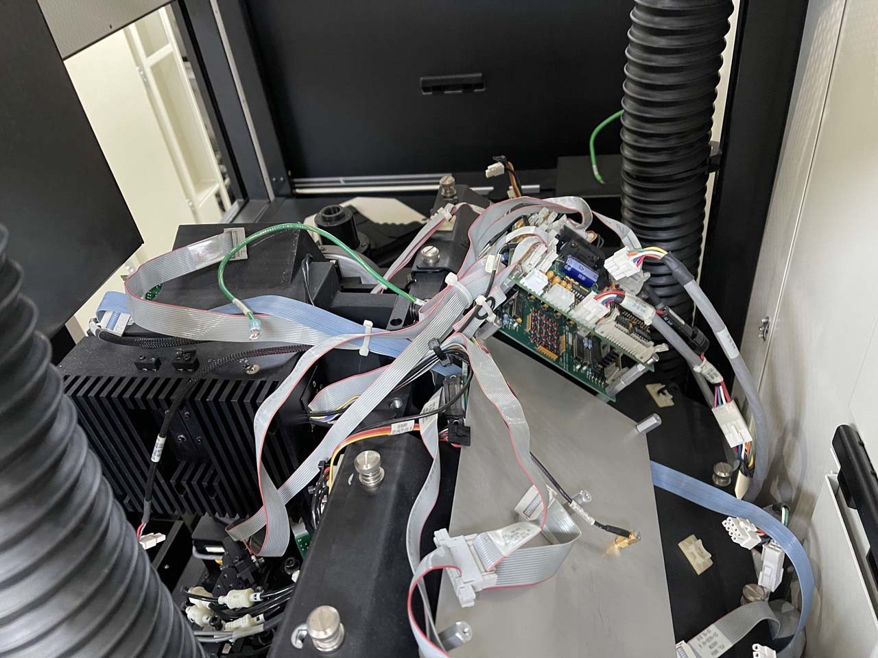
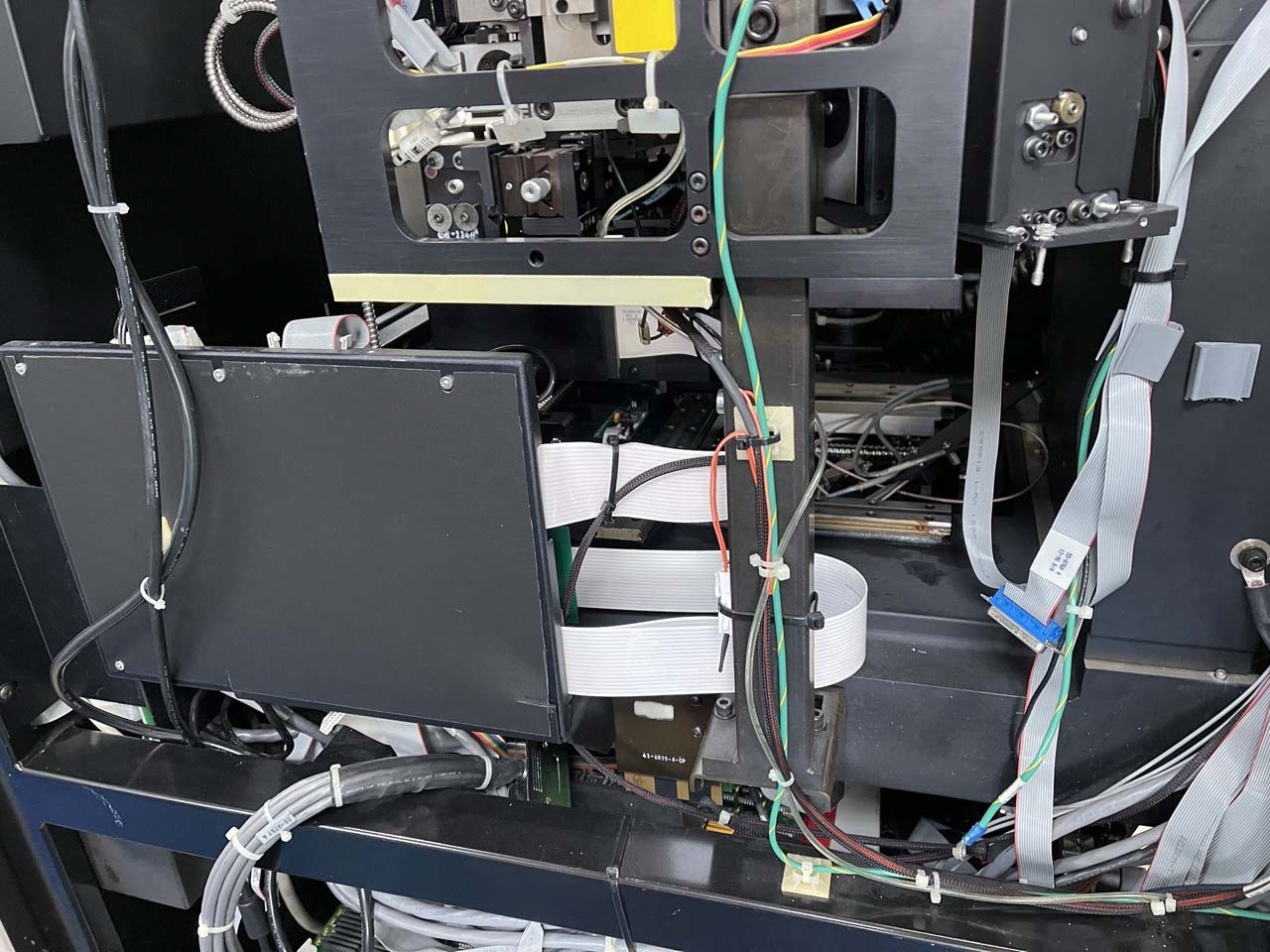
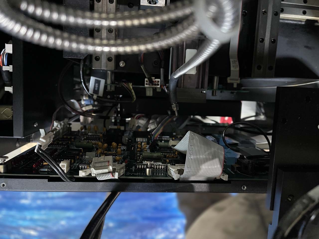
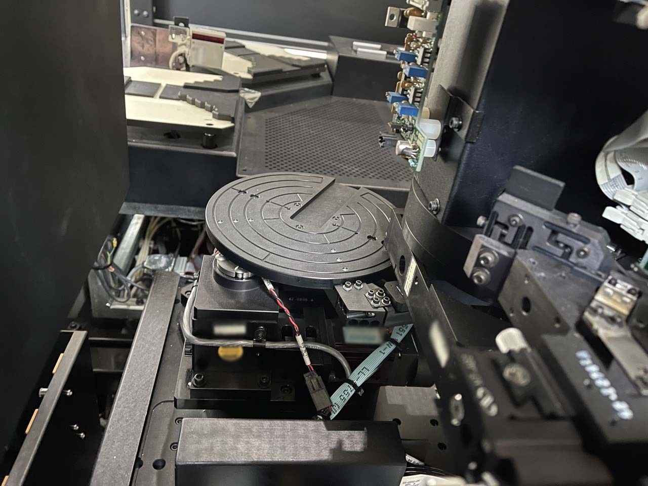
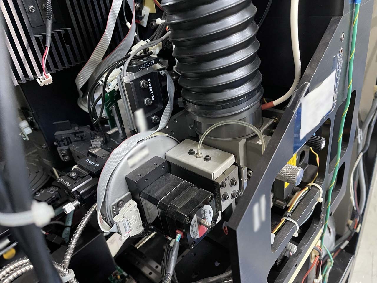
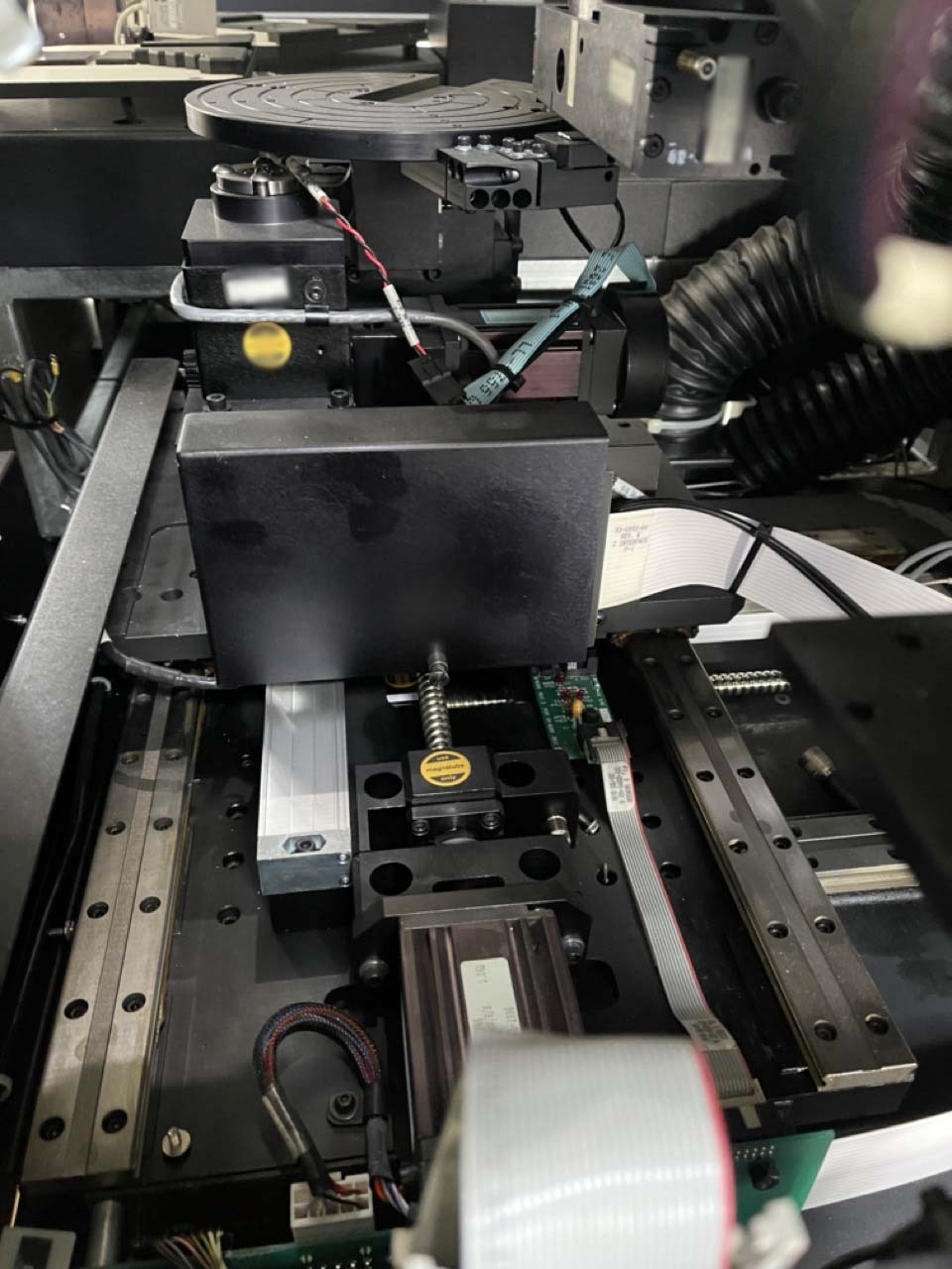
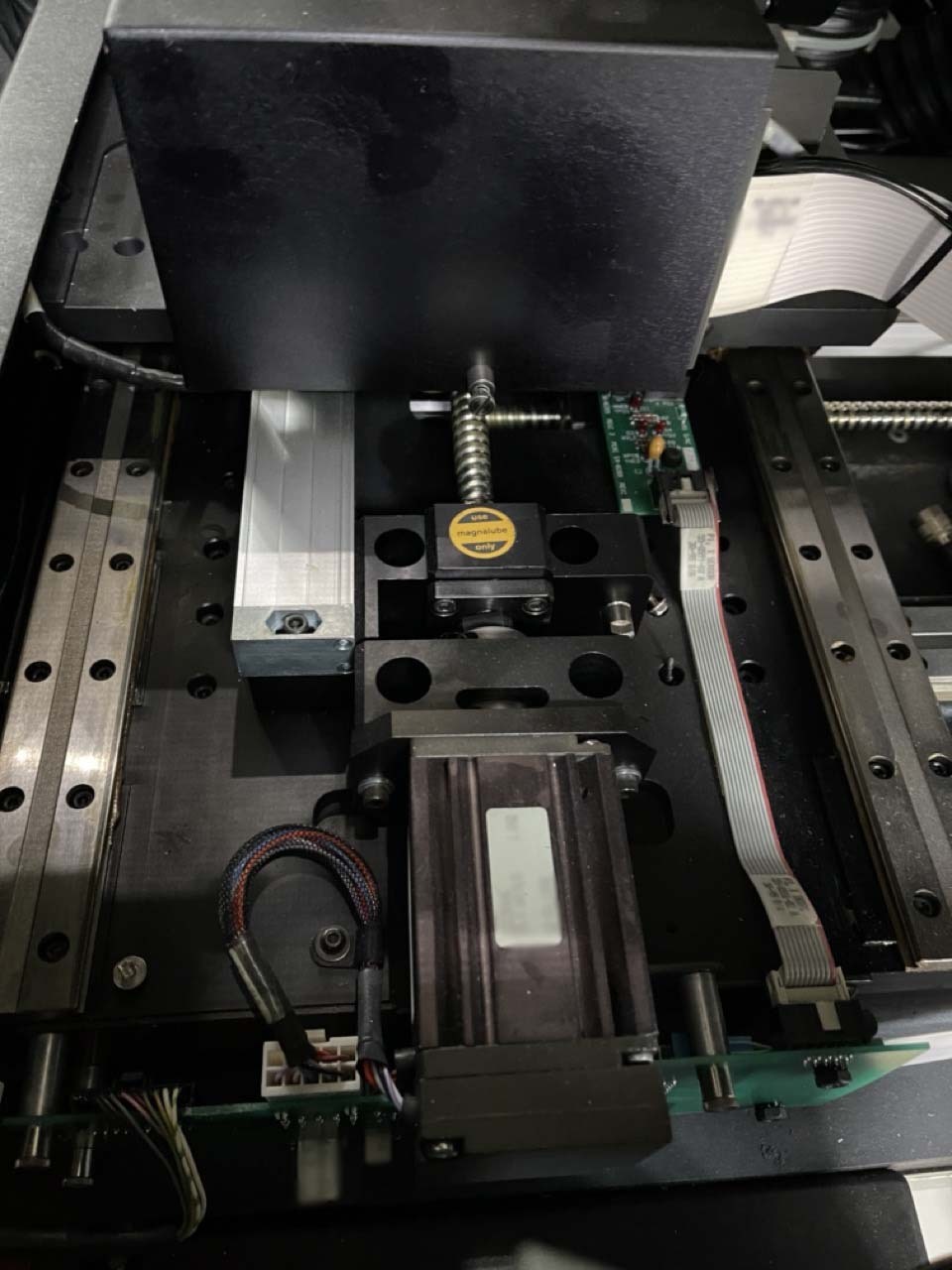
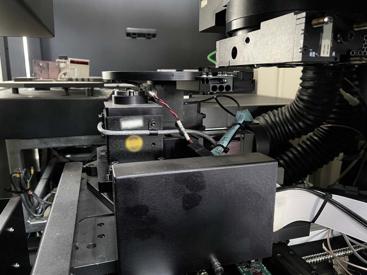
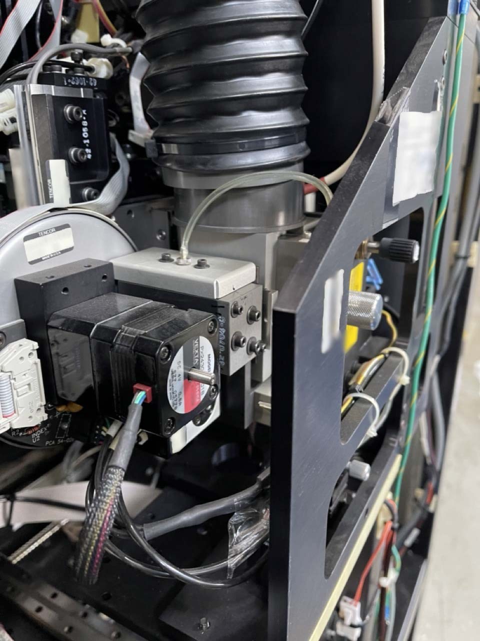
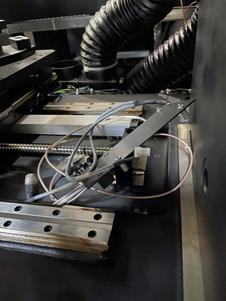
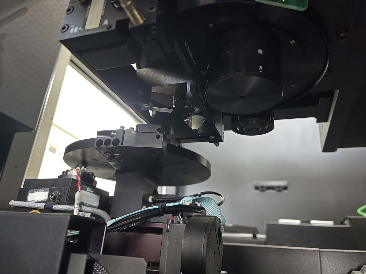
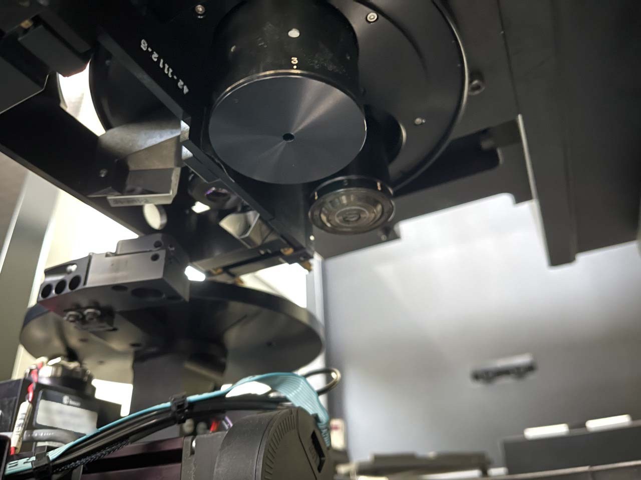
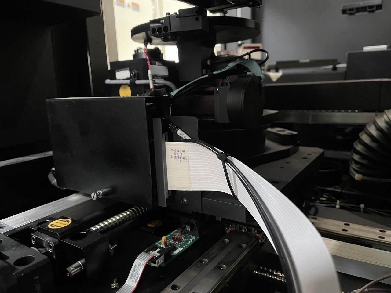
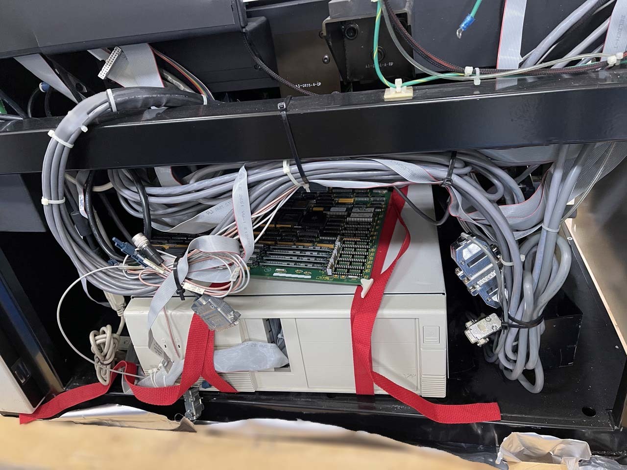
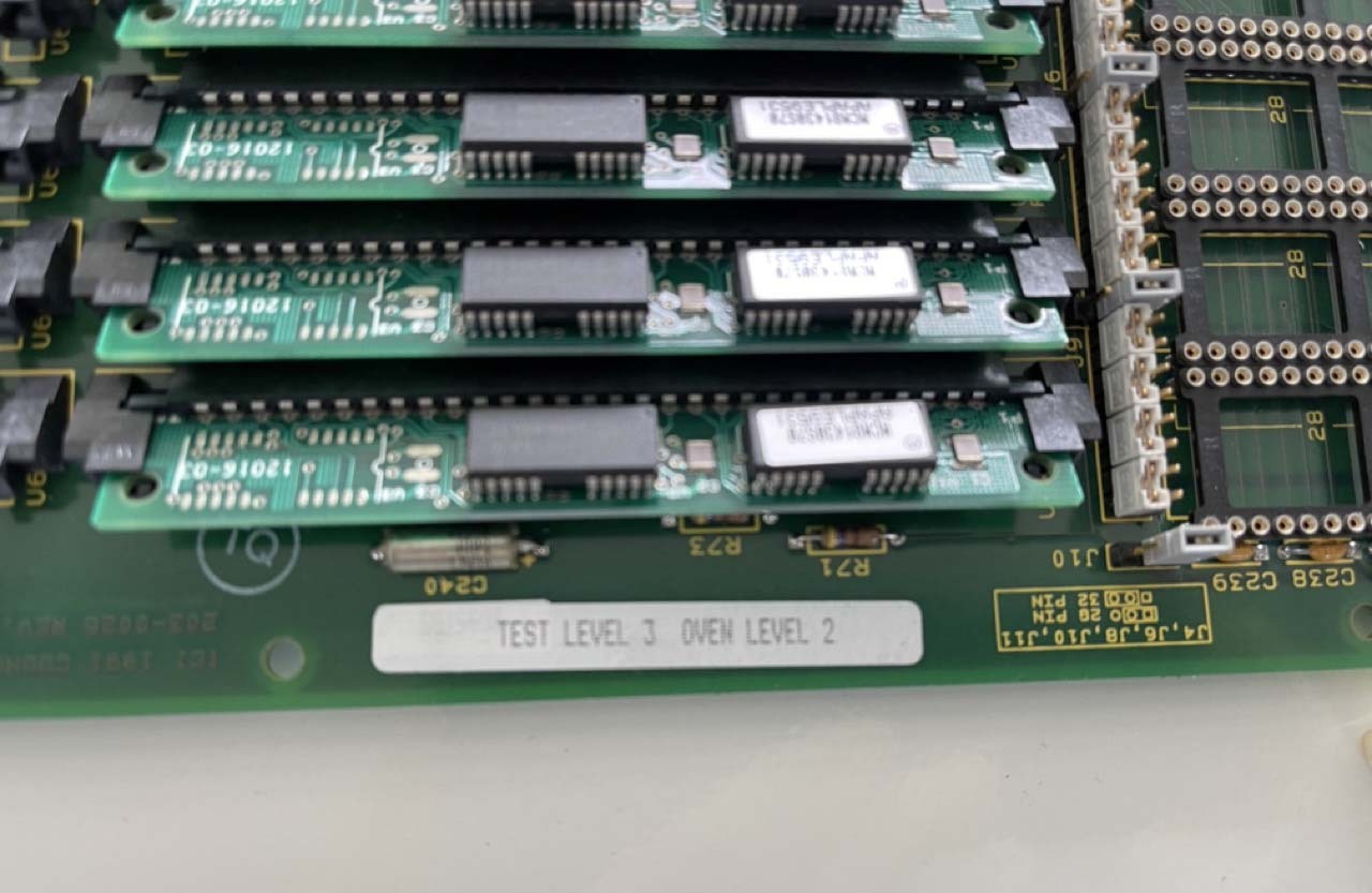
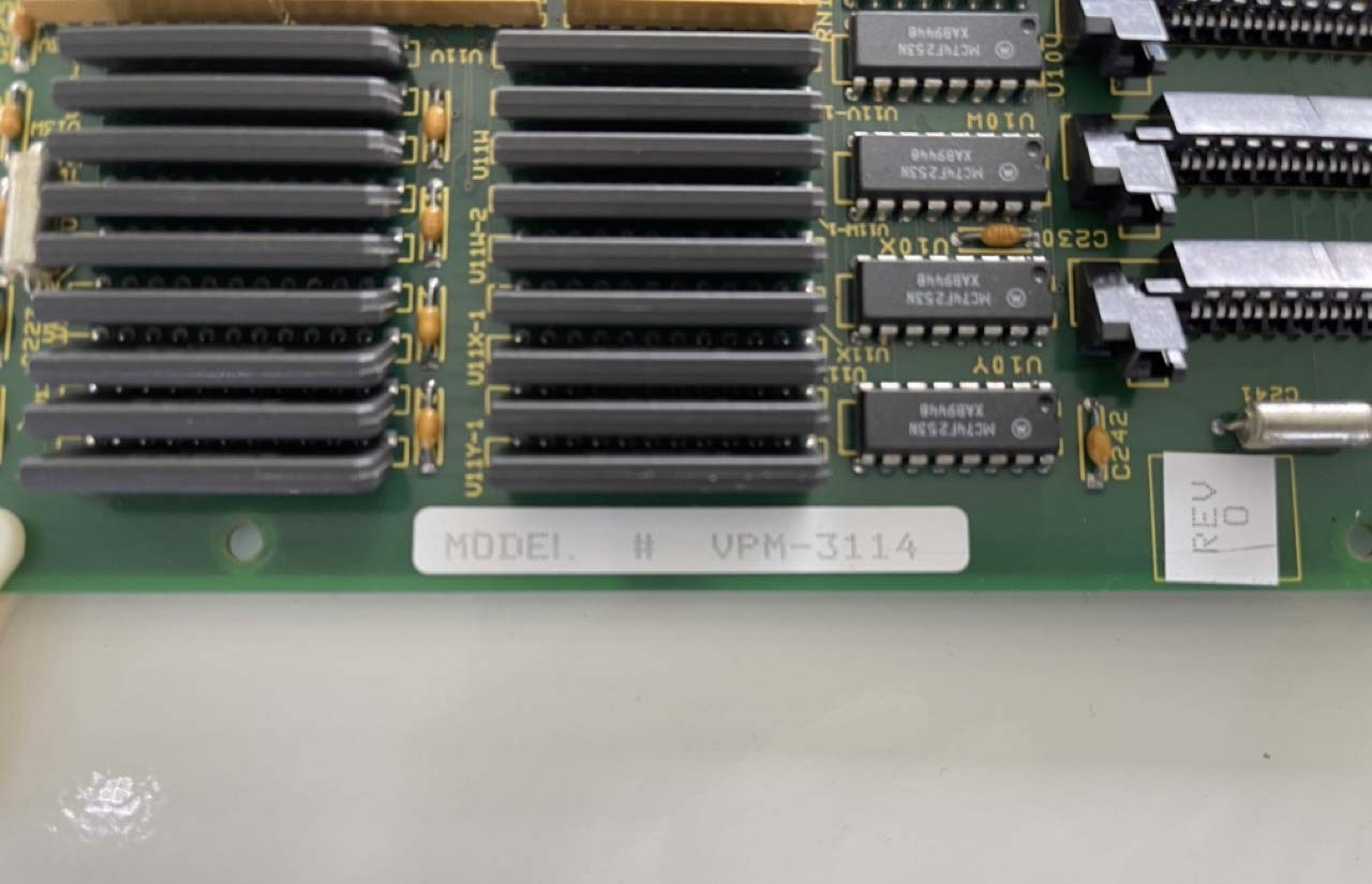
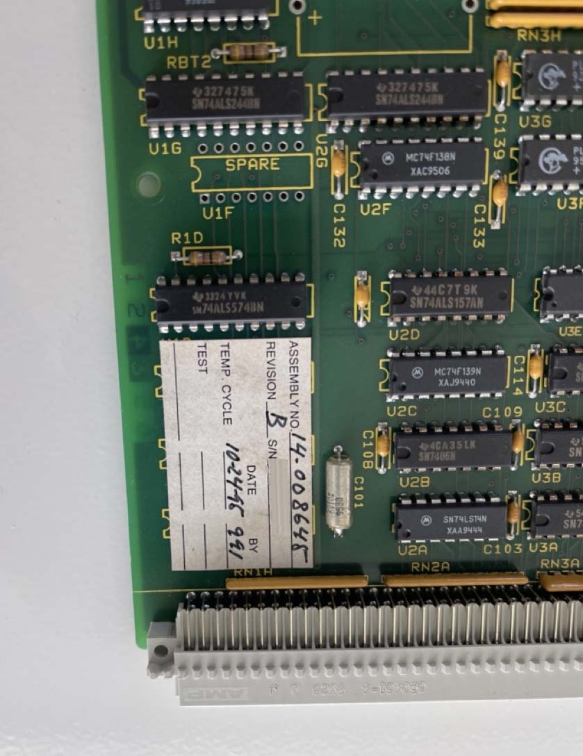
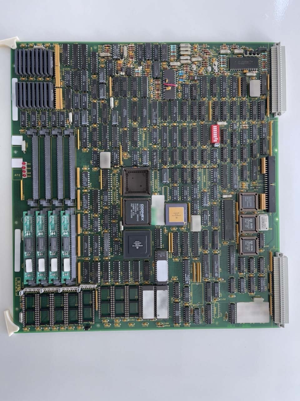
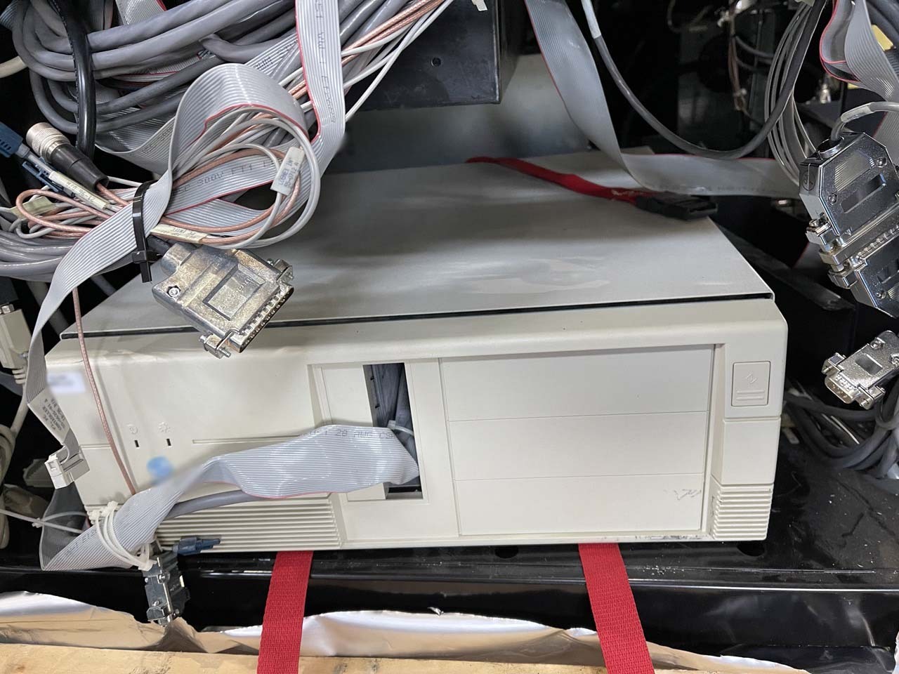
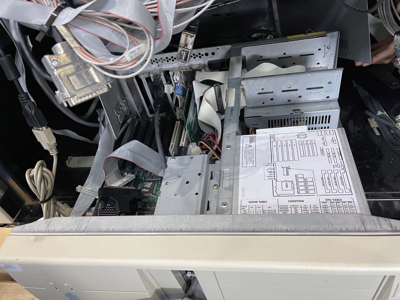
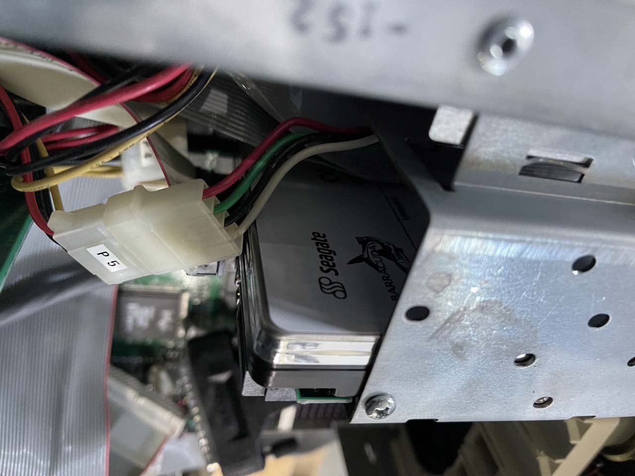
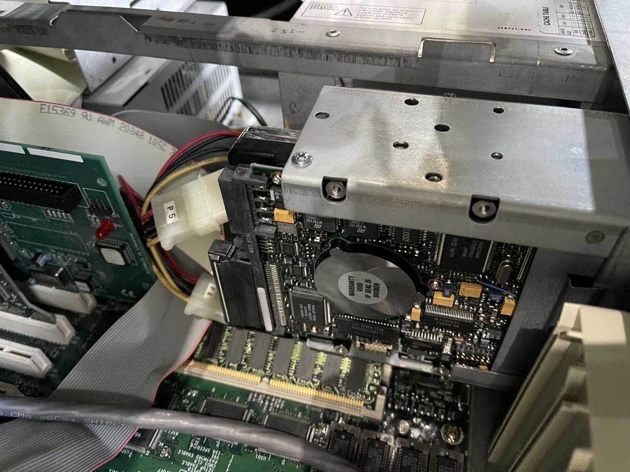
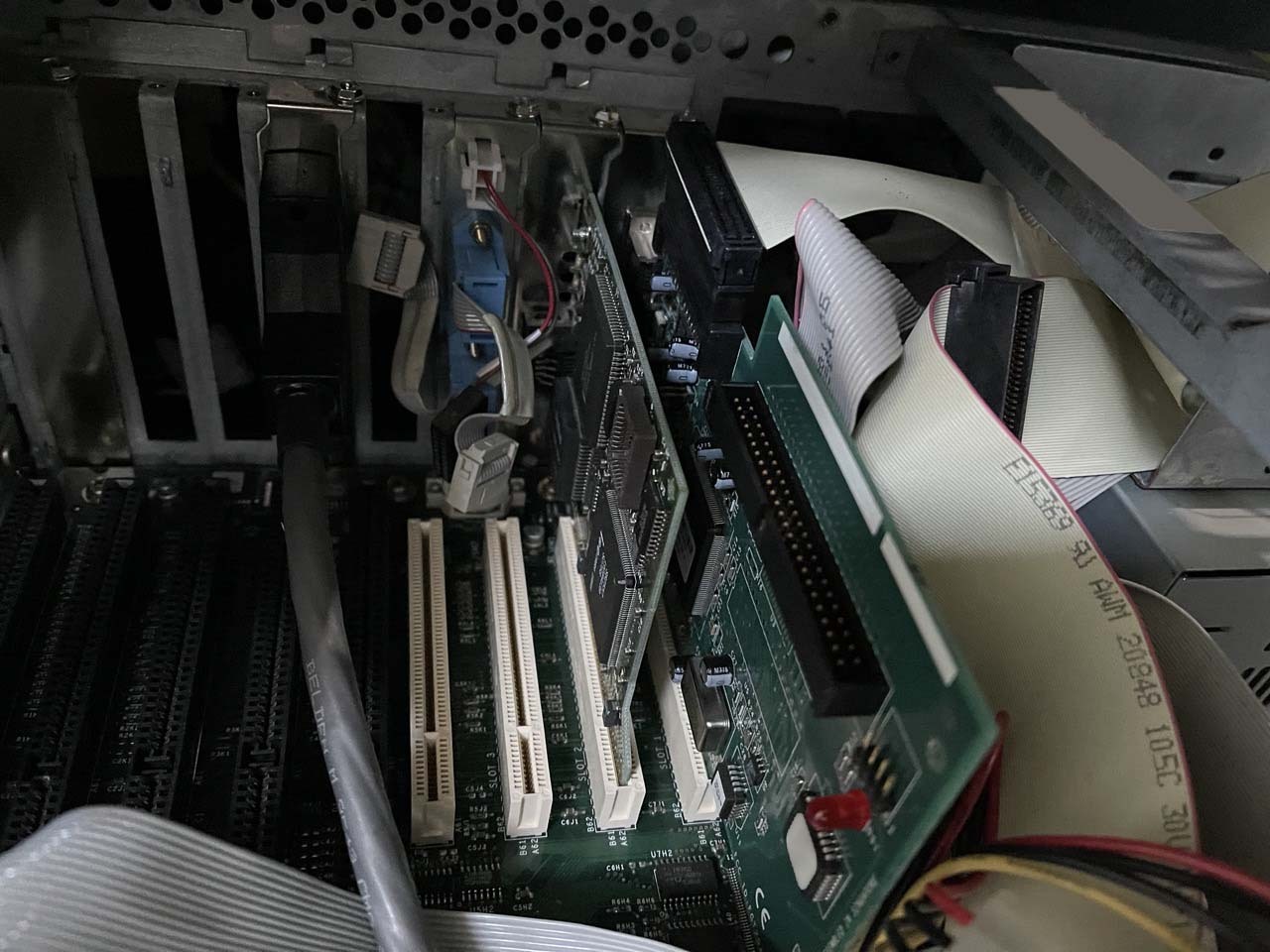
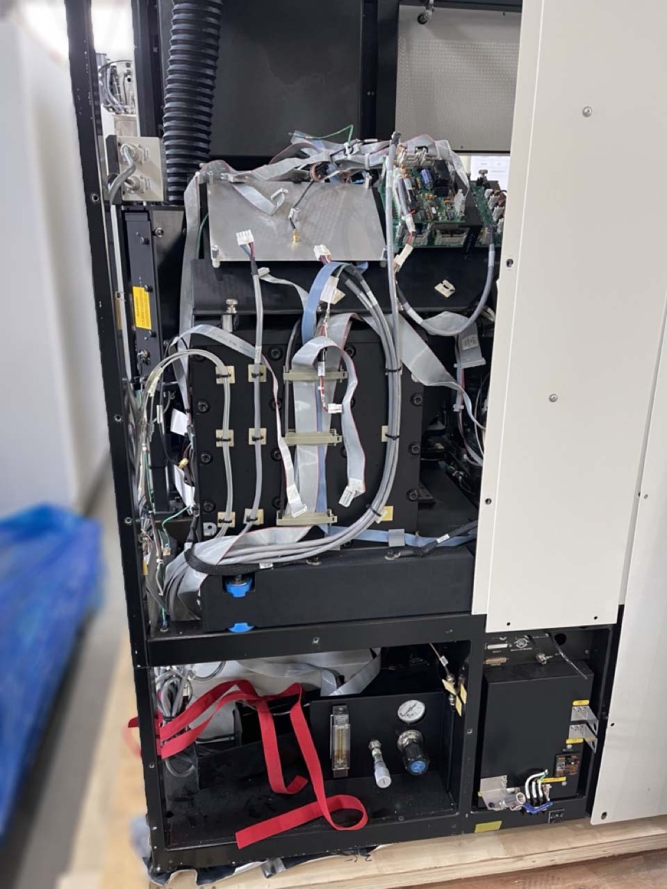
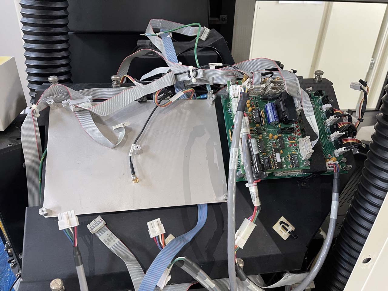
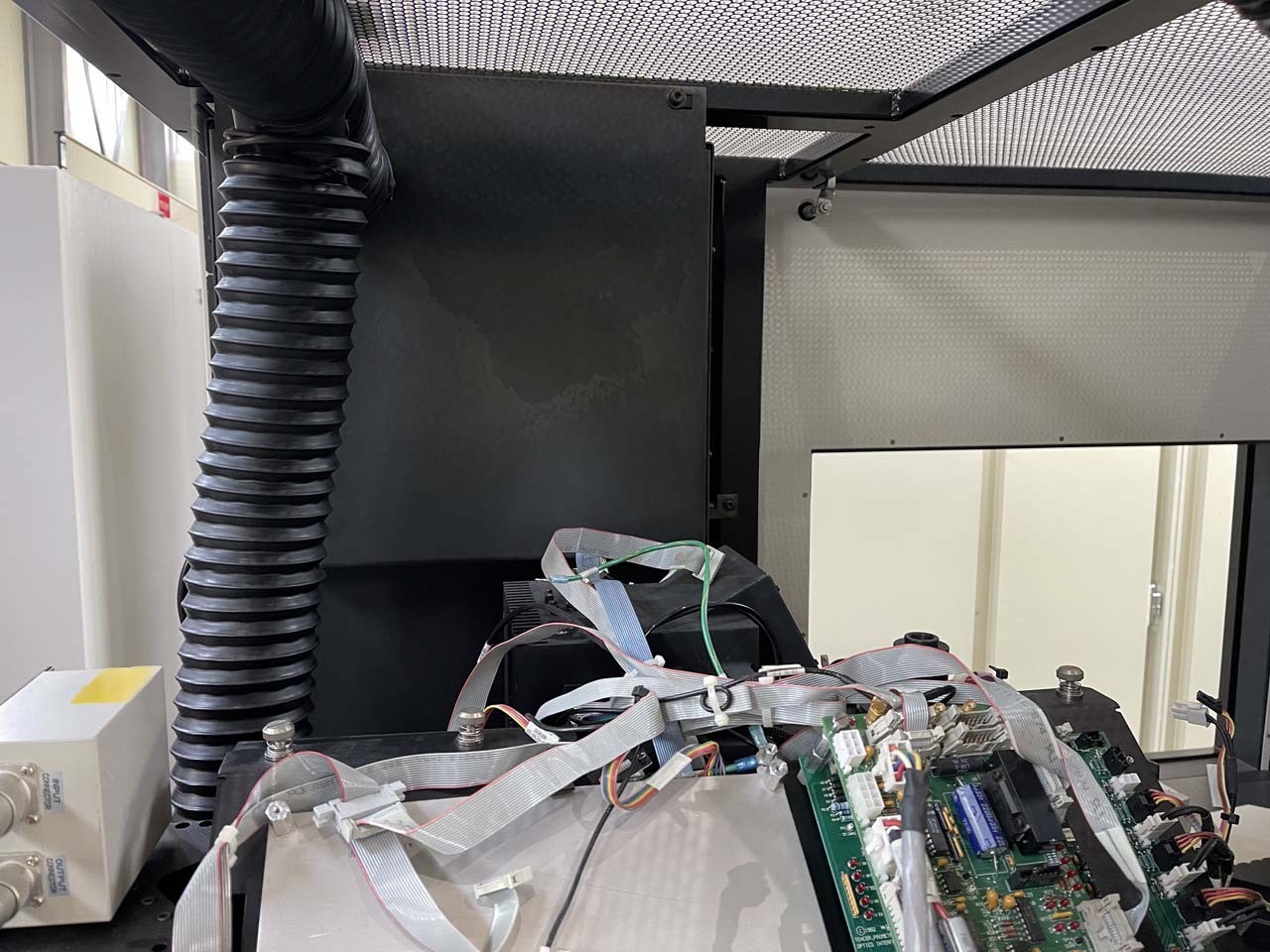
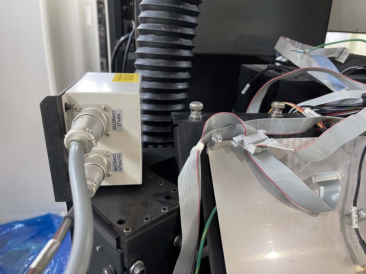
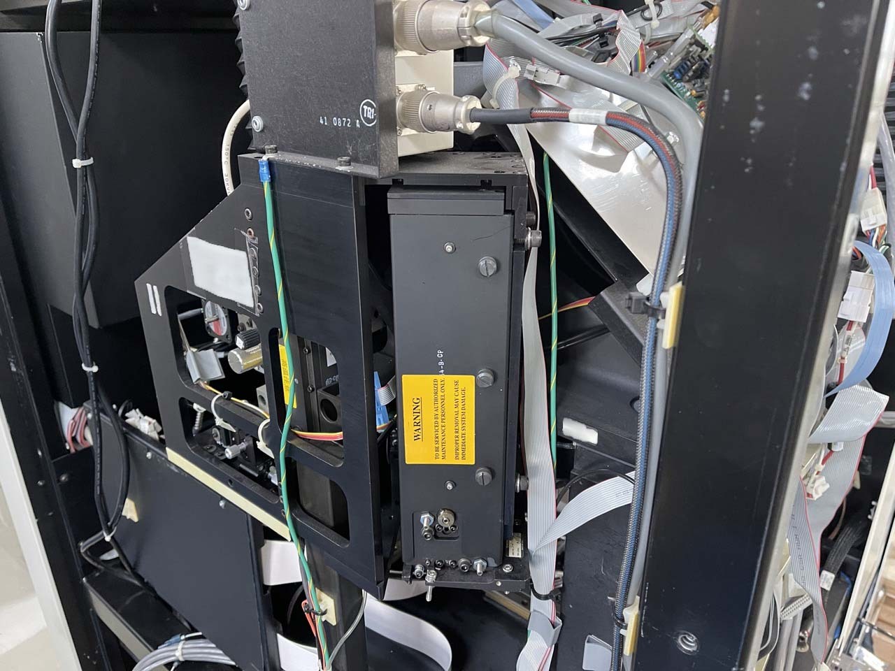
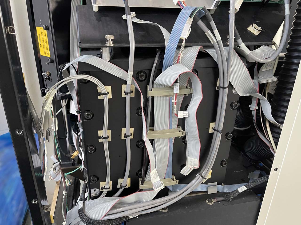
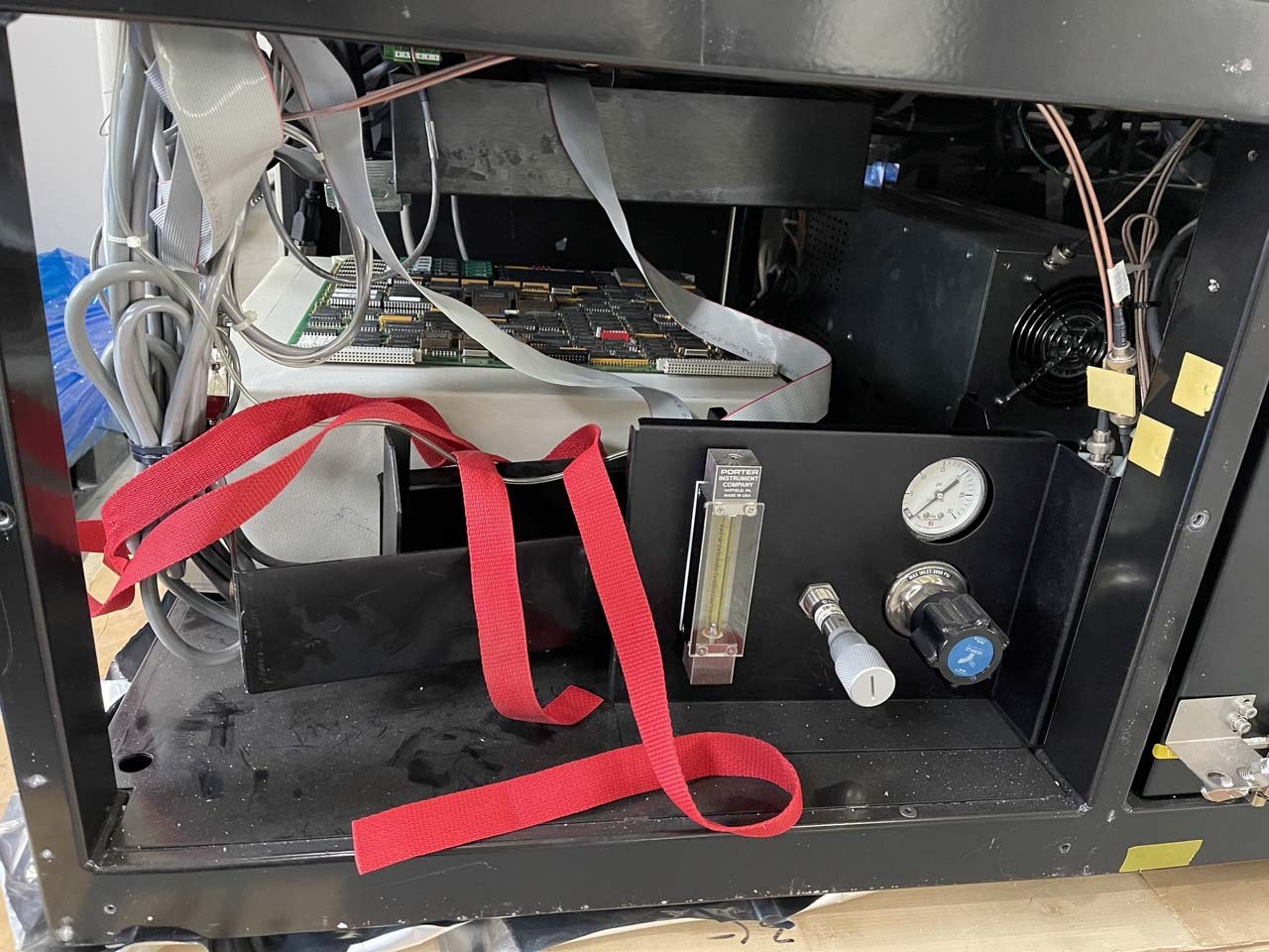
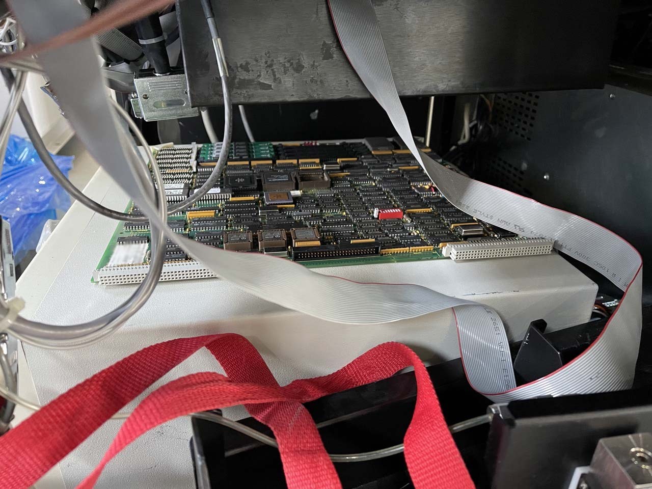
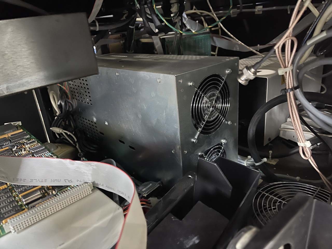
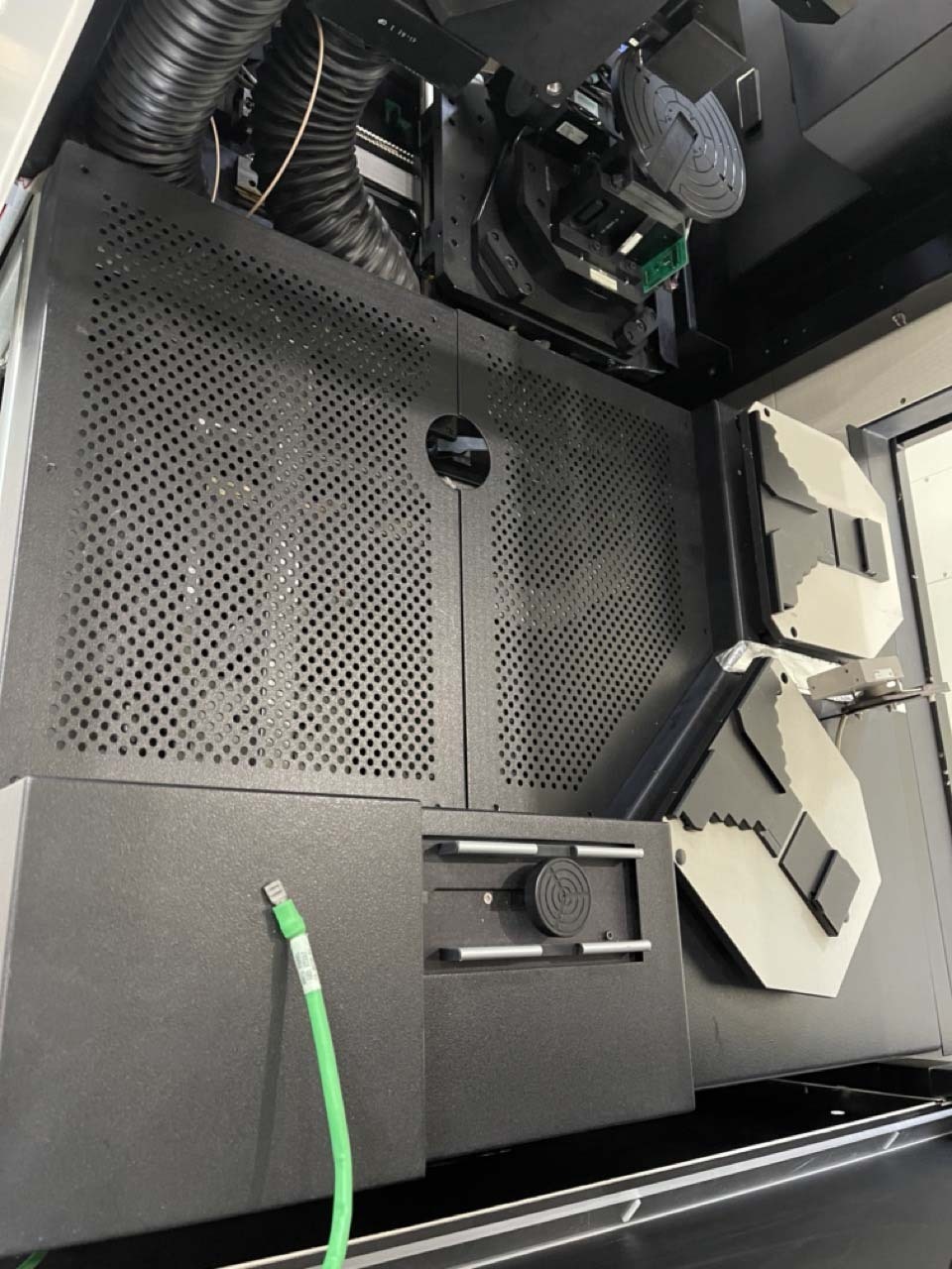
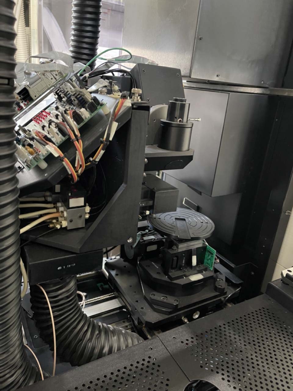
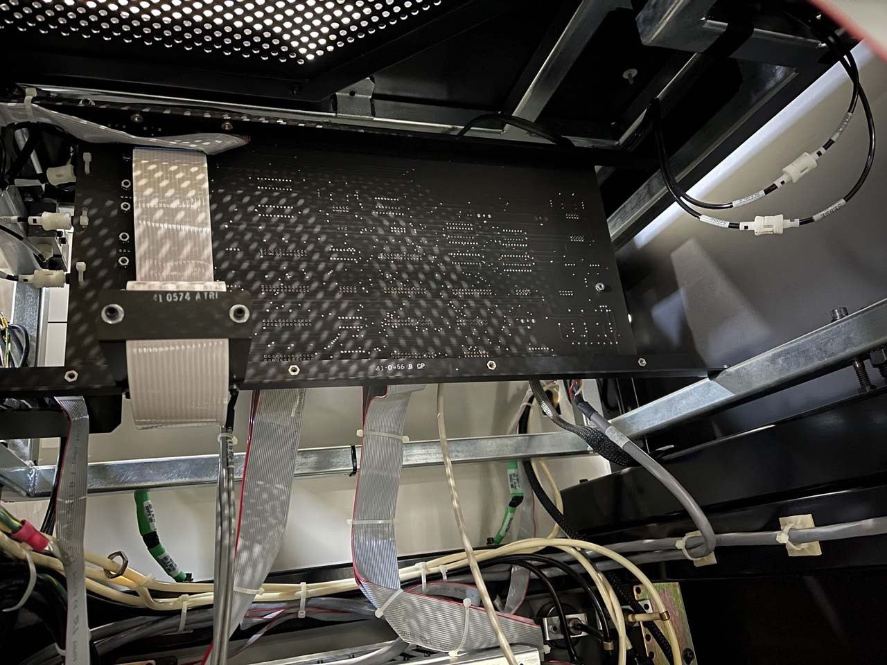
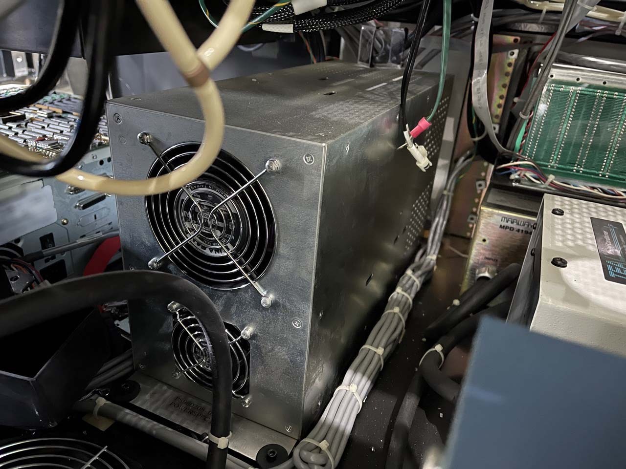
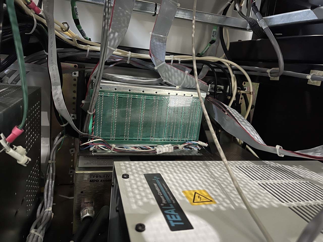
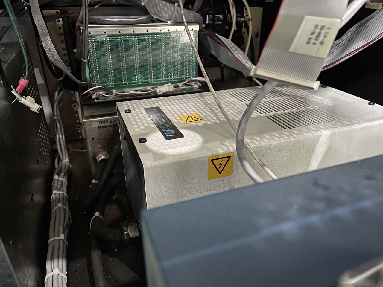
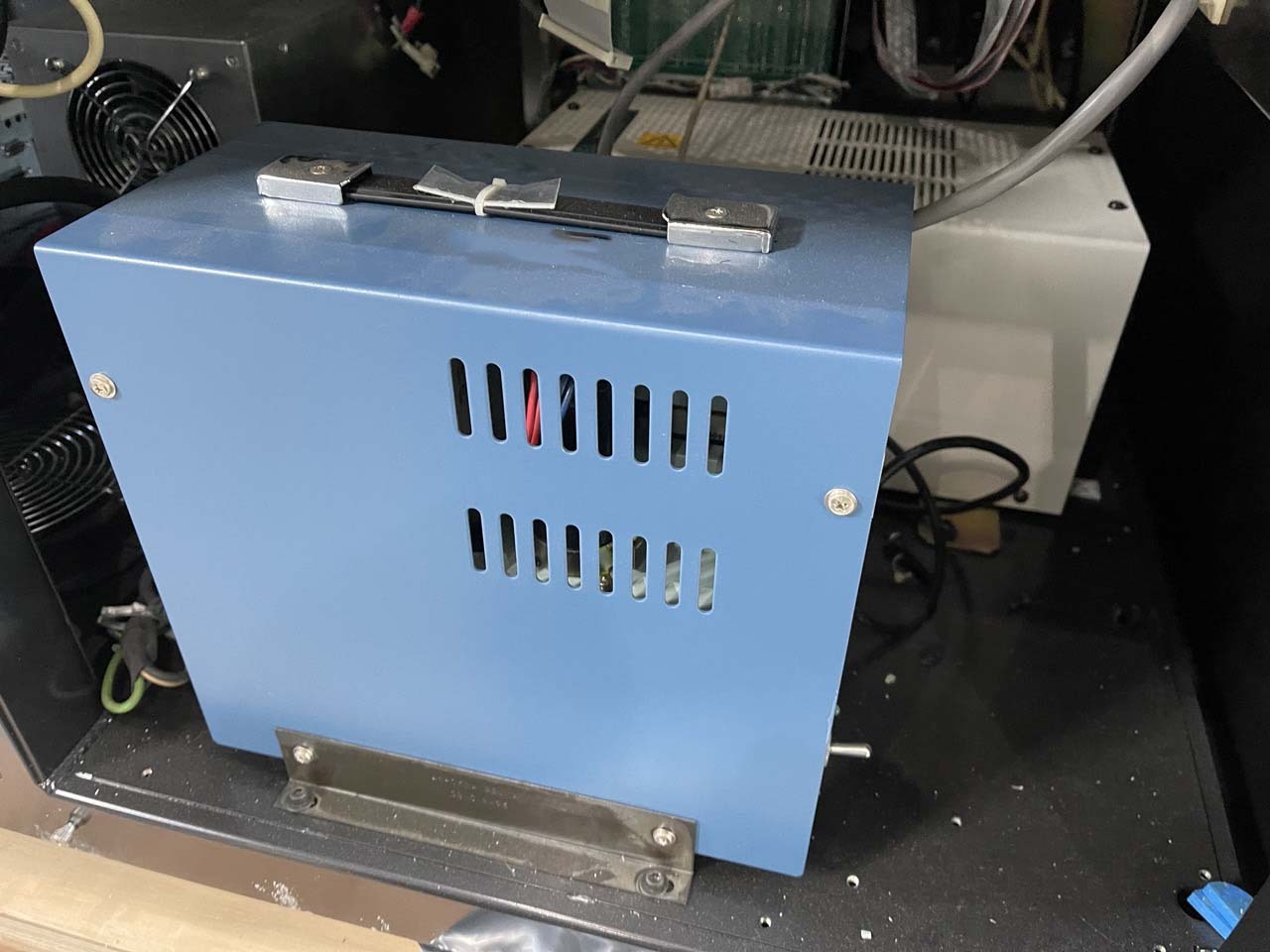
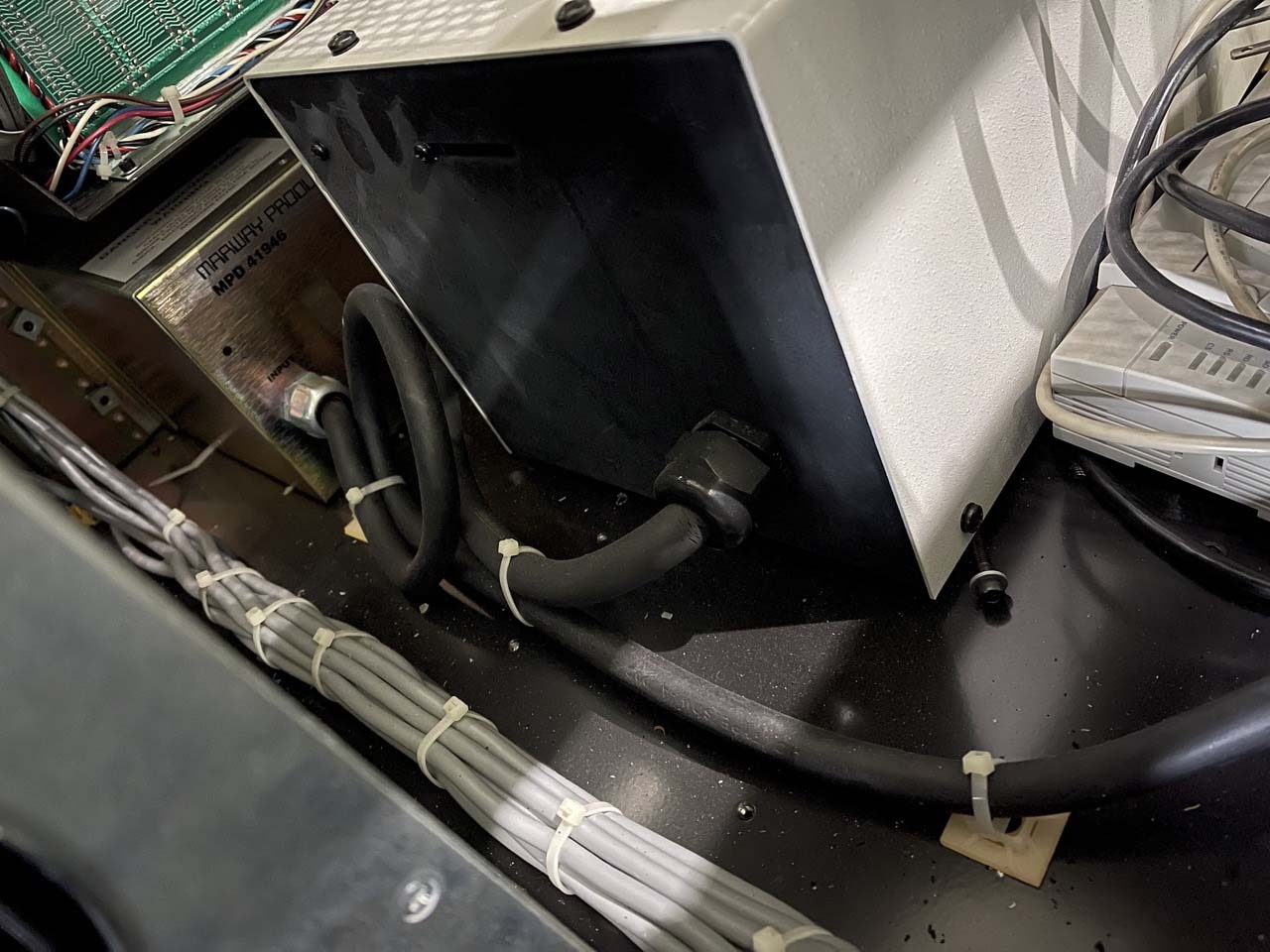
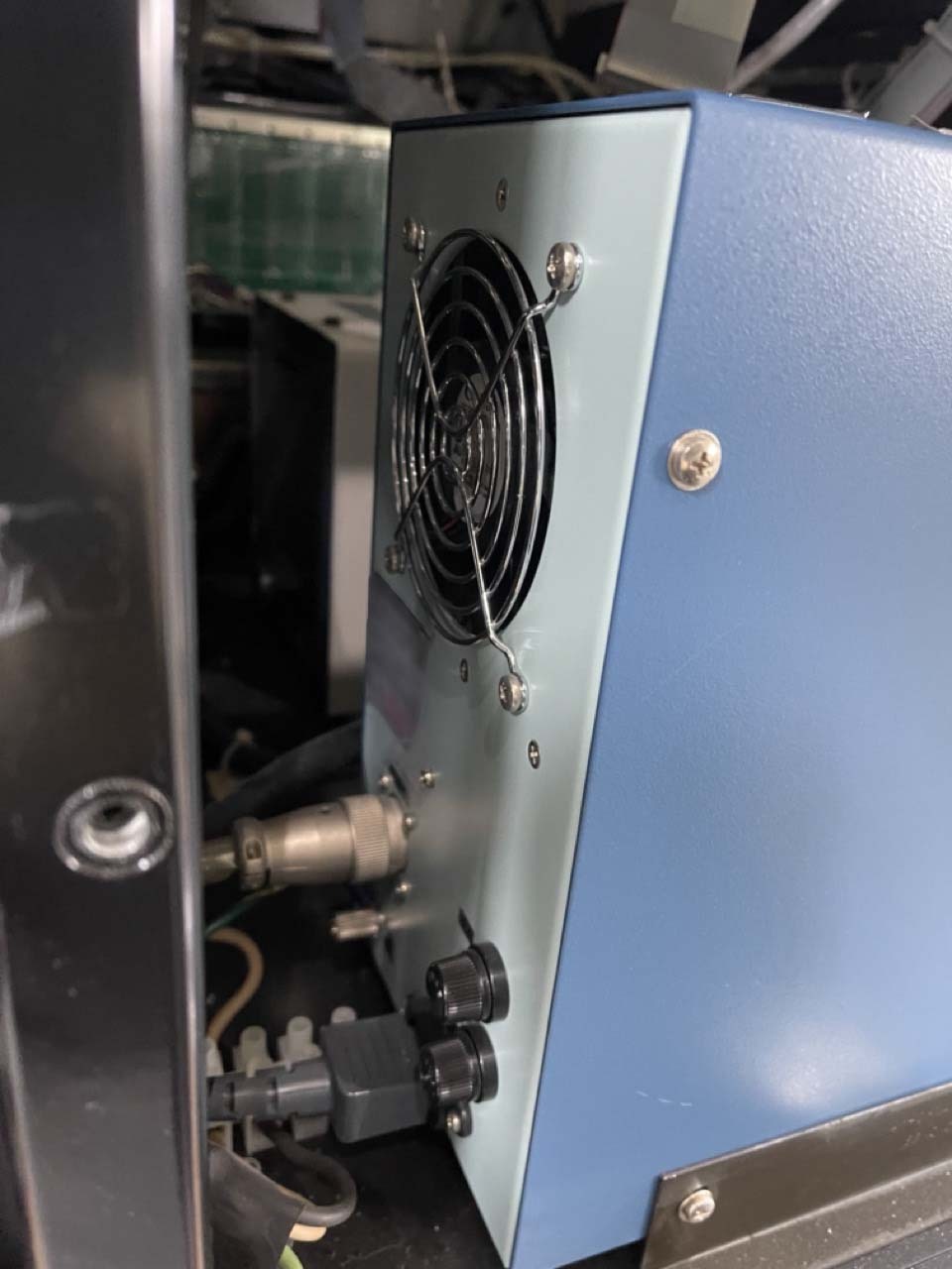
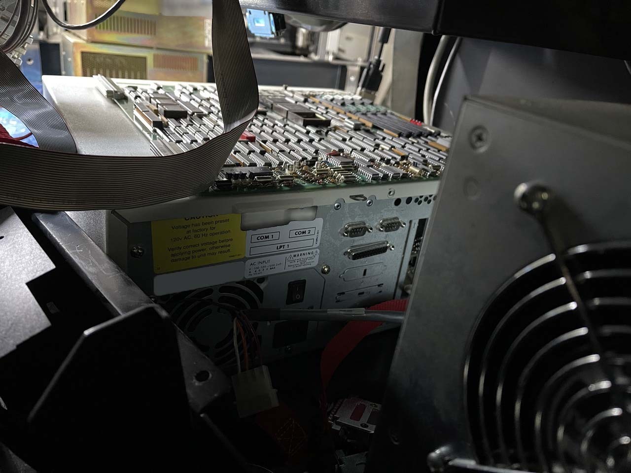
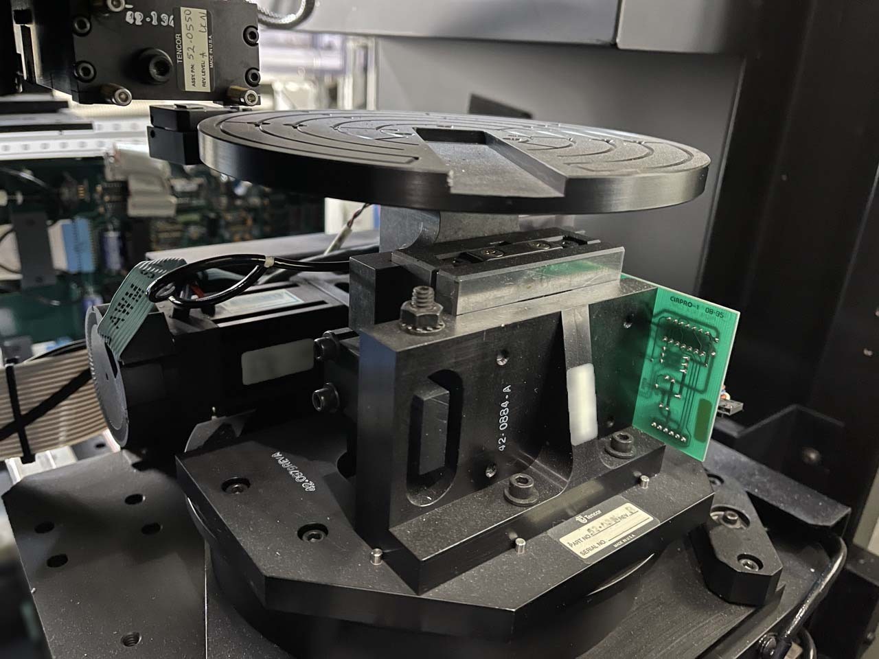
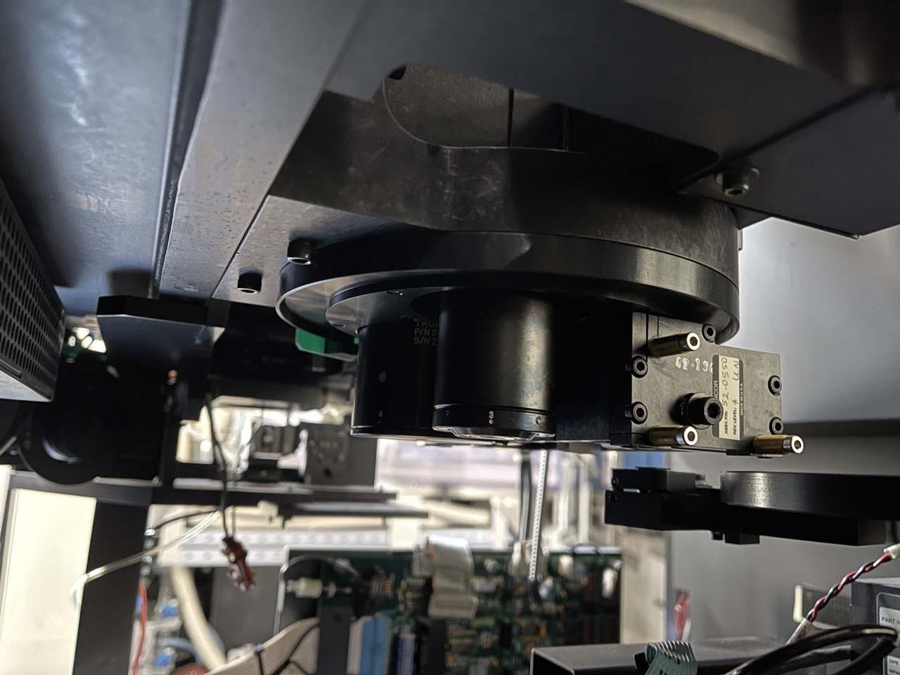
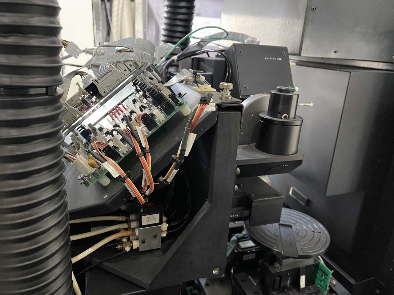
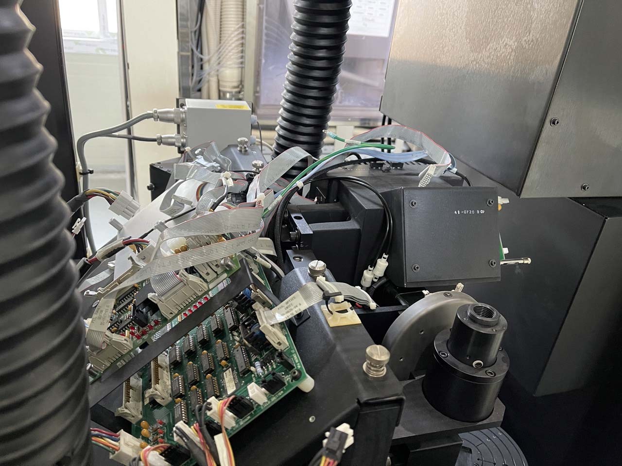
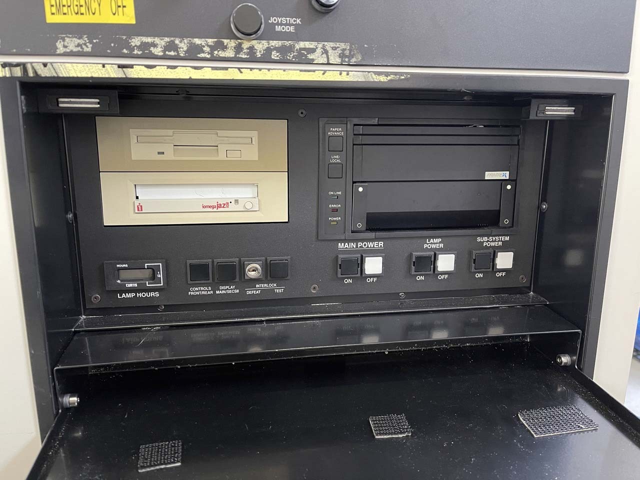
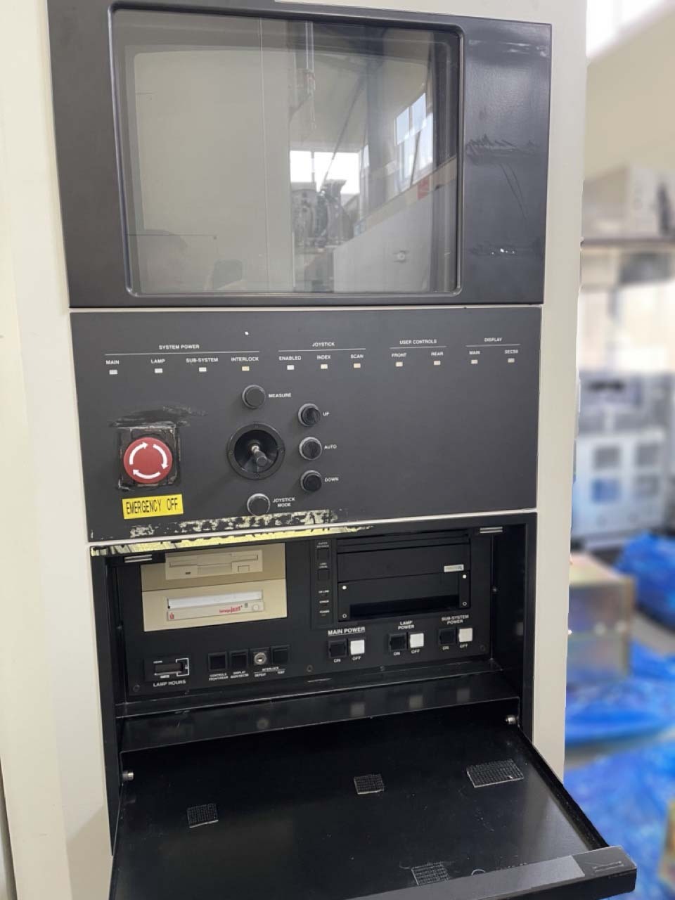
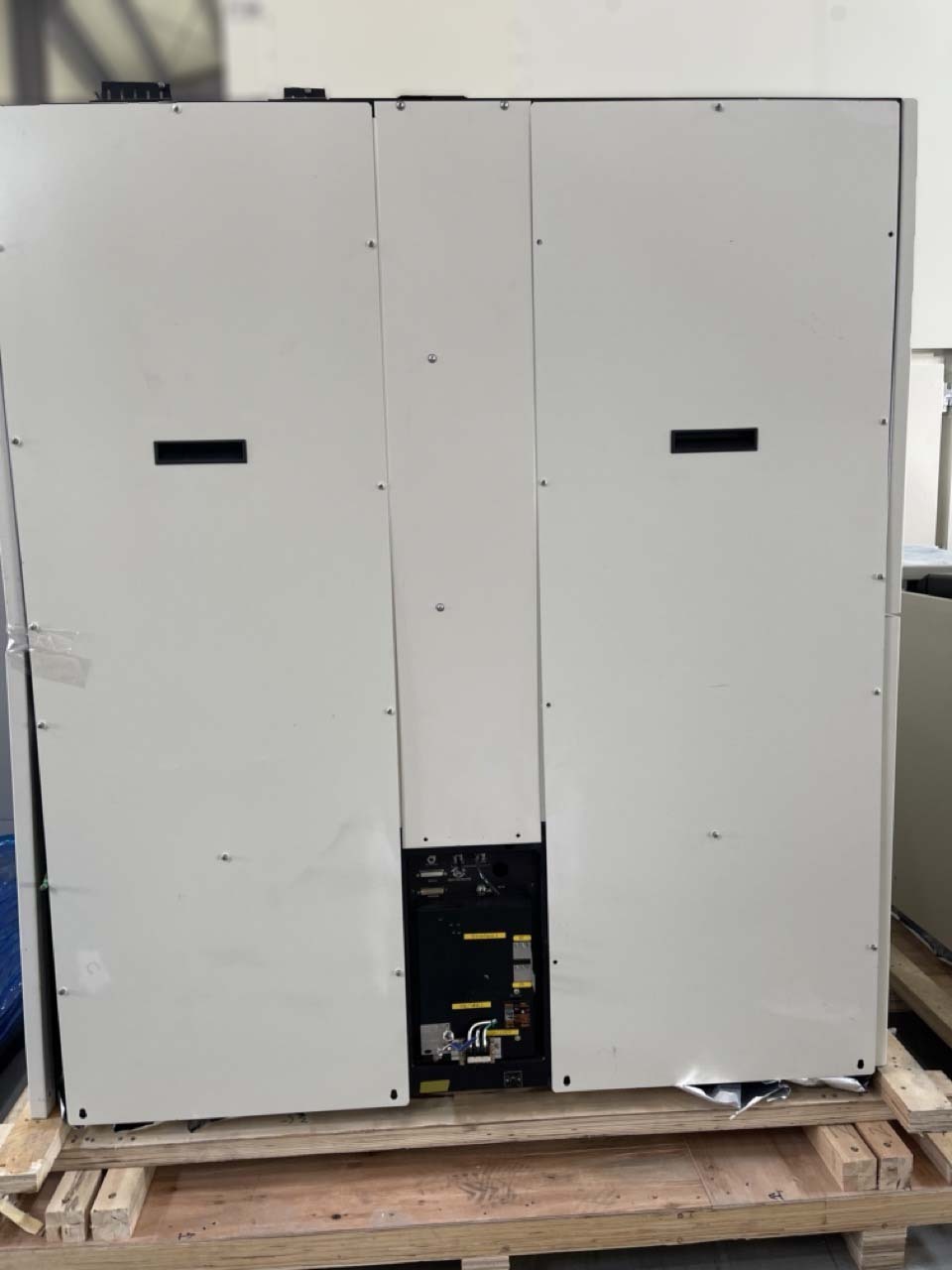
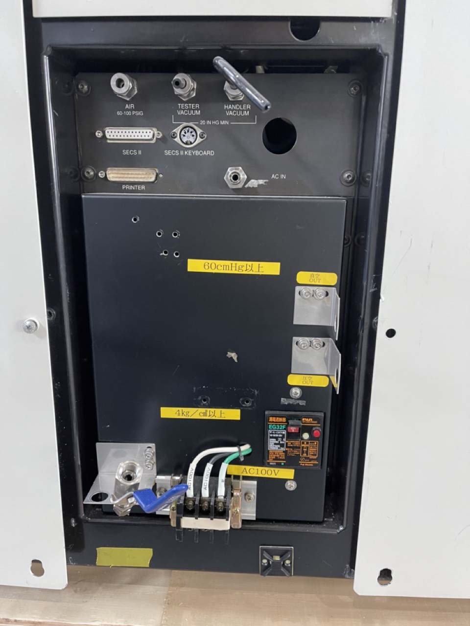
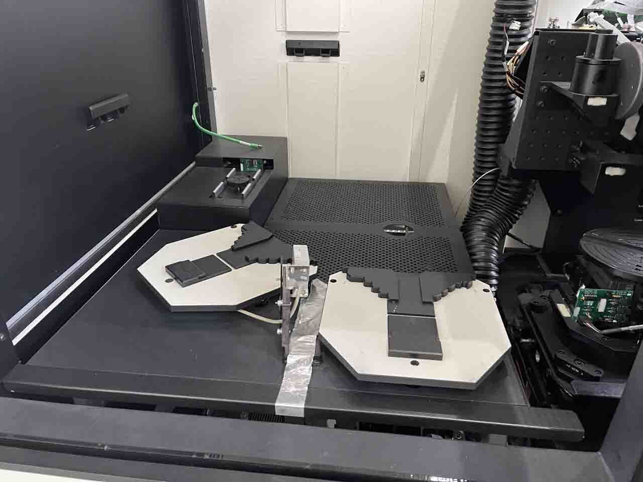
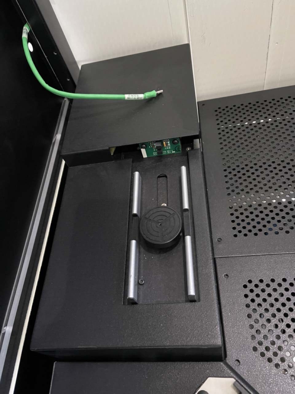
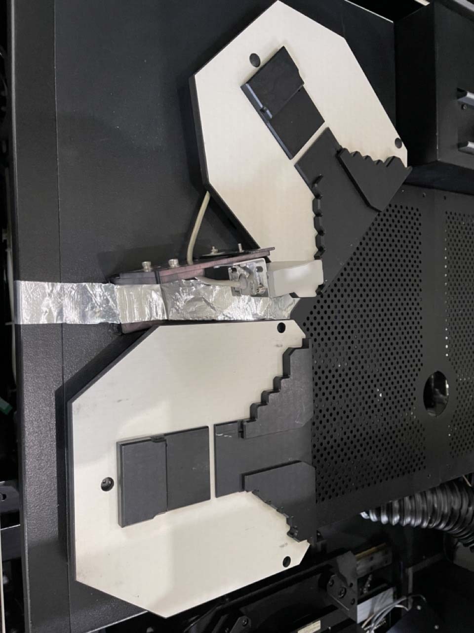
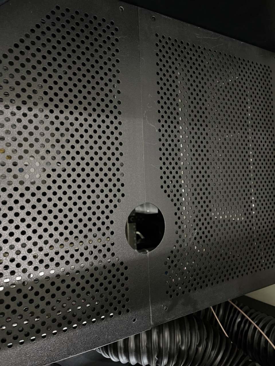
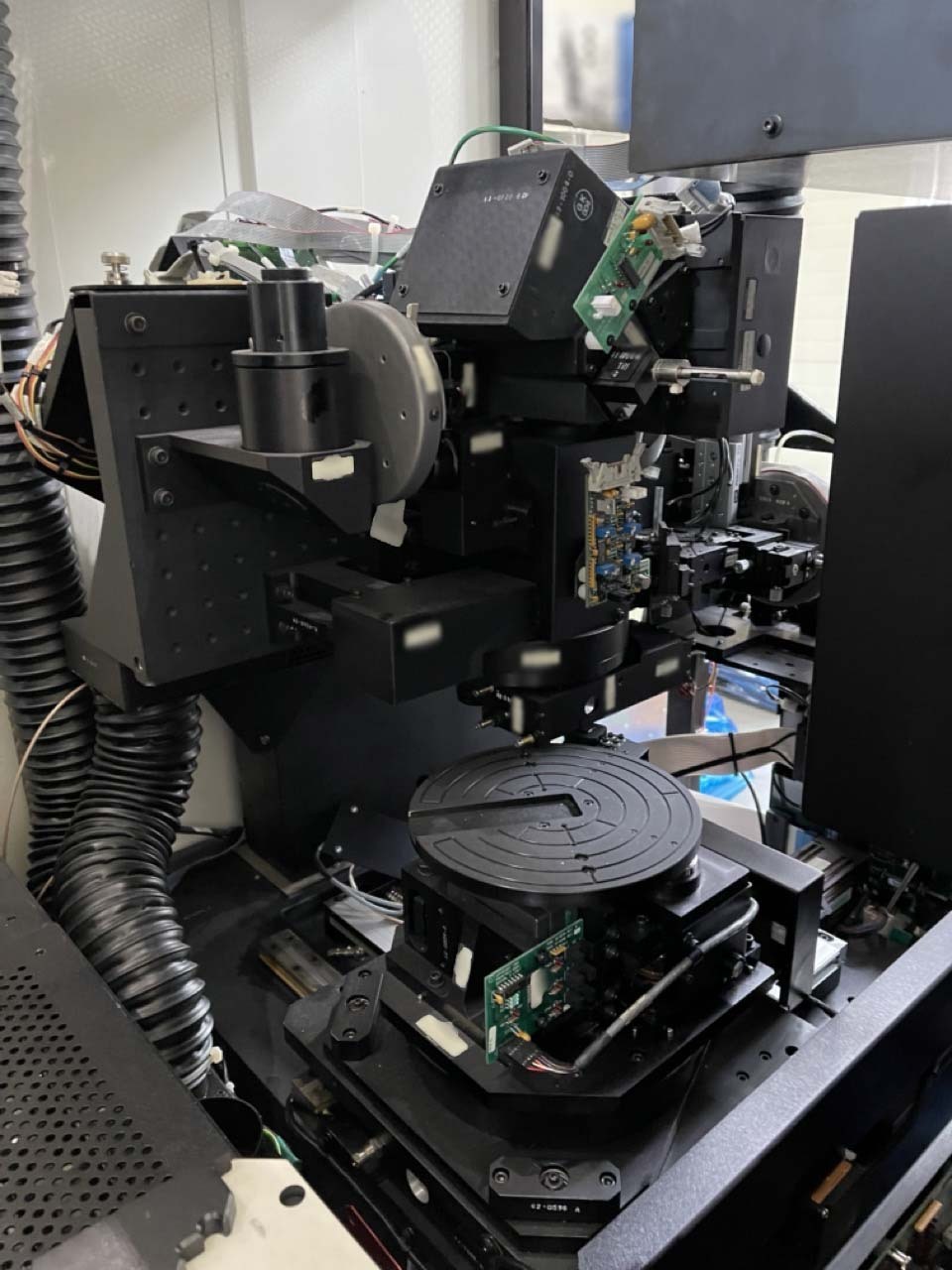
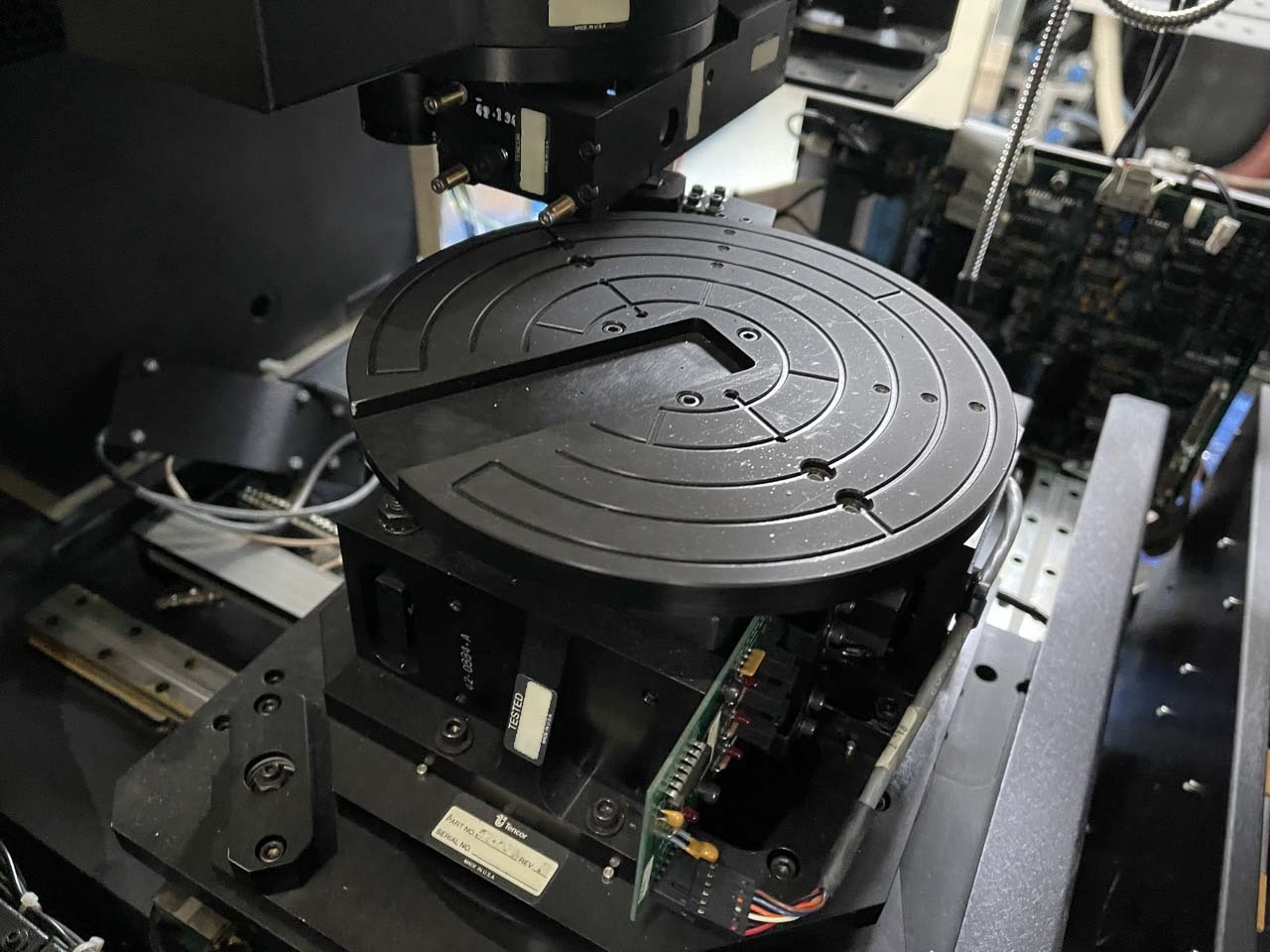
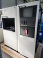
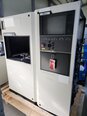
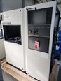
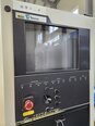
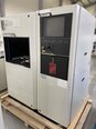
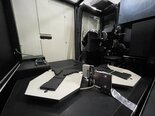
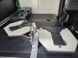
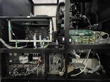
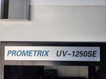
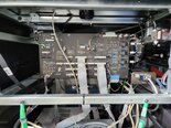
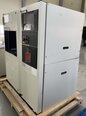
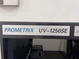
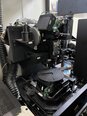
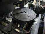
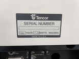
KLA / TENCOR UV 1250SE is an advanced wafer testing and metrology equipment designed for the semiconductor industry. This system integrates precision optics, advanced algorithms, and cutting-edge technologies to enable high-throughput and accurate measurement of various parameters on semiconductor wafers. KLA UV 1250SE is specifically tailored for the inspection and measurement of critical dimensions, defects, and thin film properties in the semiconductor manufacturing process. At the core of TENCOR UV1250SE unit is its advanced UV (ultraviolet) illumination source, which enables high-resolution imaging of semiconductor wafers with exceptional clarity and accuracy. This UV illumination source allows for precise detection and characterization of defects, pattern deviations, and other critical features on the wafer surface. Additionally, the UV wavelength range used in the machine is optimized for enhancing sensitivity to defects and critical dimensions, making it a powerful tool for process control and yield optimization in semiconductor manufacturing. UV1250SE tool is equipped with a high-performance optical asset that includes advanced imaging components such as lenses, mirrors, and filters to capture detailed images of the wafer surface. The optical model is carefully designed to minimize distortions and aberrations, ensuring accurate measurement and inspection results. Furthermore, the equipment features a high-speed image acquisition and processing capability, allowing for rapid scanning and analysis of wafers without compromising on accuracy or resolution. One of the key strengths of UV 1250SE system is its comprehensive suite of metrology algorithms and analysis tools. These advanced algorithms are specifically developed to extract critical information from the images captured by the unit, such as dimensions, overlay, depth, and material properties of features on the wafer. The machine can perform automated measurements of various parameters with high precision and repeatability, enabling semiconductor manufacturers to monitor and control their processes effectively. Moreover, TENCOR UV 1250SE tool offers a variety of inspection modes and measurement capabilities to accommodate different requirements in semiconductor manufacturing. For example, the asset can perform CD (critical dimension) measurements to assess the size and shape of patterns on the wafer, defect inspection to identify and classify defects on the surface, and film thickness measurements to determine the thickness of thin films deposited on the wafer. These capabilities make KLA / TENCOR UV1250SE a versatile tool for quality assurance and process optimization in semiconductor production. In addition to its advanced imaging and measurement capabilities, KLA UV1250SE model is designed for high productivity and ease of use in a manufacturing environment. The equipment features an intuitive user interface that allows operators to set up inspections, analyze results, and generate reports efficiently. It also includes sophisticated data analysis and visualization tools to help users interpret the measurement data and make informed decisions about process adjustments. Overall, KLA / TENCOR UV 1250SE is a state-of-the-art wafer testing and metrology system that offers exceptional performance, reliability, and versatility for semiconductor manufacturing. With its advanced UV imaging technology, precise measurement algorithms, and user-friendly interface, KLA UV 1250SE is a valuable tool for ensuring the quality and integrity of semiconductor wafers throughout the production process.
There are no reviews yet