Used KLA / TENCOR XP2 #293814733 for sale
URL successfully copied!
Tap to zoom
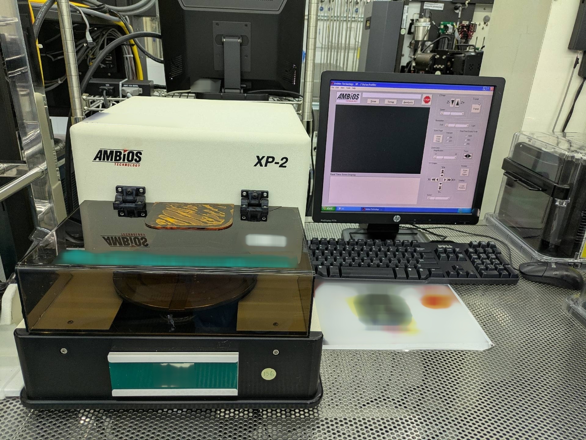

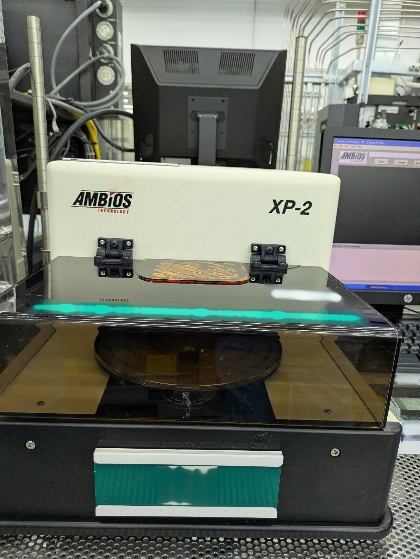
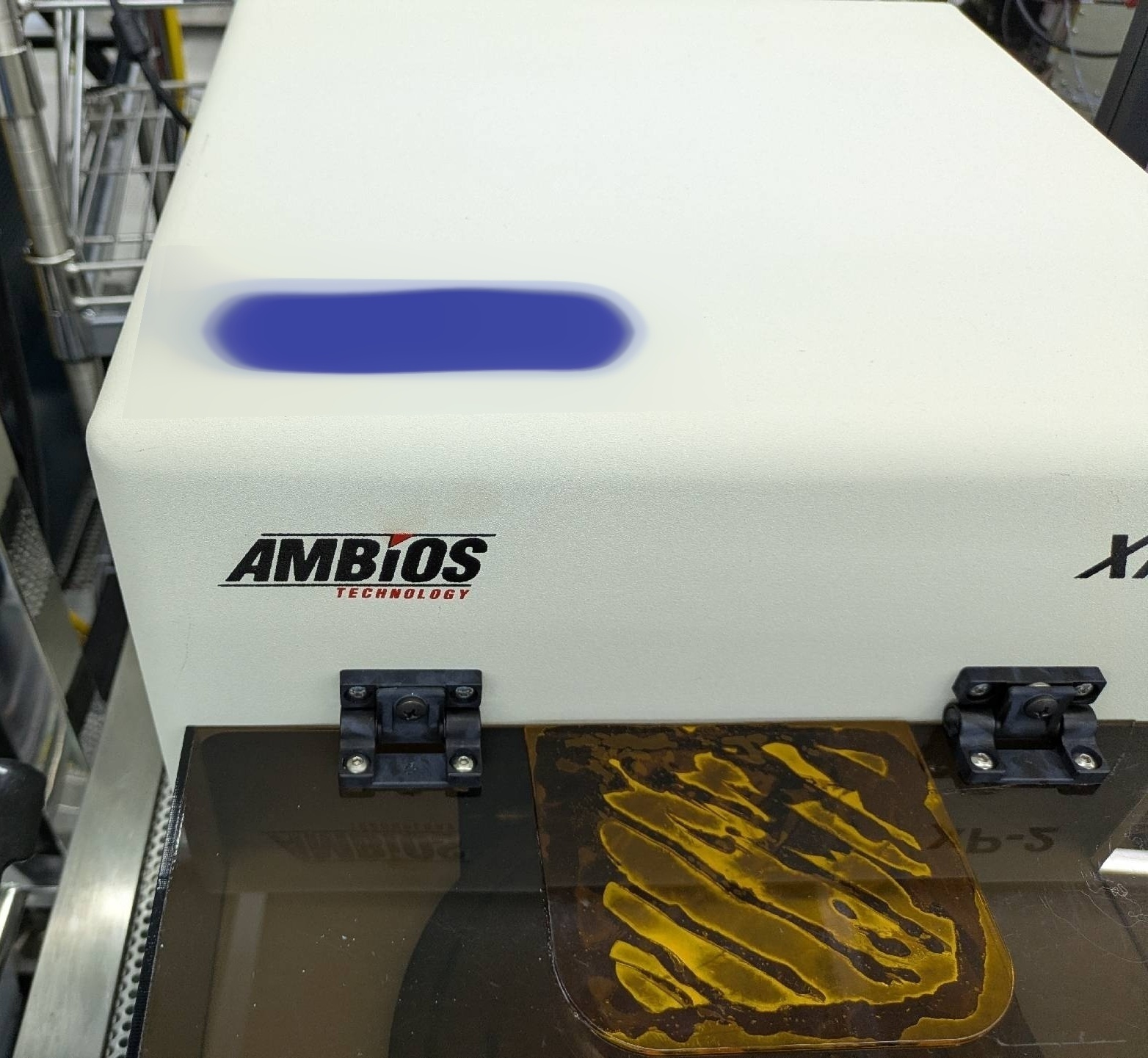
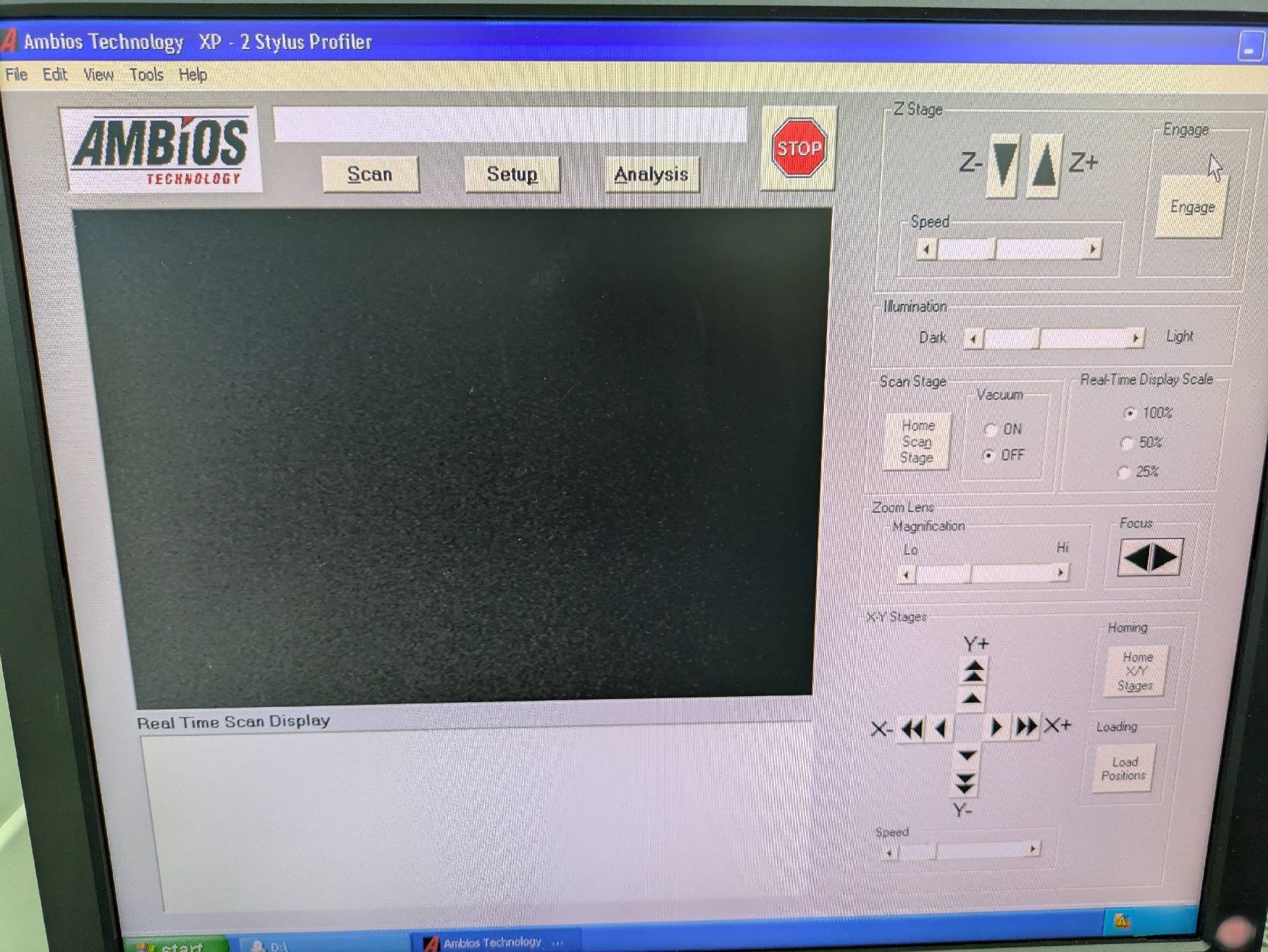
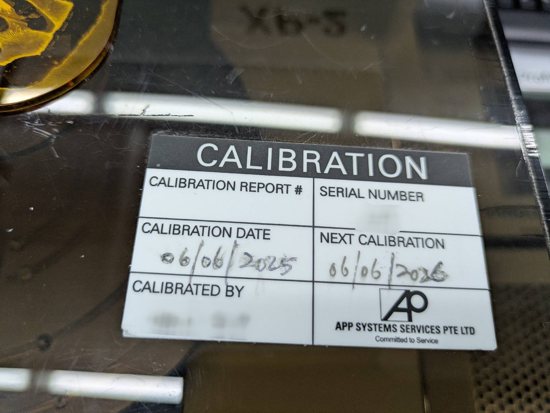
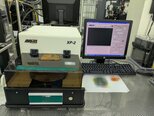
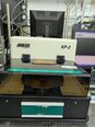
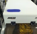
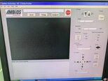
KLA / TENCOR XP-2 is a wafer testing and metrology equipment used in semiconductor manufacturing lines for quality assurance and yield enhancement. It is designed for fast, comprehensive, non-destructive wafer measurements of 300mm wafers. KLA XP-2 system employs a wide array of wafer surface scanning techniques, such as optical or profile non-contact metrology measurements, to generate reliable wafer measurements quickly and accurately. Optical scanning arms are used to generate fast, quantitative bright field or dark field imaging to capture edge fidelity, surface topography, planarity, flatness, saw-tooth defects, line or space widths, critical dimension errors, and other factors related to wafer parameters. The data can be converted into a highly detailed 3-D model for further analysis. In addition to the optical systems, TENCOR XP-2 has advanced metrology capabilities such as a critical dimension channel station and line width or edge profile station. These metrology tools use precise air-bearing scanning to measure critical dimensions or line widths and edge profiles quickly and accurately. The model is also equipped with advanced defect inspection capabilities, which can be used to detect particle defects, crystal defects, and other surface inconsistencies. The particle defect inspection unit is designed to generate very high-resolution defect images at high throughput in order to accurately detect and identify particle defects on the wafer surface. Furthermore, XP-2 is equipped with an extensive set of process, test, and yield analysis tools. It can accurately measure critical parameters such as wafer handling time, wafer dopping, loading error, or yield loss per wafer. It can also help to identify excessive costs due to yield loss or test time inefficiencies. KLA / TENCOR XP-2 is a powerful and reliable wafer testing and metrology machine that provides data-driven solutions to many of the problems faced by semiconductor manufacturers. It offers precision wafer surface scanning for accurate wafer measurement in addition to advanced defect inspection and process analysis capabilities. Its advanced features enable semiconductor manufacturers to significantly reduce wafer production costs and increase yield.
There are no reviews yet