Used KOBELCO / LEO HRBS #293750091 for sale
URL successfully copied!
Tap to zoom
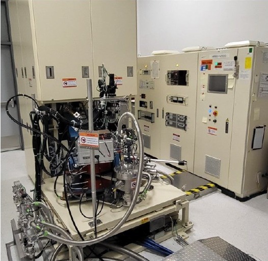

KOBELCO / LEO HRBS is an innovative wafer testing and metrology equipment developed by LEO and KOBELCO, designed to meet the rigorous requirements of semiconductor manufacturing processes. This system combines advanced technology and precision engineering to deliver comprehensive testing and metrology capabilities for semiconductor wafers, enabling manufacturers to achieve enhanced productivity, efficiency, and quality control. At the core of LEO HRBS unit is its wafer handling and positioning capabilities, which are crucial for ensuring accurate testing and measurement of semiconductor devices. The machine is equipped with high-precision robotic arms and advanced alignment systems that allow for precise positioning of wafers during testing, minimizing errors and improving overall measurement accuracy. KOBELCO HRBS tool features a range of testing modules that cover a wide variety of parameters critical to semiconductor device performance. These modules include electrical testing, optical inspection, and surface metrology capabilities, providing manufacturers with a comprehensive suite of tools for characterizing wafer properties and identifying defects or irregularities that may impact device functionality. One of the key strengths of HRBS asset is its ability to perform non-destructive testing on semiconductor wafers, allowing manufacturers to gather critical data without compromising the integrity of the devices under test. This non-destructive testing capability is essential for ensuring the reliability and quality of semiconductor devices, as it enables manufacturers to identify potential issues early in the manufacturing process and take corrective action before defects become critical. In addition to its testing capabilities, KOBELCO / LEO HRBS model is equipped with advanced metrology tools that enable manufacturers to characterize the physical and chemical properties of semiconductor wafers with high precision. These metrology tools include technologies such as scanning electron microscopy (SEM), atomic force microscopy (AFM), and spectroscopic techniques, which can provide detailed information on the surface morphology, composition, and structure of semiconductor materials. LEO HRBS equipment is designed with a user-friendly interface and intuitive software that streamline the testing and measurement process, making it easy for operators to set up tests, run experiments, and analyze data. The system also features advanced data processing and visualization tools that enable manufacturers to extract valuable insights from the test results and optimize their manufacturing processes for improved performance and efficiency. Overall, KOBELCO HRBS unit represents a cutting-edge solution for wafer testing and metrology in the semiconductor industry. With its advanced technology, precision engineering, and comprehensive capabilities, this machine empowers manufacturers to achieve higher levels of productivity, quality control, and operational excellence in semiconductor device manufacturing.
There are no reviews yet