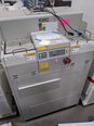
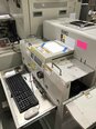
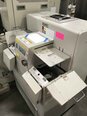
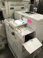
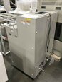
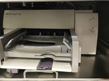
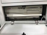
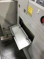
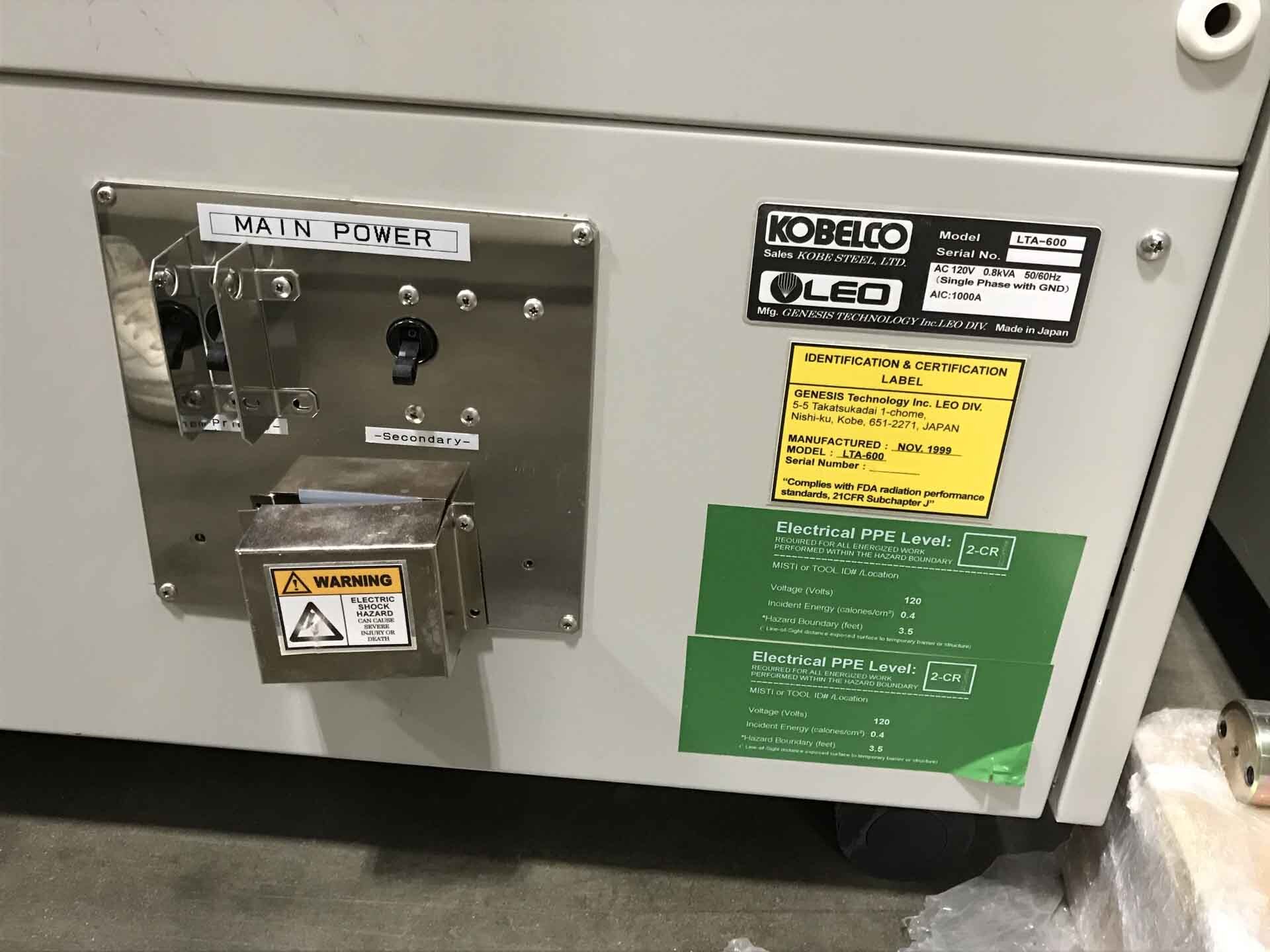
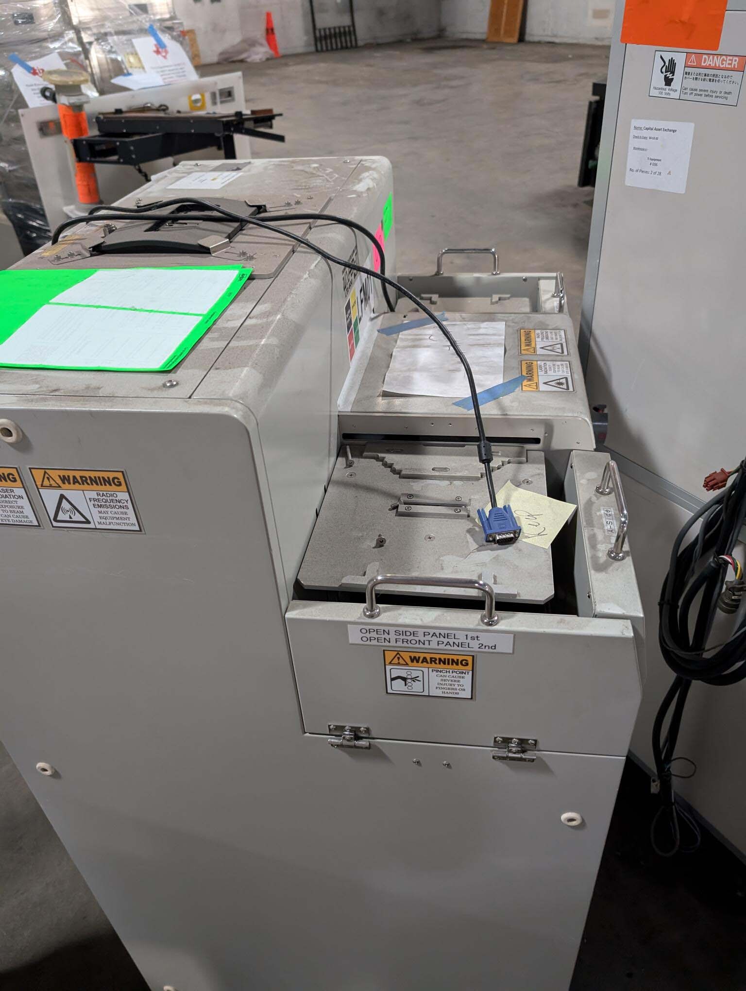
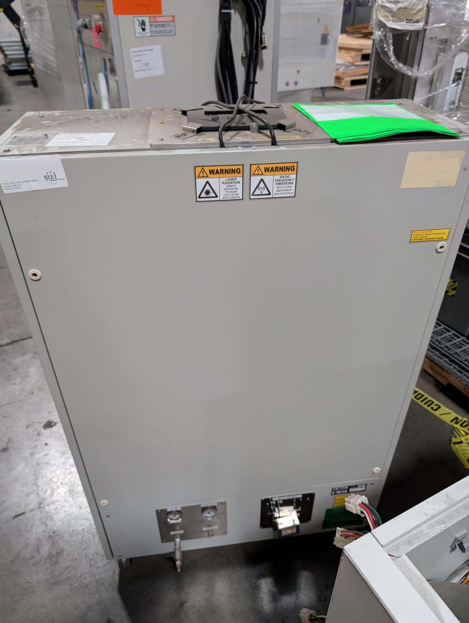
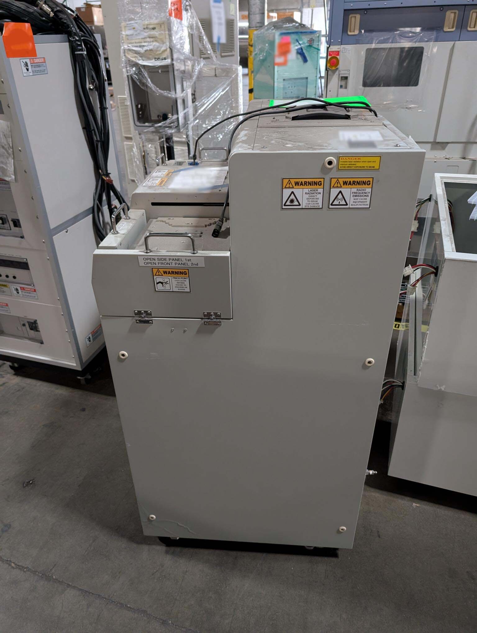
Used KOBELCO / LEO LTA-600 #9300841 for sale
URL successfully copied!

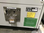
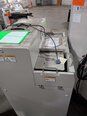
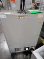
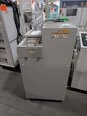
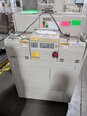
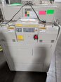
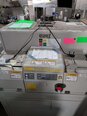
Tap to zoom
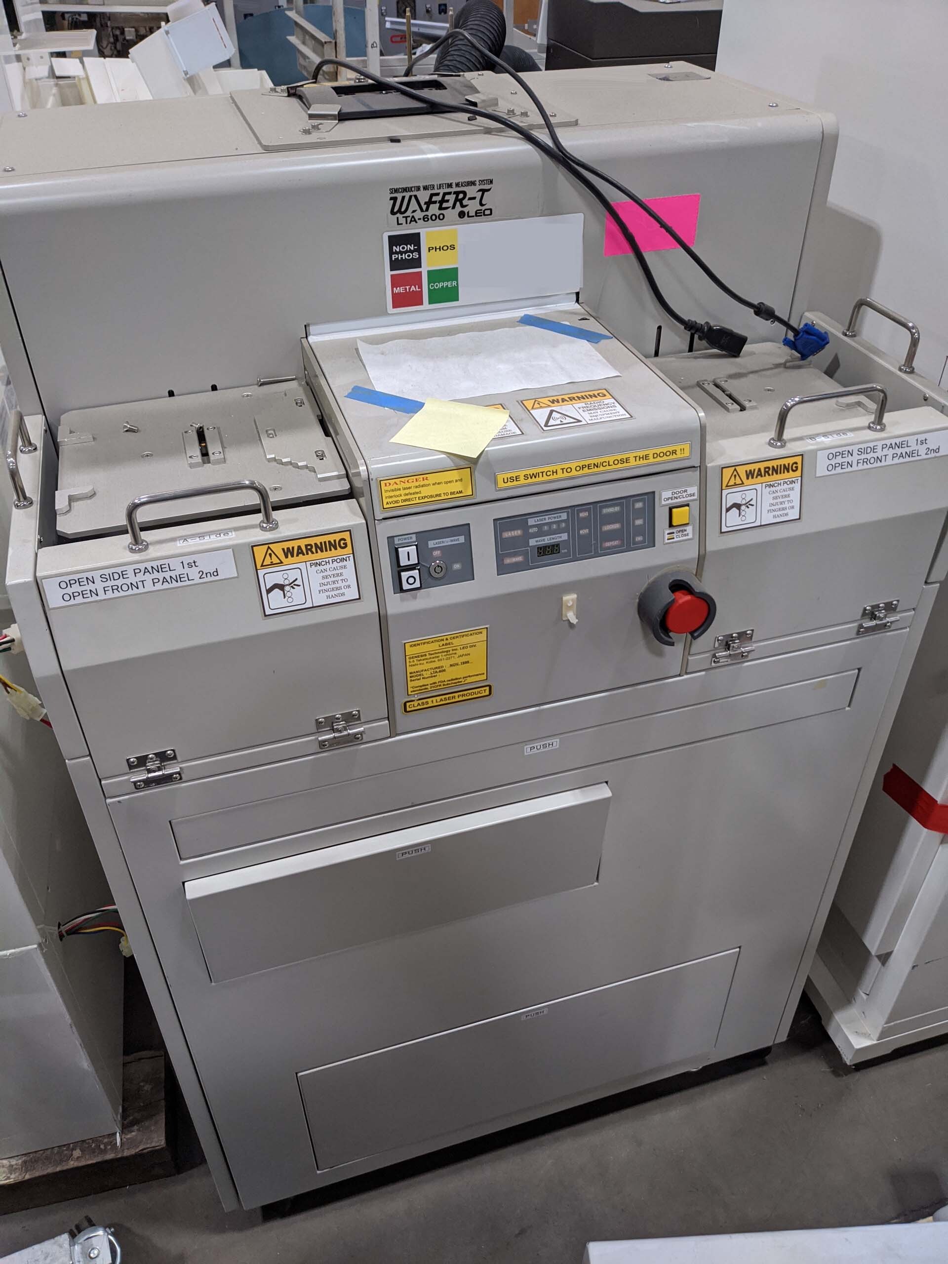

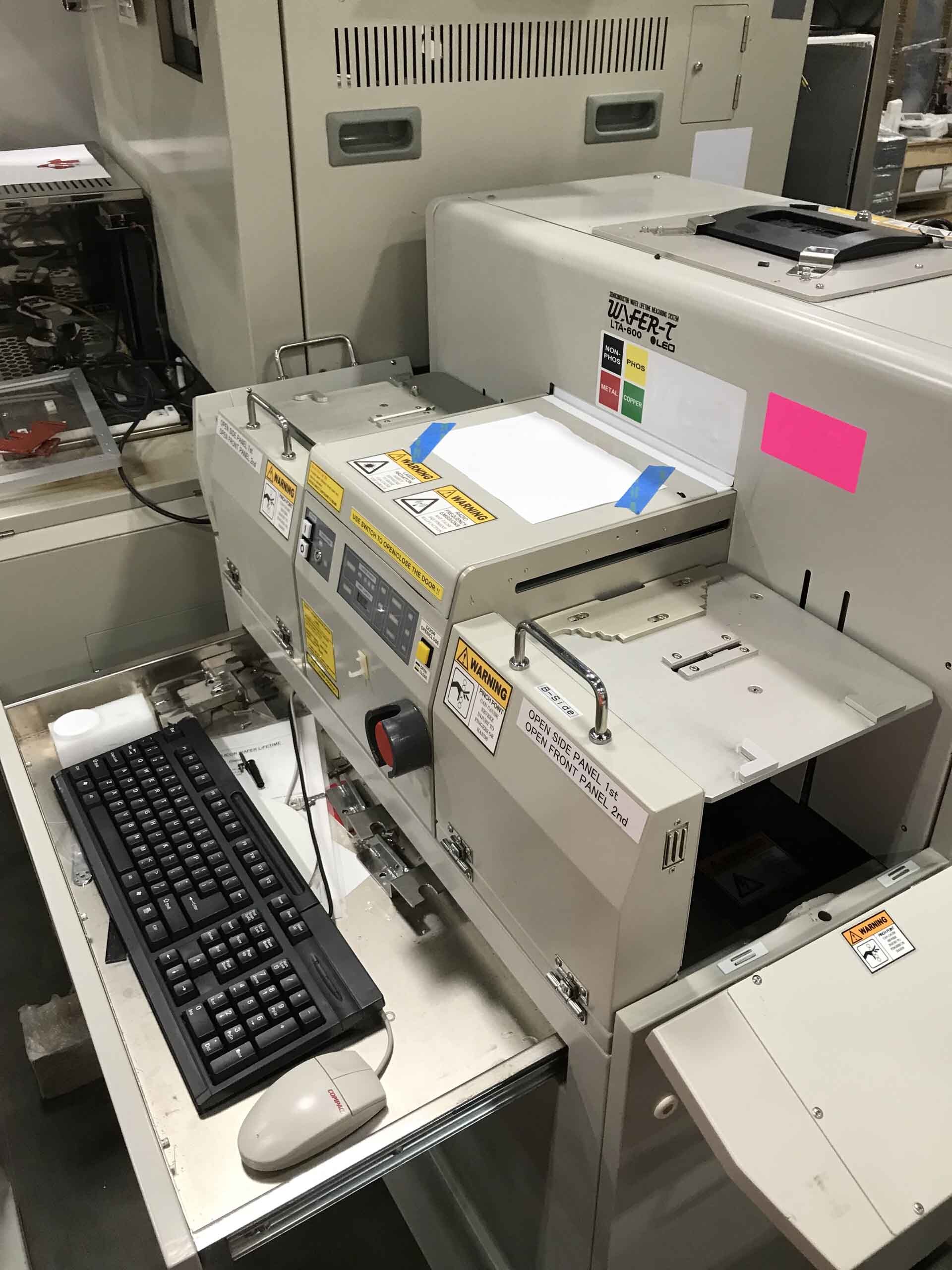
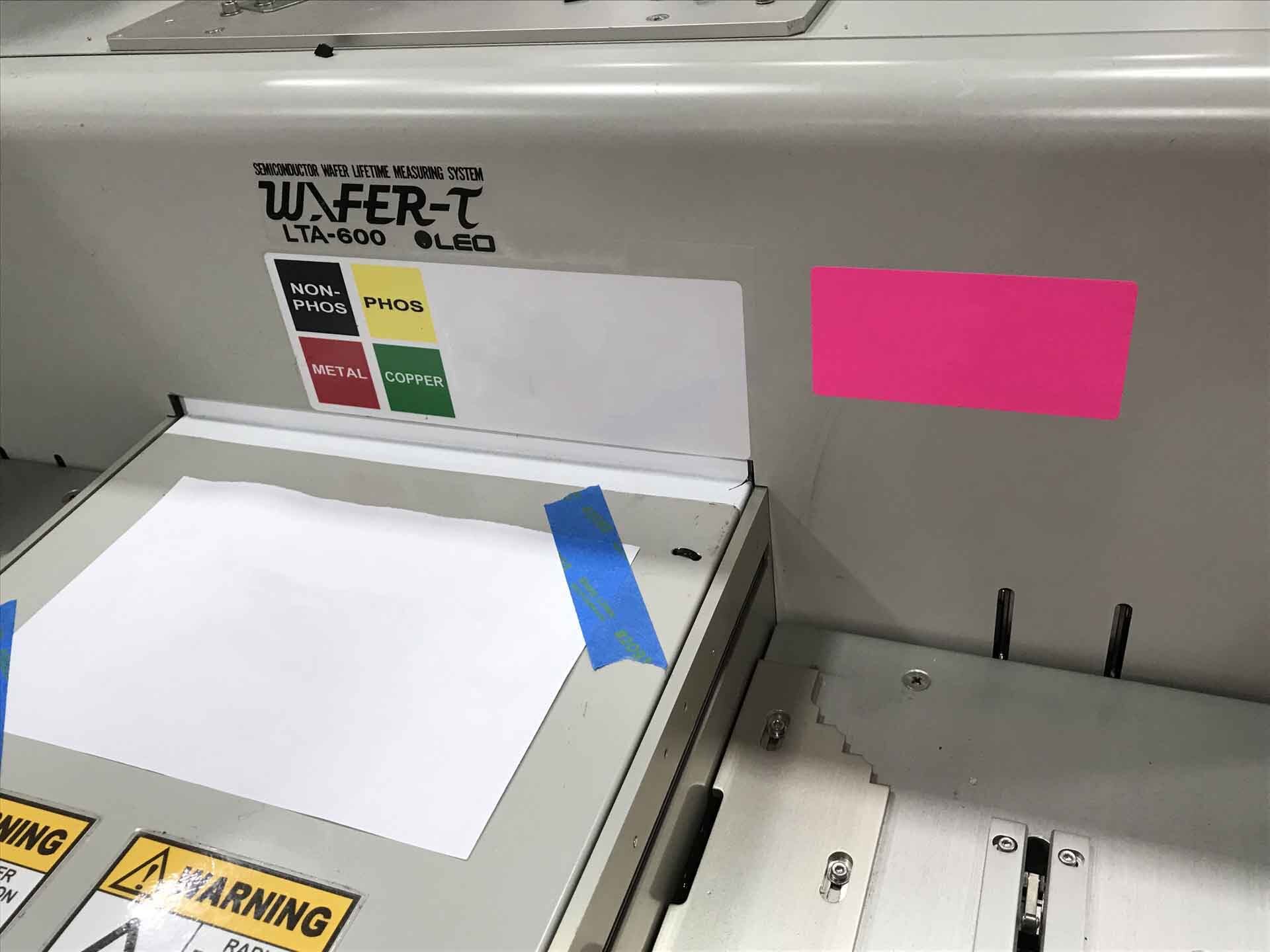
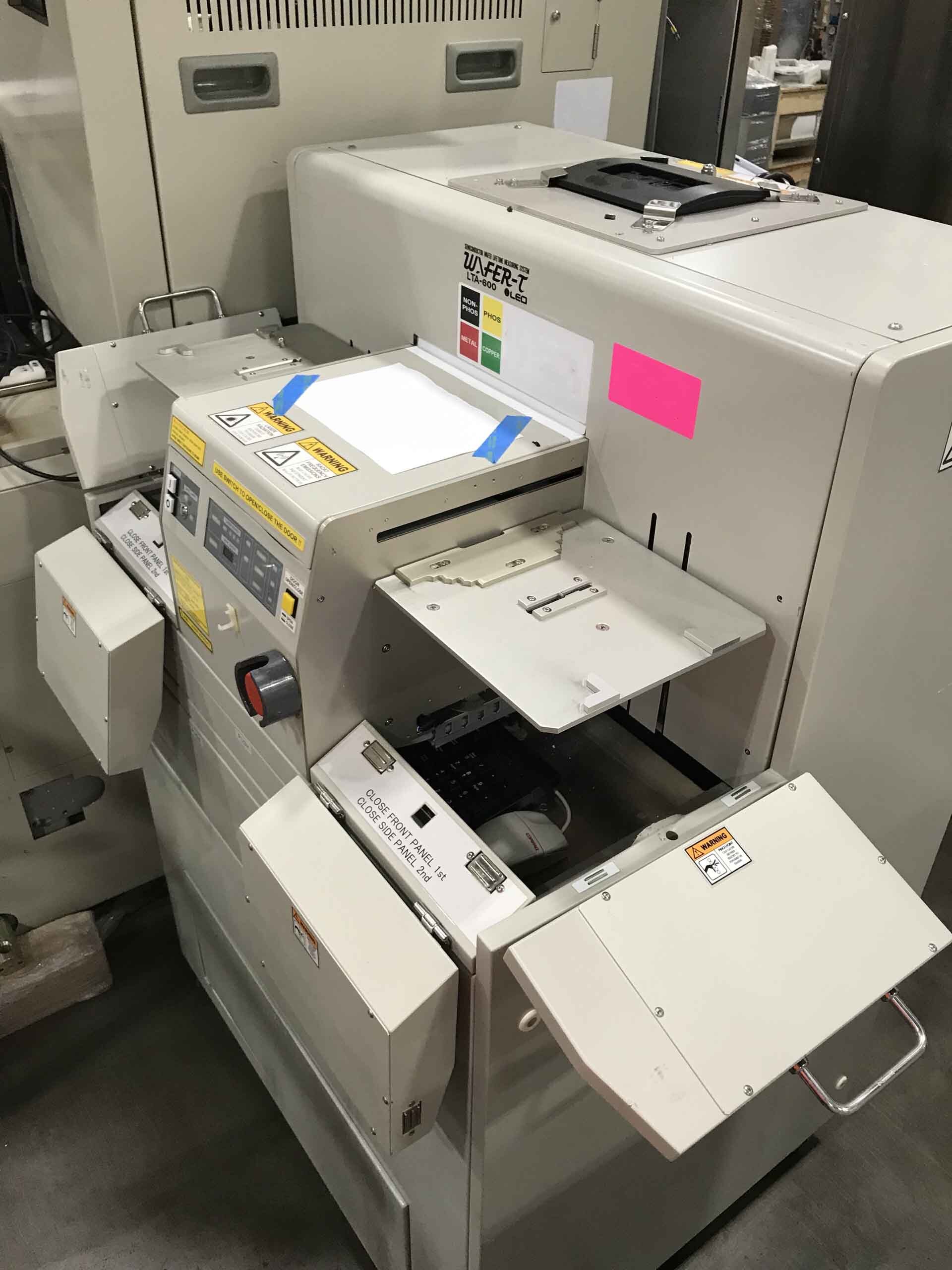
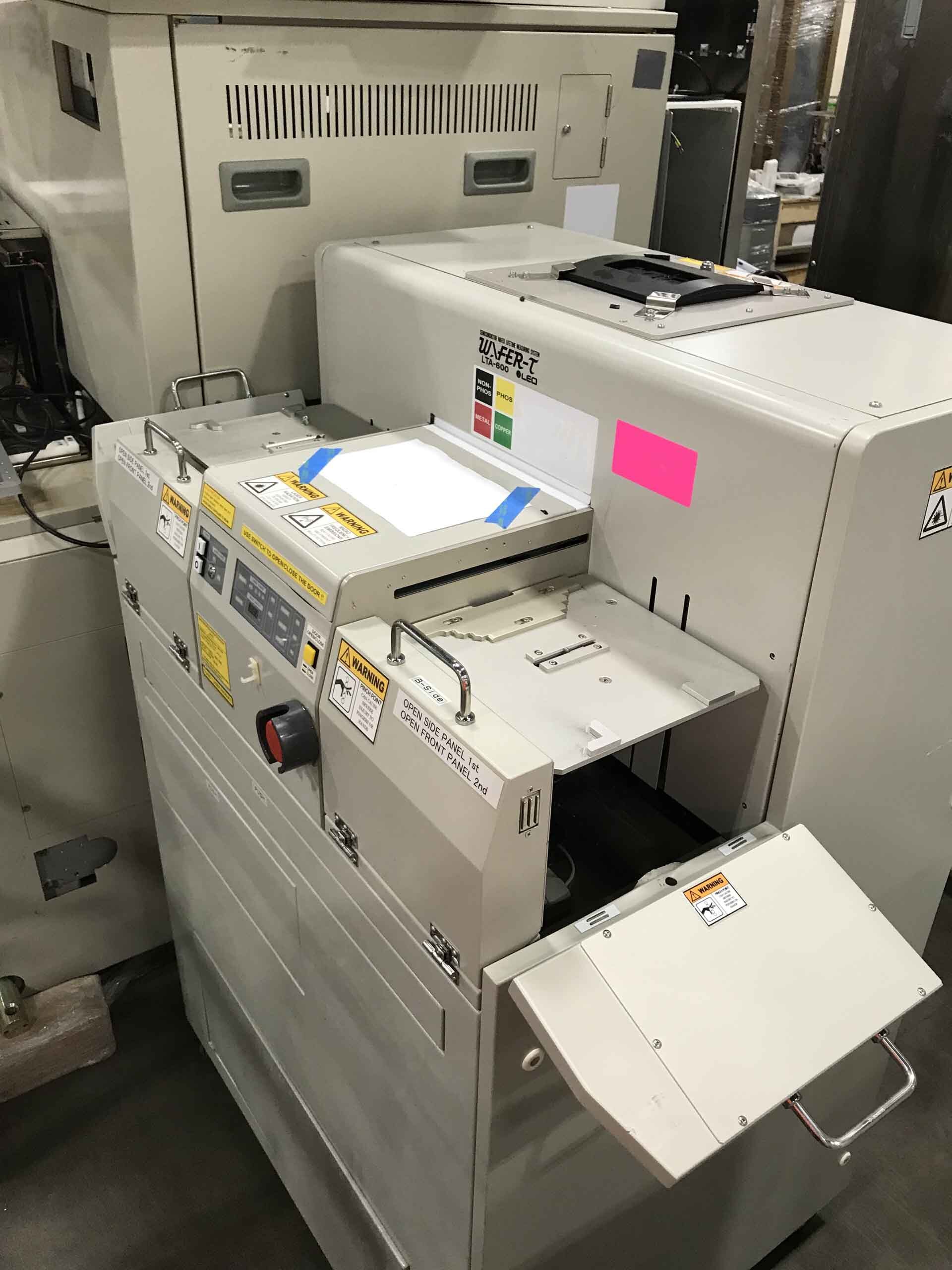
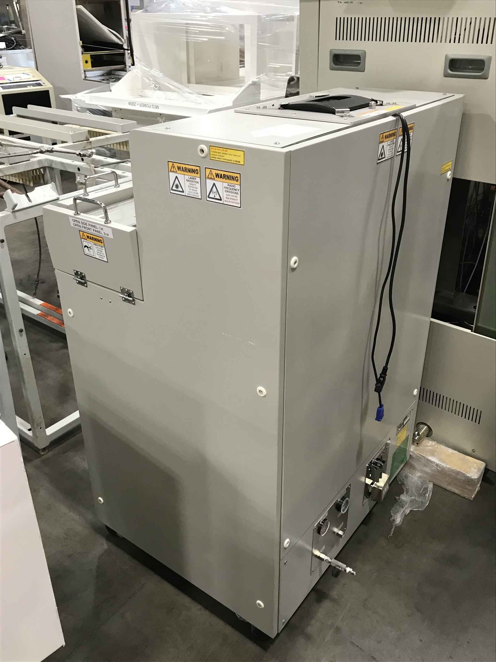
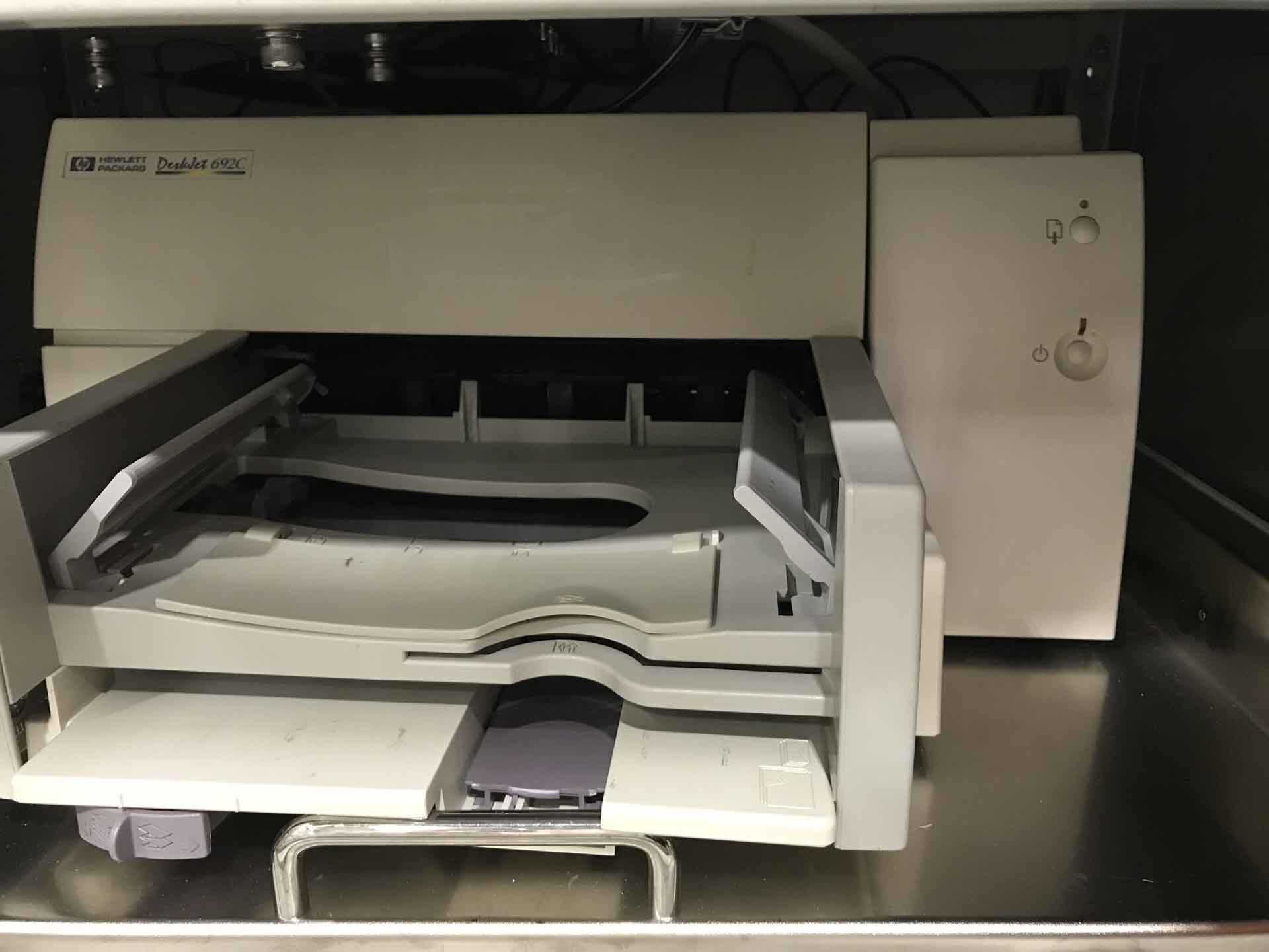
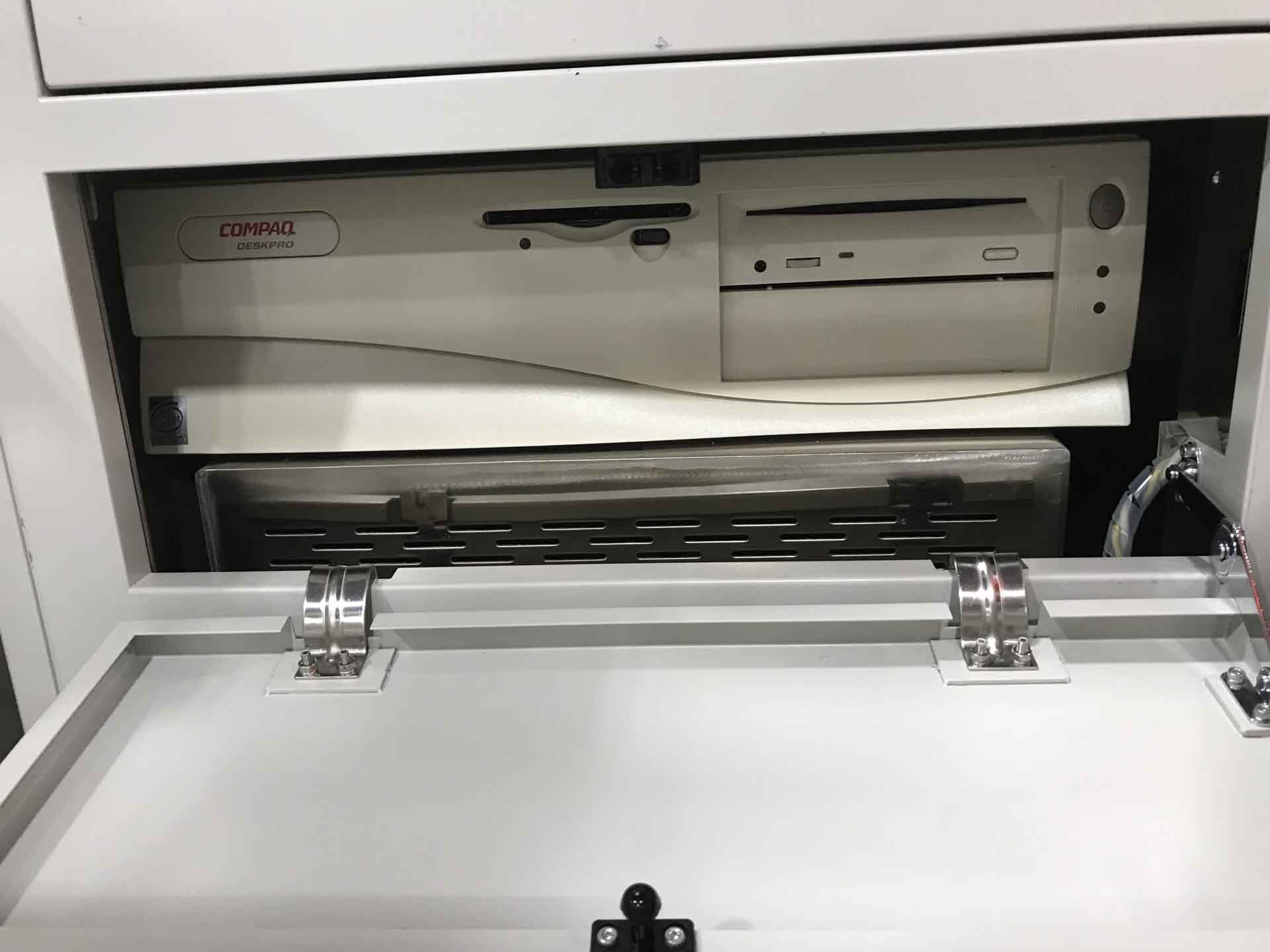
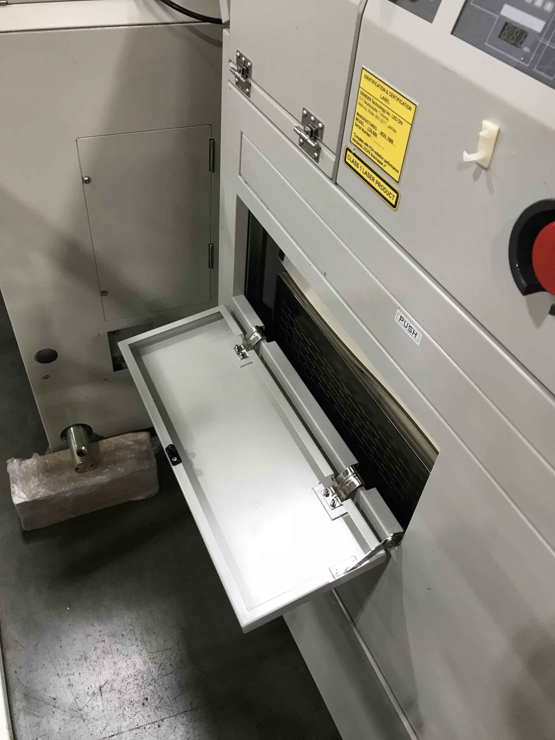
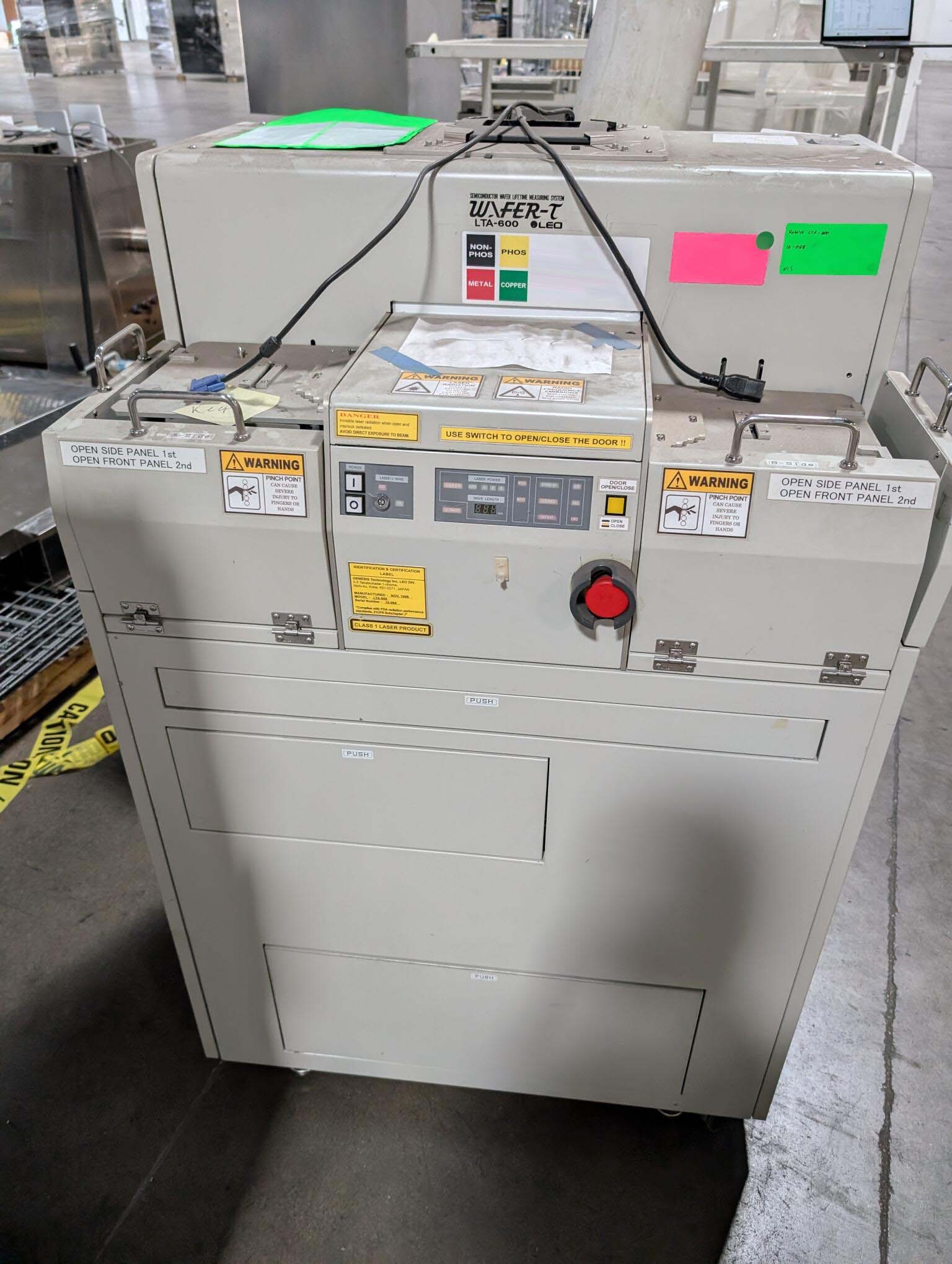
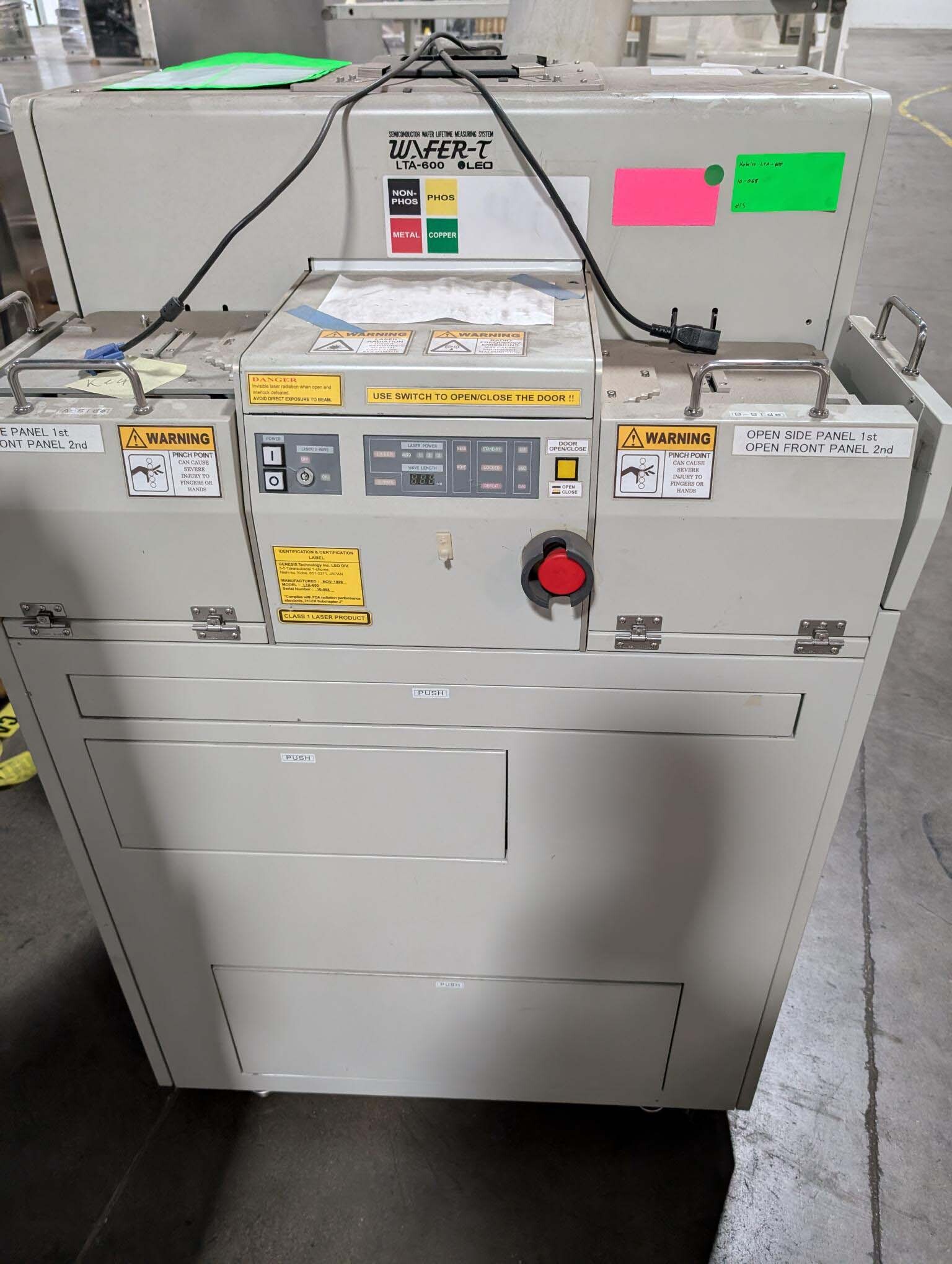
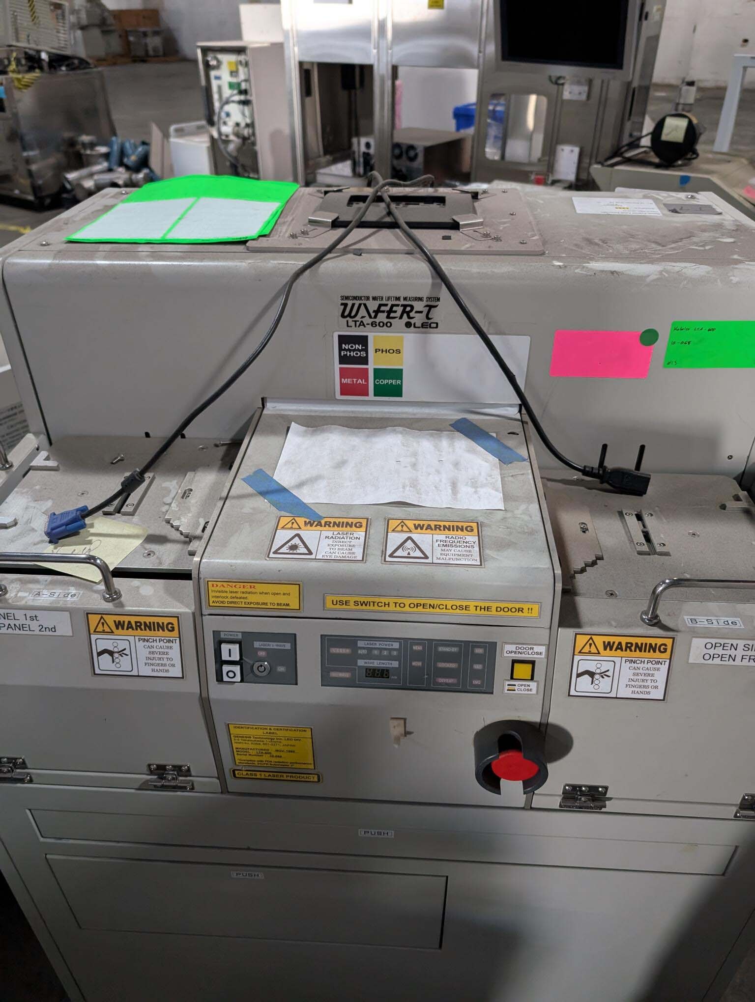
ID: 9300841
Wafer Size: 8"
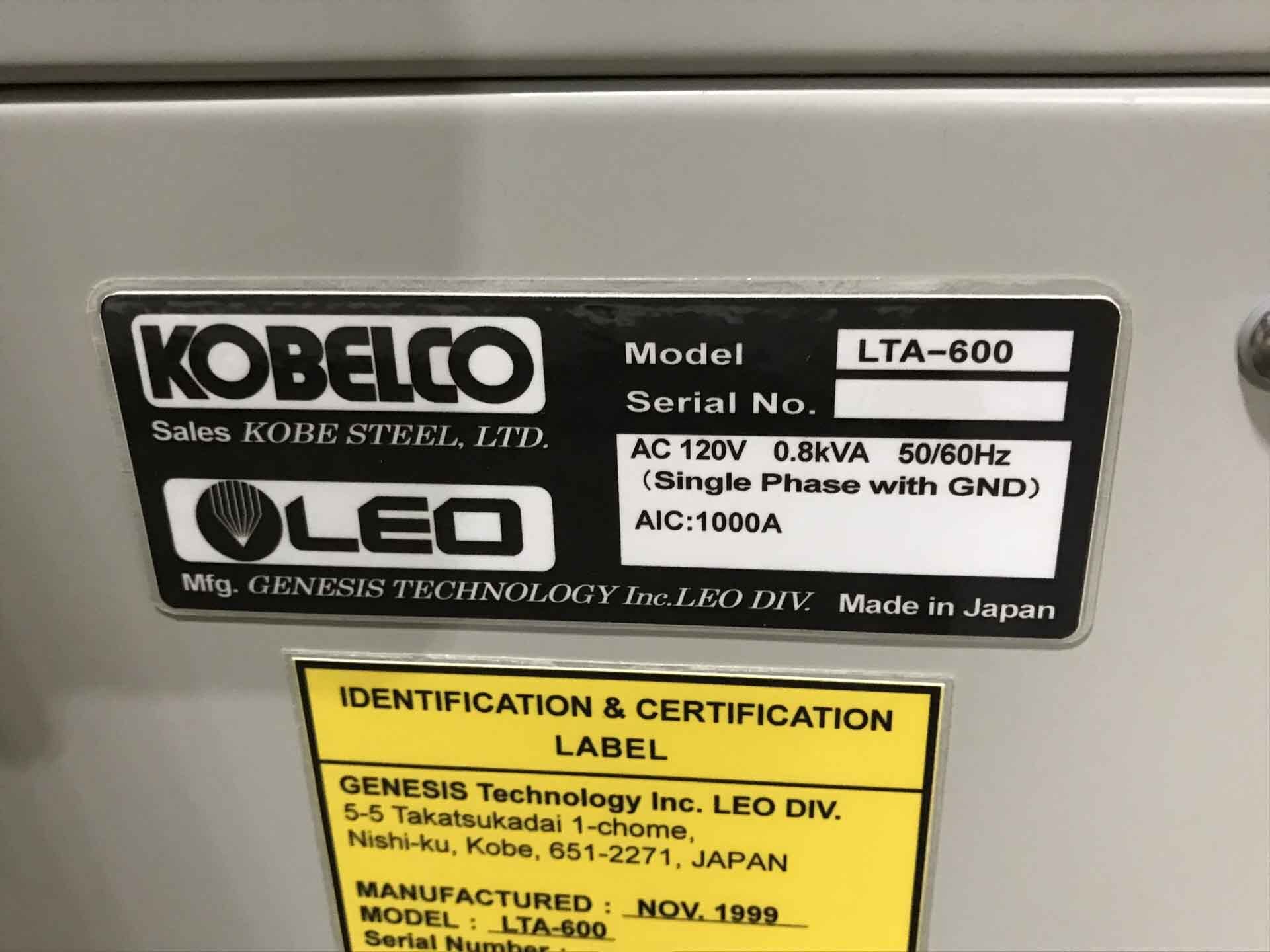
Vintage: 1999
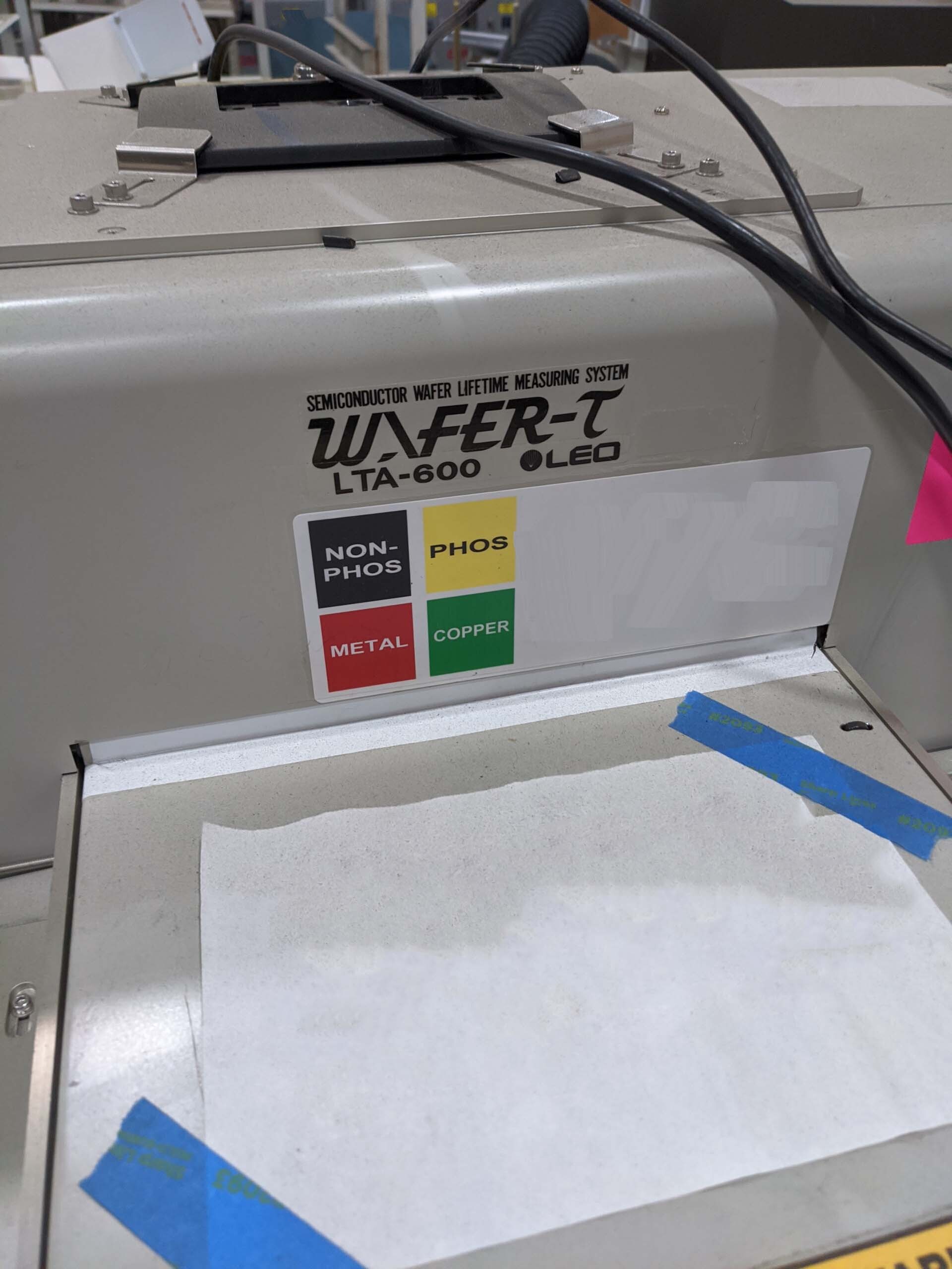
Lifetime measurement system, 8"
1999 vintage.
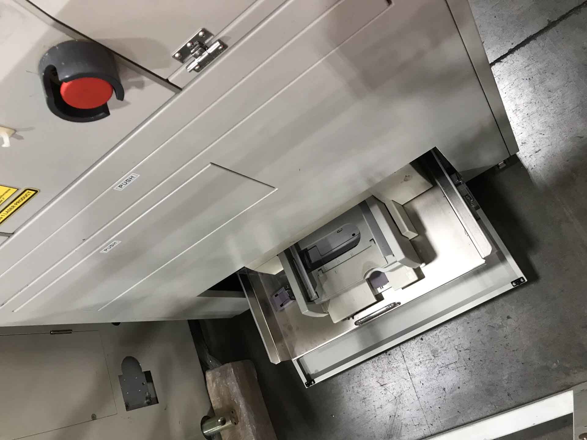
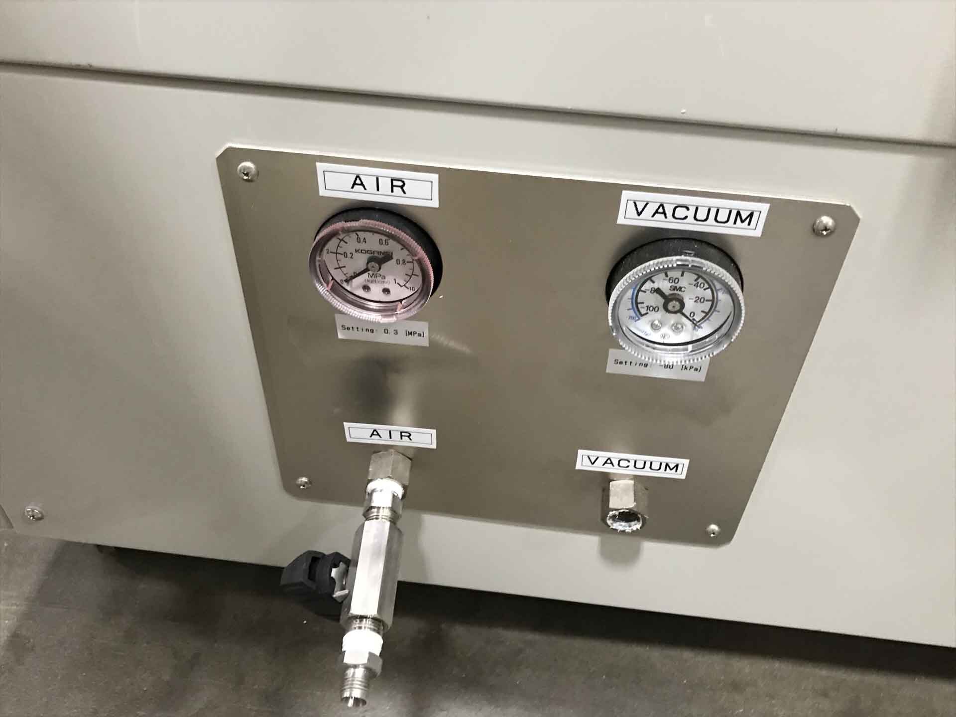
KOBELCO / LEO LTA-600 is an advanced wafer testing and metrology equipment designed to meet the stringent requirements of the semiconductor industry. This sophisticated equipment integrates cutting-edge technologies to provide comprehensive wafer inspection, measurement, and analysis capabilities. LEO LTA-600 is a versatile tool that enhances the efficiency and accuracy of wafer testing processes, contributing to the improvement of overall manufacturing quality and productivity. At the core of KOBELCO LTA-600 system is its precision wafer handling mechanism. This mechanism is engineered to securely hold and position wafers during the testing and measurement process, ensuring consistent and reliable results. The unit is capable of accommodating wafers of various sizes and materials, making it suitable for a wide range of semiconductor fabrication applications. LTA-600 machine features a state-of-the-art optical inspection module that enables high-resolution imaging of wafers. This module utilizes advanced imaging technologies, such as bright-field and dark-field microscopy, to capture detailed images of wafer surfaces. These images are then analyzed to detect and characterize defects, pattern deviations, and other anomalies that may affect the functionality of semiconductor devices. The tool's image processing algorithms are designed to accurately identify and classify defects, providing valuable insights into the quality of the wafers under inspection. In addition to optical inspection, KOBELCO / LEO LTA-600 asset is equipped with advanced metrology capabilities for precise measurement of critical parameters on wafers. The model can perform measurements of dimensions, thickness, roughness, and other key characteristics with high accuracy and repeatability. This metrology functionality allows semiconductor manufacturers to ensure that wafers meet the required specifications and standards, leading to improved product quality and reliability. LEO LTA-600 equipment is designed to streamline the wafer testing and metrology process through automation and integration. The system features advanced robotic handling systems that enable seamless wafer loading and unloading, reducing manual intervention and minimizing the risk of human error. The integration of multiple inspection and measurement modules into a single platform enhances operational efficiency and productivity, enabling semiconductor manufacturers to achieve faster turnaround times and higher throughput. Moreover, KOBELCO LTA-600 unit is equipped with sophisticated data management and analysis capabilities to support comprehensive process control and optimization. The machine can generate detailed reports and analytics based on the collected inspection and measurement data, providing valuable insights into process trends, defect patterns, and quality metrics. This data-driven approach enables semiconductor manufacturers to make informed decisions for process improvement and yield enhancement, ultimately leading to cost savings and competitive advantage in the industry. In conclusion, LTA-600 wafer testing and metrology tool represents a cutting-edge solution for semiconductor manufacturers seeking to achieve superior quality control, process efficiency, and productivity. With its advanced imaging, metrology, automation, and data analysis capabilities, KOBELCO / LEO LTA-600 asset is a reliable and versatile tool for optimizing wafer testing processes and ensuring the highest standards of semiconductor manufacturing.
There are no reviews yet