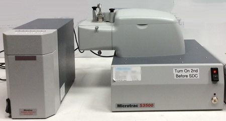
Used MICROTRAC S3500 #9215363 for sale
It looks like this item has already been sold. Check similar products below or contact us and our experienced team will find it for you.
Tap to zoom


Sold
ID: 9215363
Vintage: 2010
Micron particle counter system
With computer
Power cord
Tri-laser system
Particle size: 0.02 to 2800 microns
Standard range: Wet: 0.24 to 1400 um
Precision:
CV = 0.7% Spherical glass beads D50 = 642 micron
CV = 1.0% Spherical glass beads D50 = 56 micron
CV = 0.6% Spherical latex beads D50 = 0.4 micron
Lasers: Wavelength 780 nm
Power: 3 mW Nominal
Detection system: (2) Fixed photo-electric detectors
With logarithmically spaced segments
Optimal scattered light detection
0.02-163 Degrees using (151) detector segments
Data handling:
Data storing format: ODBC
Encryption: Microsoft access databases
Data integrity: FDA 21 CFR Part 11
Typical analysis time: 10 to 30 seconds
Environmental:
Temperature: 10 to 35°C
Humidity: 90% RH
Maximum storage temperature: -10° to 50° C
Pollution: Degree 2
Physical case: Steel and impact resistant plastic
Exterior surfaces: Corrosion resistant paint or plating
Dry operation: 100 psi (689 kPa)
Maximum pressure 5 CFM at 50 psi (345 kPa)
Minimum flow rate
Moisture / Oil
Vacuum: Exceed 50 CFM
Power:
AC Input: 90-132 VAC, 1 Phase, 47 to 63 Hz
200 to 265 VAC, 1 Phase, 47 63 Hz
Power consumption: 10 to 30 Seconds
2010 vintage.
MICROTRAC S3500 is a powerful and versatile wafer testing and metrology equipment for the semiconductor industry. It is designed for high-speed full-wafer measurements of spot, line and frame scans on wafers from 2" to 8". The system utilizes advanced optical technology combined with sophisticated image processing for enhanced measurements. MICROTRAC S 3500 features a large variety of tools, including a wafer testing and metrology unit, defect inspection and review, and wafer process monitoring. The main focus of S3500 is in characterizing very specific electrical properties of standard and advanced substrates and materials, such as resistivity, mobility, and capacitance. Additionally, S 3500 can measure the surface and thickness of wafers as well as identify subtle defects and variations. The machine is able to generate accurate data on wafer quality as well as additional summaries such as principle components, clusters, and regressions. The advanced user interface has a wide range of customizable options for operators which allow complete customization of the tool. MICROTRAC S3500 also features diagnostic capability for quickly mapping out a wafer pattern or structure. This includes the ability to distinguish between two types of defects that may be found on a wafer. Additionally, the visualization options provide convenient imaging capabilities as well as the ability to compare maps from two different wafers in order to identify critical process differences. Finally, the asset provides automated measurement of the entire wafer using statistical process control algorithms to define and analyze process variations. In comparison to other available technologies, MICROTRAC S 3500 offers the highest throughput for wafer testing and metrology. The model's state-of-the-art optical technologies provide superior accuracy and the advanced image processing algorithms provide quick and accurate results. The equipment is easy to install, maintain, and configure, providing an affordable solution for any wafer testing and metrology needs.
There are no reviews yet