Used N&K 1512 #293755557 for sale
URL successfully copied!
Tap to zoom
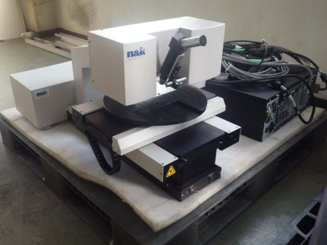

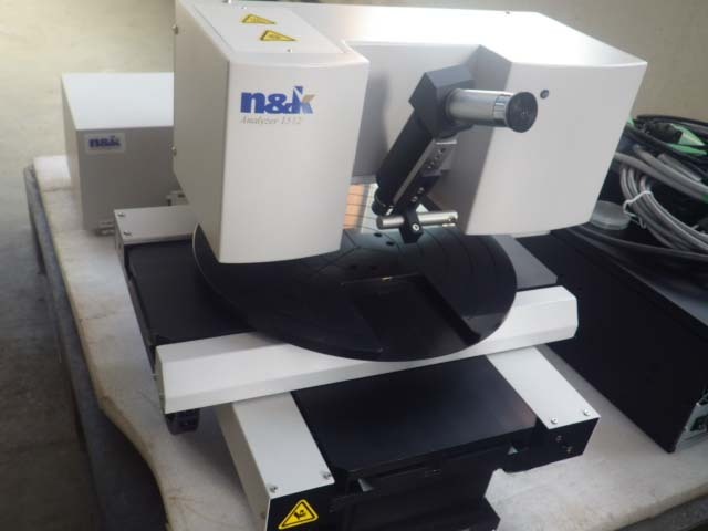
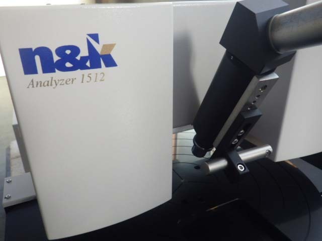
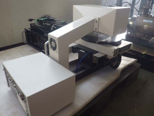
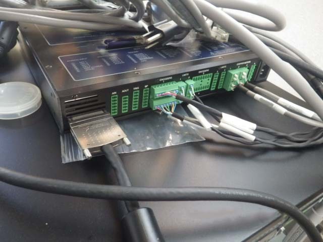
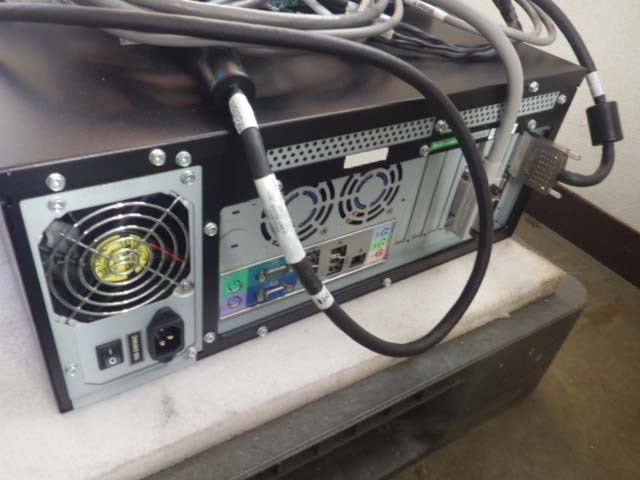
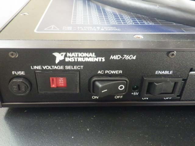
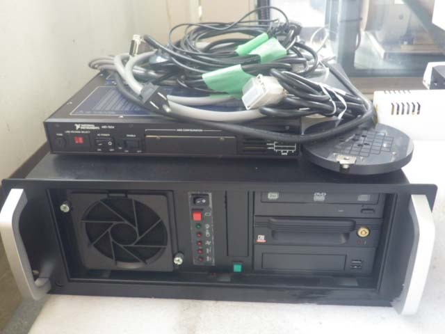
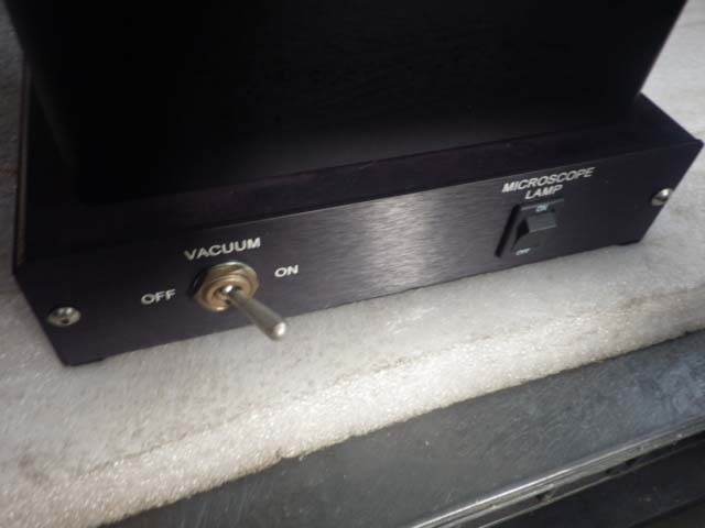
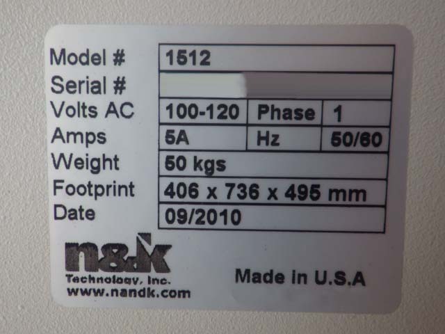
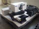
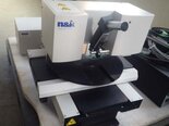
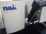
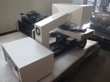
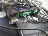
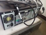
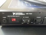
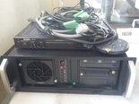
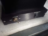
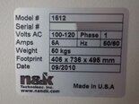
N&K 1512 is a precision wafer testing and metrology equipment, designed for measuring and analyzing a wide range of semiconductor wafers and thin films. The system is composed of a series of components that together provide comprehensive metrology capabilities in both laboratory and industrial applications. 1512 is made up of a two-axis staging unit that can be used to accurately and precisely position wafers in their desired location, along with a large, high-resolution imaging machine that provides the ability to photograph large surface areas of the wafers. This imaging tool is capable of detecting features as small as 5nm in size. The camera portion of the asset is capable of capturing both color optical and monochromatic polarized light images, allowing for a variety of different measurements to be made. In addition, it can be used to check for defects and uniformity on the wafer. The imaging components of the model are further supplemented with an AFM (Atomic Force Microscopy) module that can be used to measure the topography of the surface of the wafer, providing both the vertical and lateral feature sizes and shapes. N&K 1512 is also equipped with a spectroscopic module that is used to measure both thin film and wafer thickness as well as its index of refraction. It can measure thin film thicknesses down to 1 nanometer and refractive indices as low as 1.4. This equipment Analyser component of the system enables users to perform a variety of different measurements on the wafers, including sheet resistance, capacitance-capacitance, thickness, transmission, and resistivity measurements. The analyser component is complemented by an advanced software package that provides an intuitive interface for data entry and management, as well as a comprehensive graphical output for various testing and analysis procedures. Overall, 1512 provides a comprehensive testing and metrology solution for semiconductor wafers and thin films. The unit's comprehensive imaging capabilities, combined with its analyser component and software package, allows users to quickly and accurately measure a wide range of parameters on the wafers. This combination of components makes the machine ideal for both laboratory and industrial applications.
There are no reviews yet