Used NIKON 230565 #293756036 for sale
URL successfully copied!

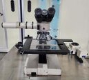
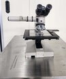
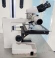
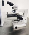
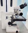
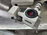
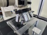
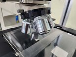
Tap to zoom
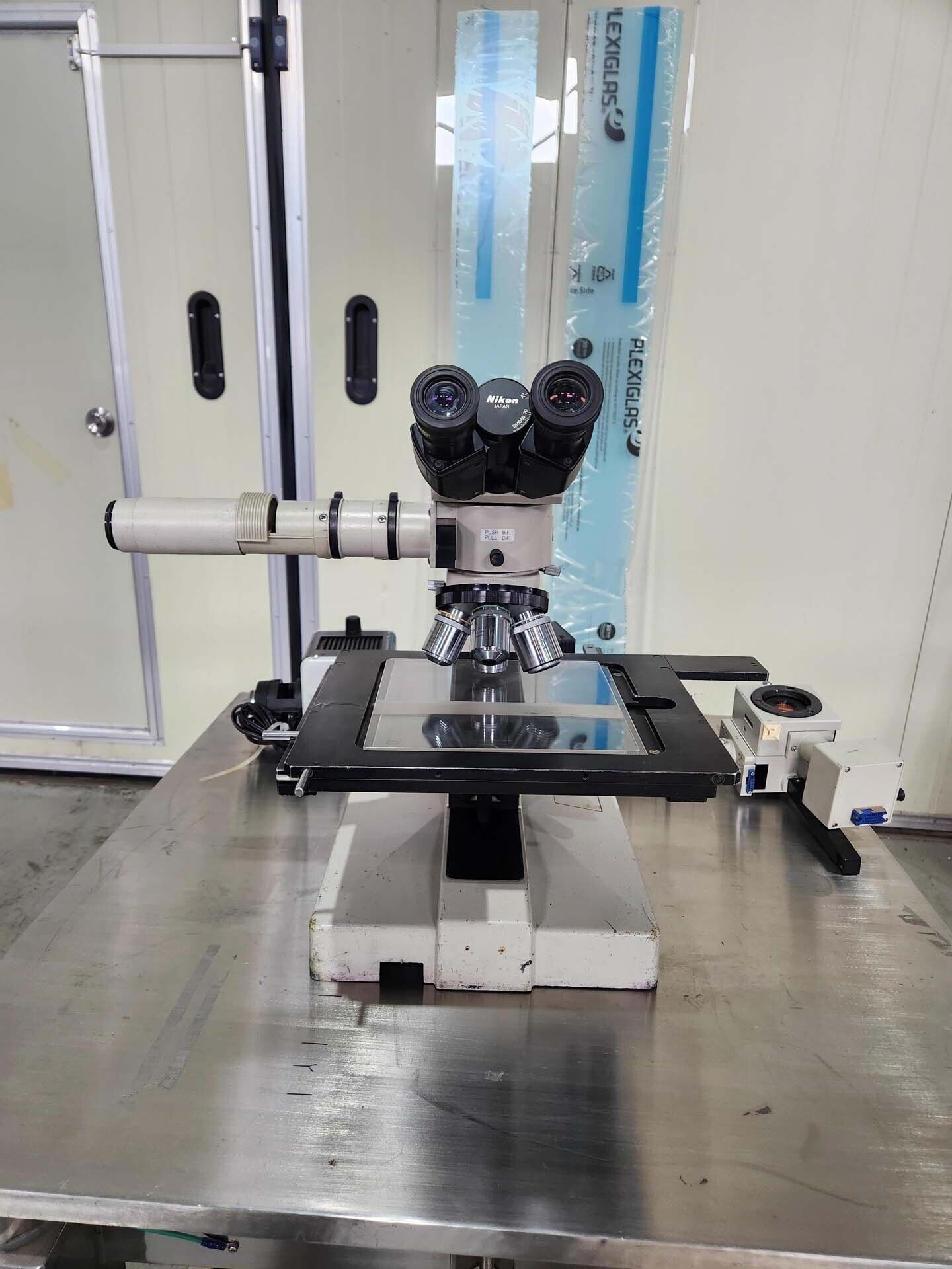

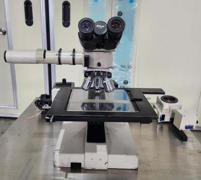
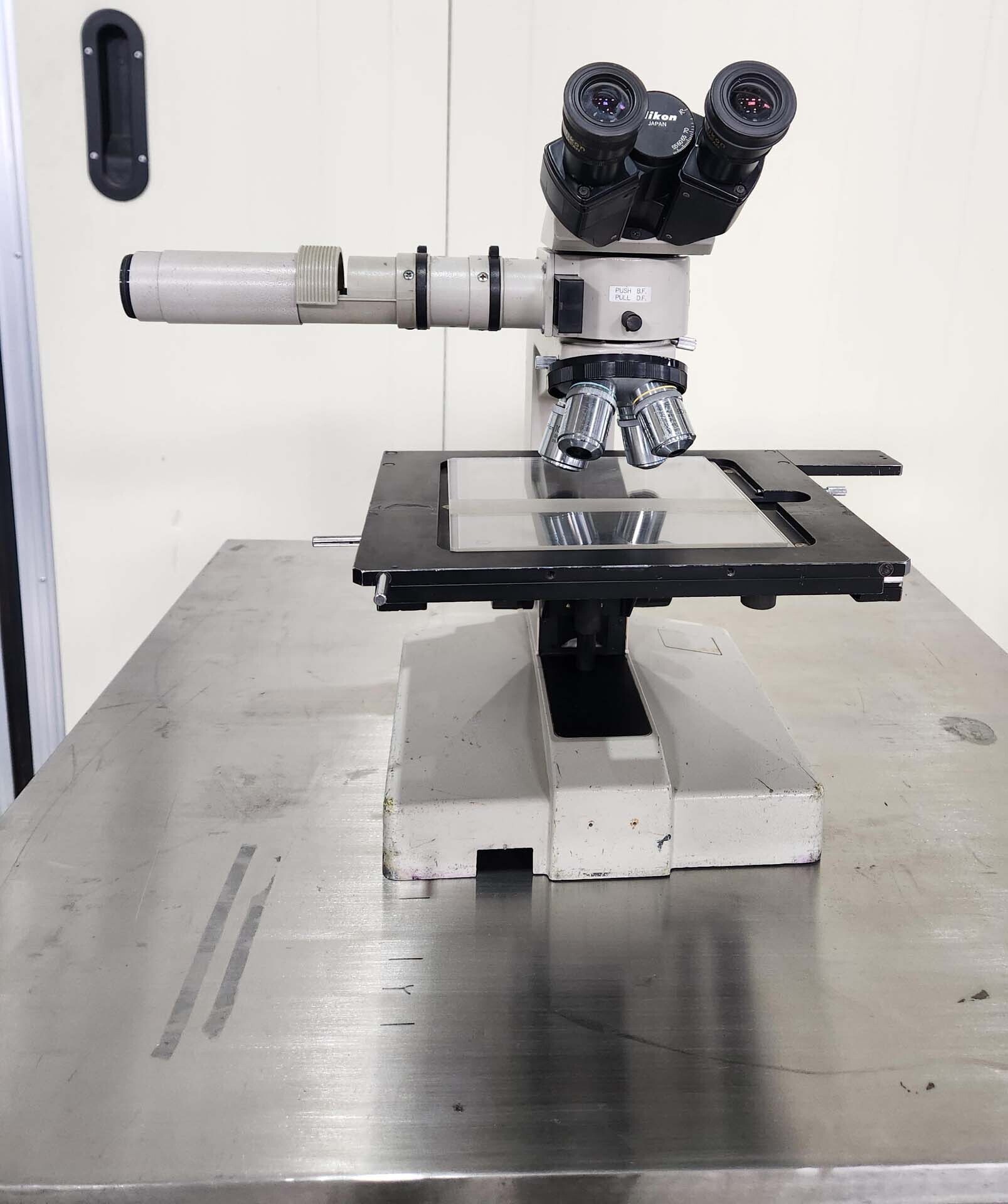
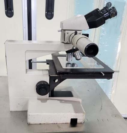
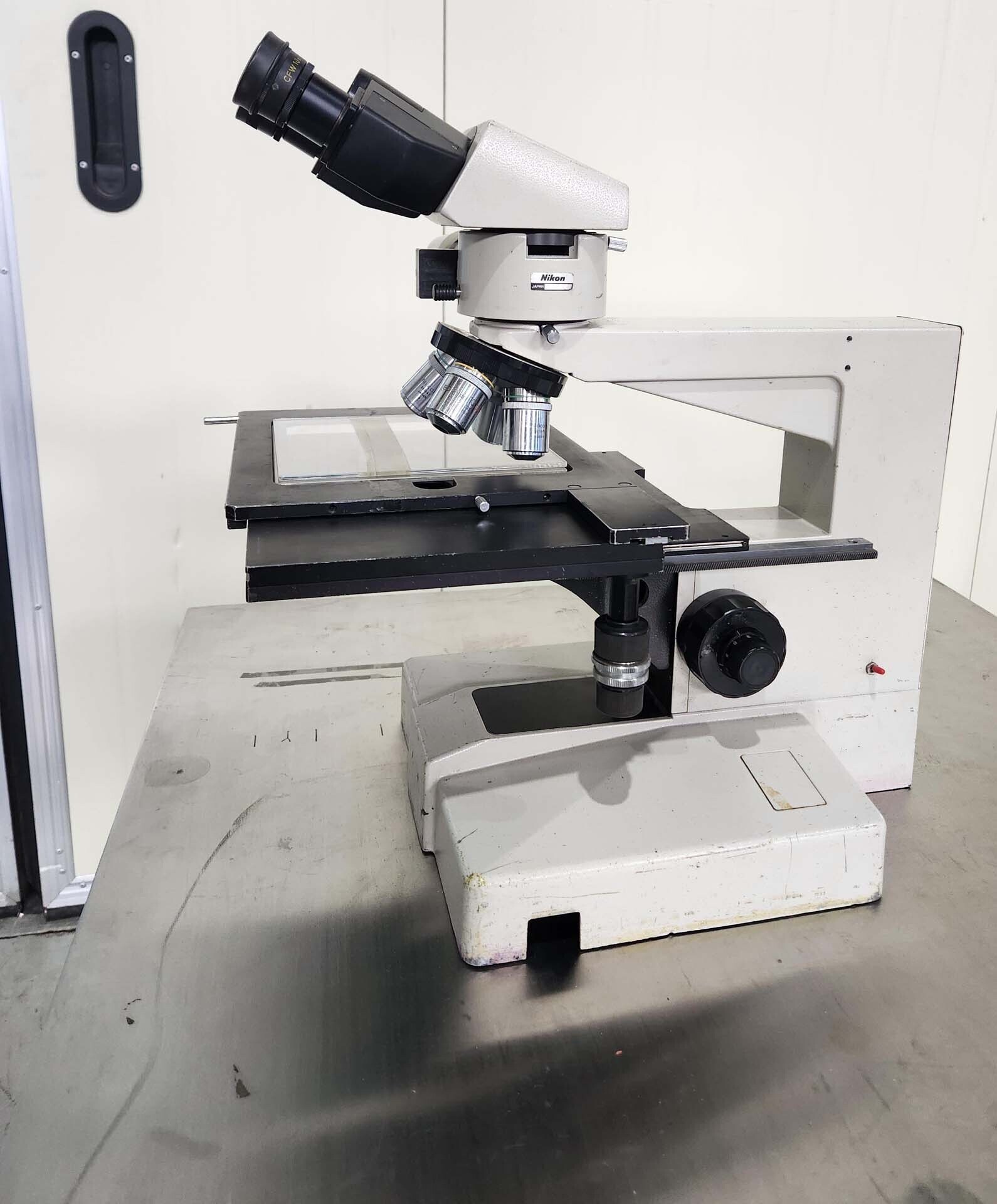
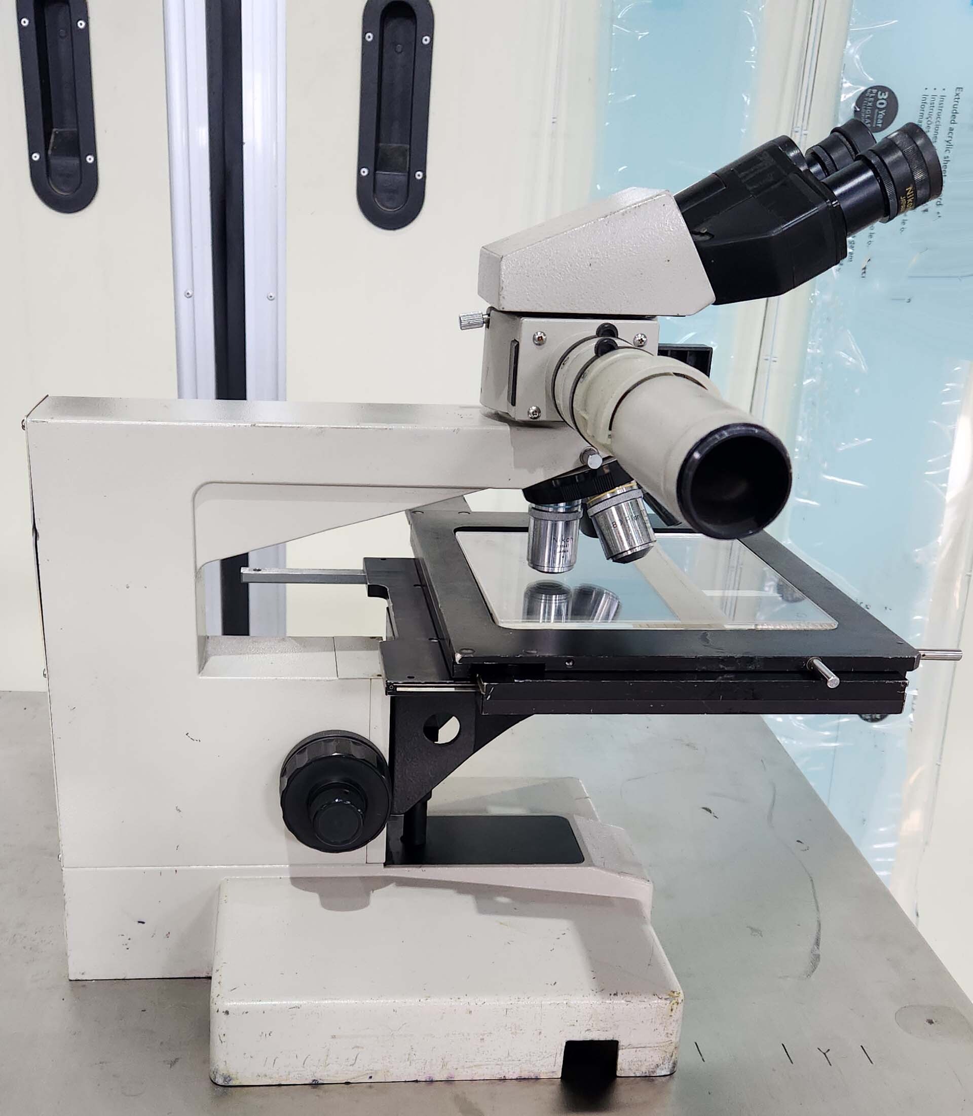
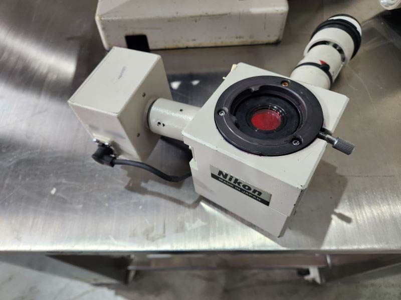
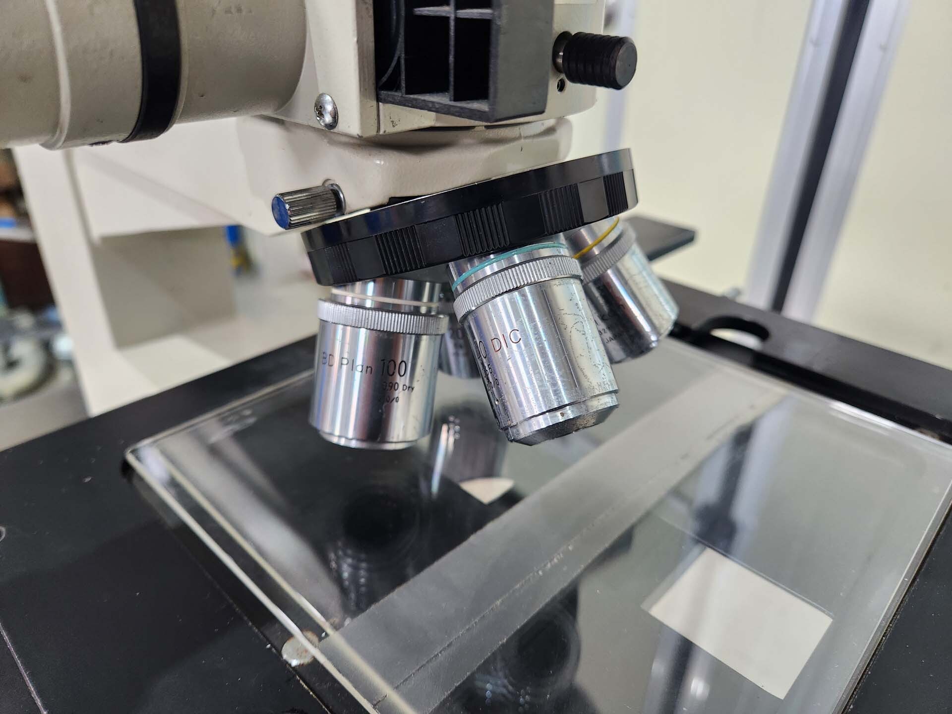
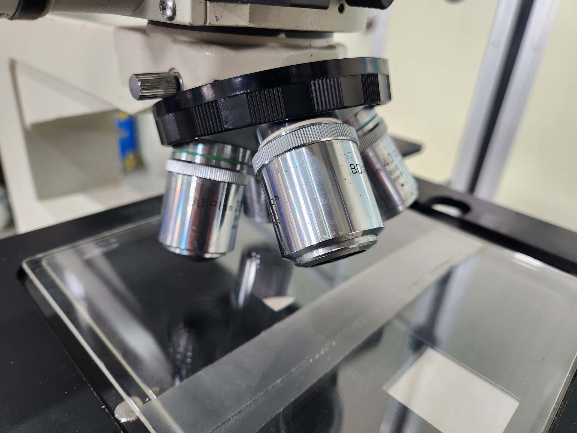
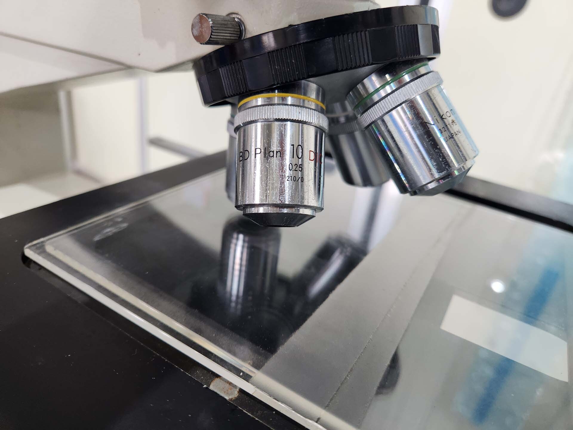
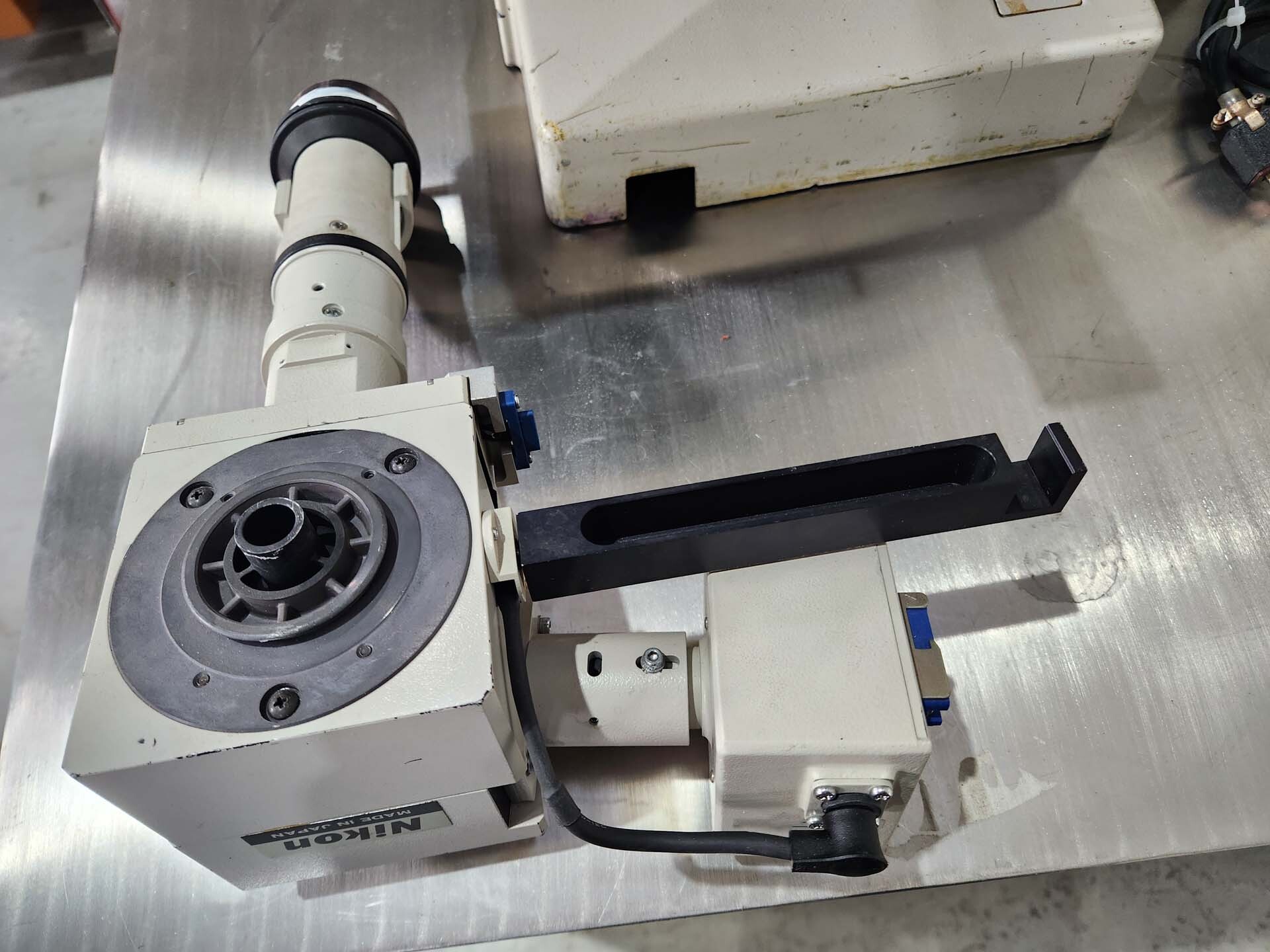
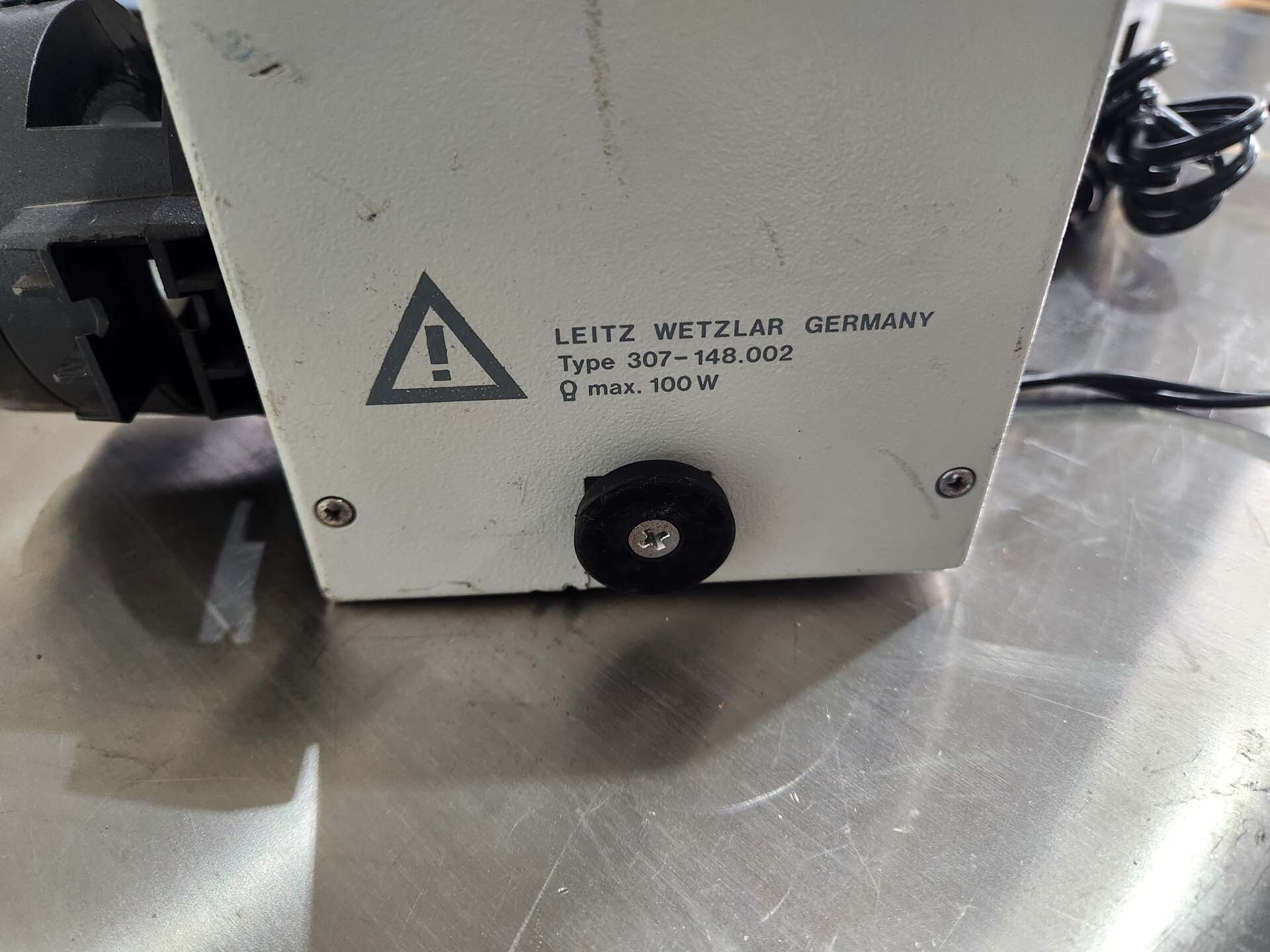
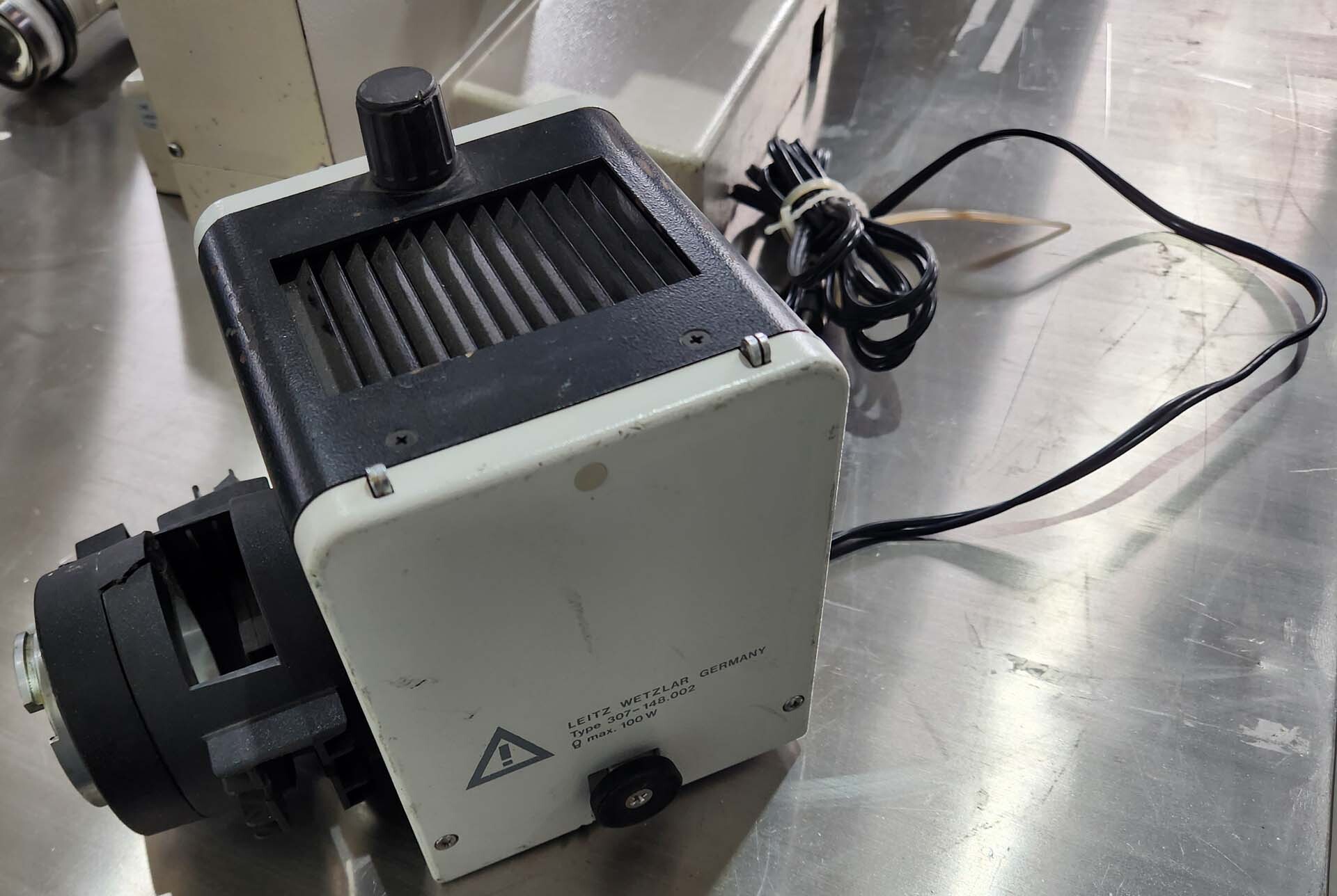
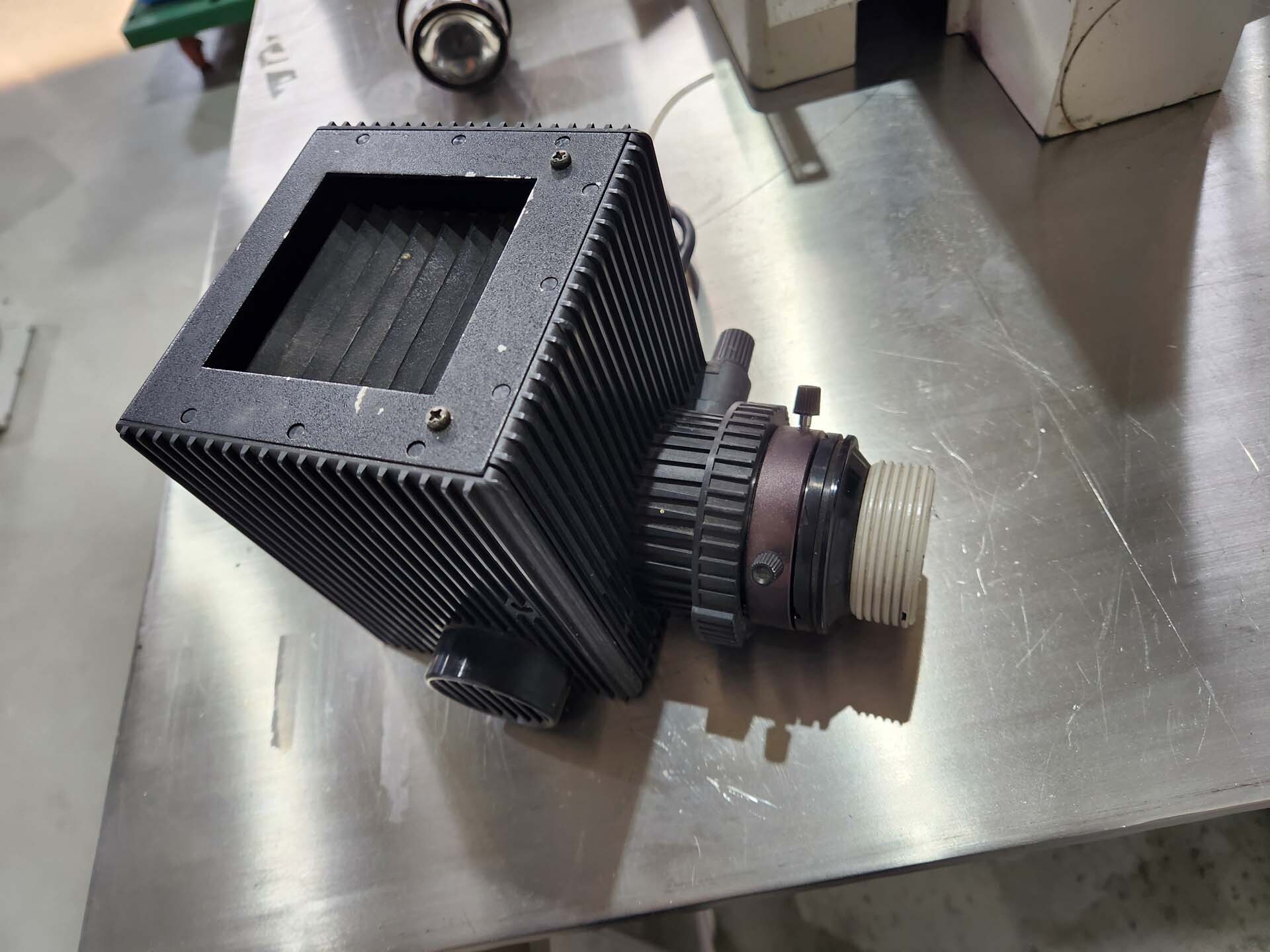
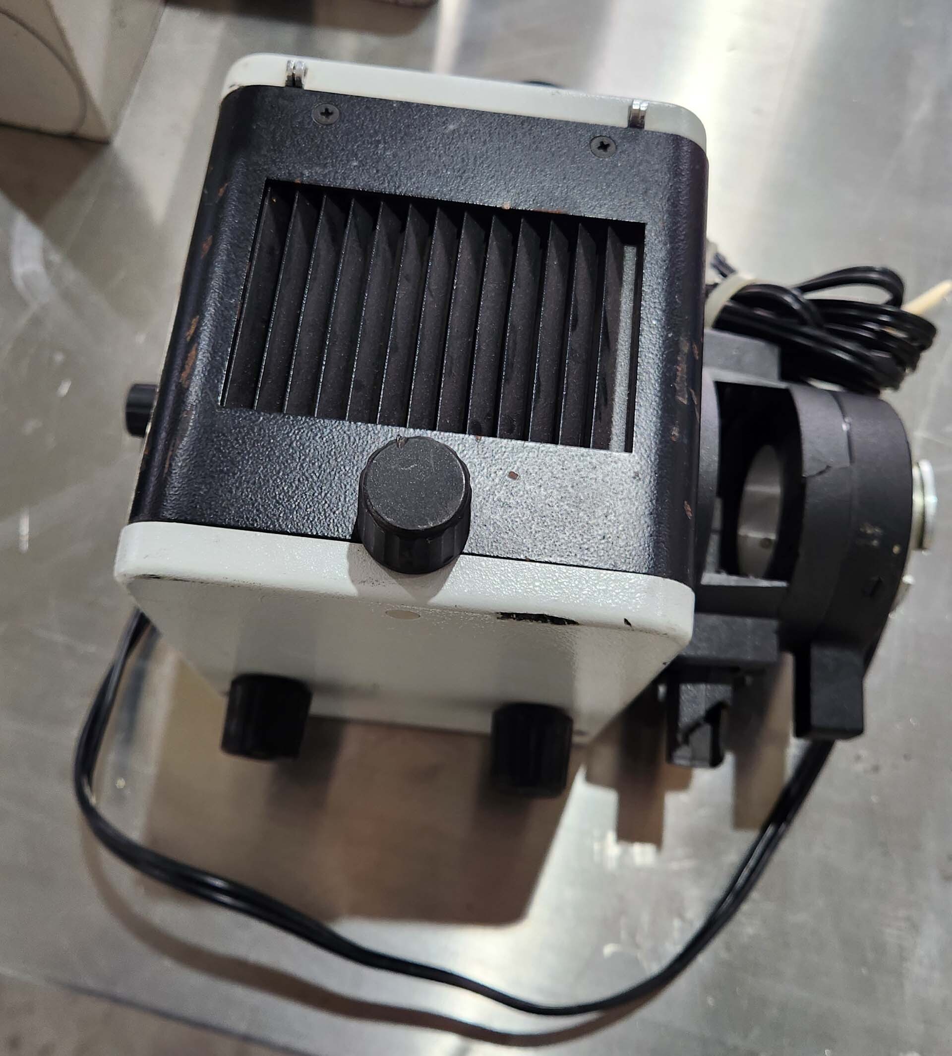
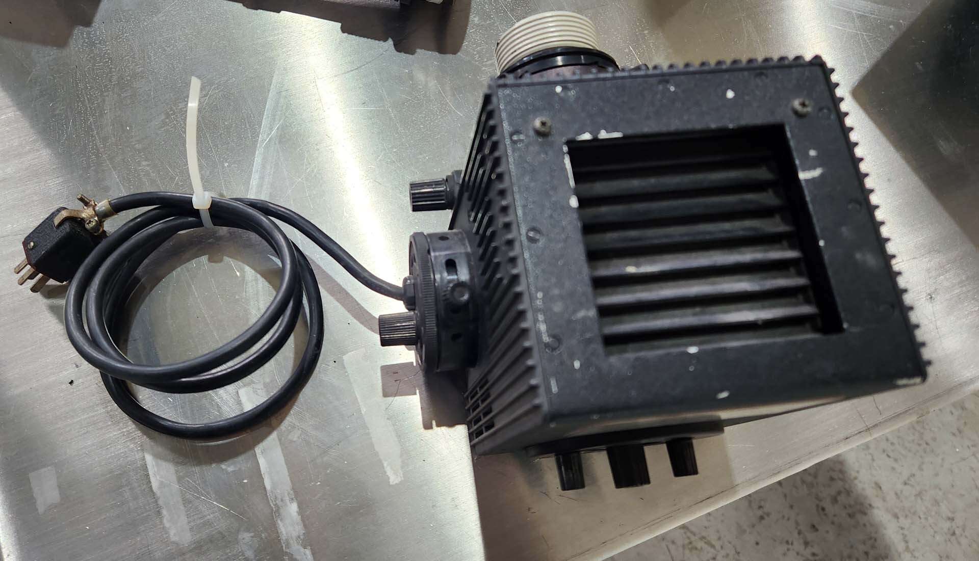
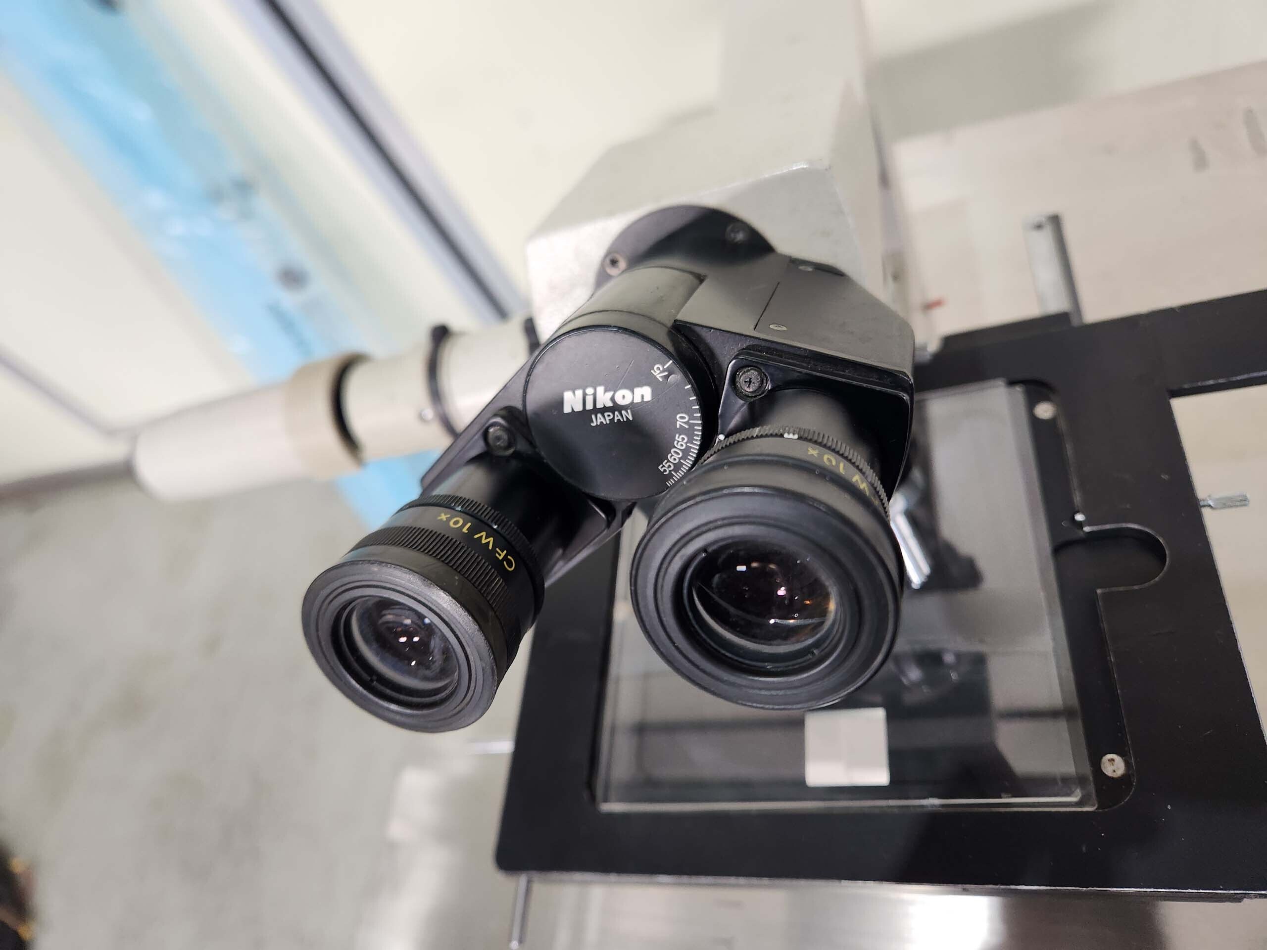
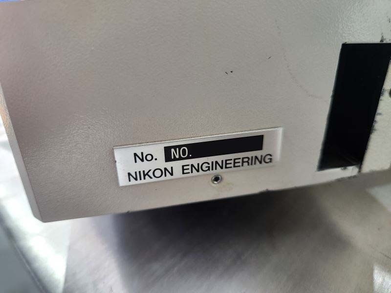
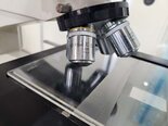
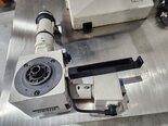
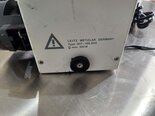
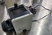
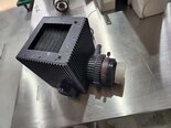
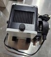
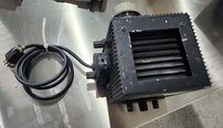
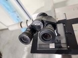
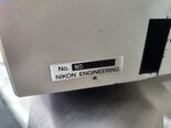
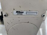
NIKON 230565 wafer testing and metrology equipment is a cutting-edge semiconductor manufacturing tool designed to optimize the quality control process for wafer fabrication. This system is equipped with advanced technology and features that enable accurate measurement, inspection, and analysis of semiconductor wafers to ensure their proper functionality and performance. At the core of 230565 unit is a high-resolution imaging machine that utilizes a combination of optical and digital imaging techniques to achieve precise and detailed imaging of the semiconductor wafers. The imaging tool is equipped with a high-quality CCD camera and advanced optics that allow for high magnification and resolution, enabling the asset to capture clear images of even the smallest features on the wafers. One of the key functionalities of NIKON 230565 model is wafer inspection, which involves the identification and analysis of defects or irregularities on the surface of the wafers. The equipment employs advanced algorithms and image processing techniques to automatically detect and categorize defects such as particles, scratches, and pattern deviations, allowing for quick and accurate identification of problematic areas on the wafers. In addition to wafer inspection, 230565 system also offers comprehensive metrology capabilities, enabling precise measurement and characterization of various parameters on the semiconductor wafers. The unit is equipped with specialized measurement tools and software algorithms that allow for accurate determination of critical dimensions, overlay accuracy, roughness, and other important parameters that affect the performance and functionality of the semiconductor devices fabricated on the wafers. NIKON 230565 wafer testing and metrology machine is designed for use in a cleanroom environment, ensuring that the wafers remain free from contamination during the testing and measurement process. The tool is designed with precision engineering and high-quality materials to maintain the integrity of the wafers and provide reliable and consistent results. One of the key advantages of 230565 asset is its user-friendly interface and intuitive software, which allow operators to easily set up tests, perform measurements, and analyze results with minimal training or expertise. The model also offers advanced data analysis and reporting capabilities, allowing users to generate detailed reports and visualizations of the test results for further analysis and decision-making. Overall, NIKON 230565 wafer testing and metrology equipment is a powerful and versatile tool for semiconductor manufacturers looking to enhance their quality control processes and improve the overall efficiency and reliability of their wafer fabrication operations. With its advanced imaging, inspection, and metrology capabilities, the system enables precise and accurate characterization of semiconductor wafers, helping manufacturers achieve higher yields and better-quality products in the competitive semiconductor market.
There are no reviews yet