Used NIKON 6D #293755339 for sale
URL successfully copied!
Tap to zoom
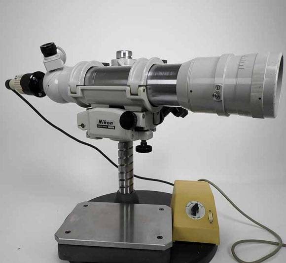

NIKON 6D is a cutting-edge wafer testing and metrology equipment that offers advanced capabilities for semiconductor manufacturing and research applications. This system is designed to meet the rigorous demands of the semiconductor industry by providing precise and accurate measurements of wafer characteristics and performance parameters. One of the key features of 6D unit is its high-precision optics, which enable detailed imaging and analysis of semiconductor wafers with sub-micron resolution. The machine is equipped with a sophisticated imaging sensor that captures high-resolution images of the wafer surface, allowing for precise measurements of critical dimensions, defect detection, and overlay alignment. In addition to its imaging capabilities, NIKON 6D tool is also equipped with advanced metrology tools for measuring various parameters of the wafer, such as film thickness, flatness, roughness, and critical dimensions. These metrology tools use advanced algorithms and algorithms to analyze the data collected from the wafer and provide detailed information about its quality and performance. 6D asset is designed to handle a wide range of wafer sizes and materials, making it suitable for use in the production of various semiconductor devices, including memory chips, logic chips, and power devices. The model can accommodate both standard silicon wafers and advanced materials such as III-V compounds and 2D materials, making it versatile and adaptable to the evolving needs of the semiconductor industry. Another key feature of NIKON 6D equipment is its automated data analysis and reporting capabilities. The system is equipped with powerful software that can process large amounts of data collected during wafer testing and metrology, allowing for rapid analysis and interpretation of results. The software can generate detailed reports and graphs that can be used for process optimization, quality control, and yield improvement. 6D unit is also designed with advanced automation features to streamline the wafer testing and metrology process. The machine can be integrated into a fully automated production line, allowing for high-throughput testing and metrology of wafers with minimal human intervention. This automation capability helps to improve efficiency, reduce errors, and increase overall productivity in semiconductor manufacturing facilities. Overall, NIKON 6D wafer testing and metrology tool is a state-of-the-art solution for semiconductor manufacturers and researchers looking to achieve unparalleled levels of precision, accuracy, and efficiency in wafer characterization and analysis. With its advanced imaging, metrology, and automation capabilities, this asset is poised to drive innovation and advancements in semiconductor technology for years to come.
There are no reviews yet