Used NOVA NovaScan 3090 Next #293745763 for sale
URL successfully copied!
Tap to zoom
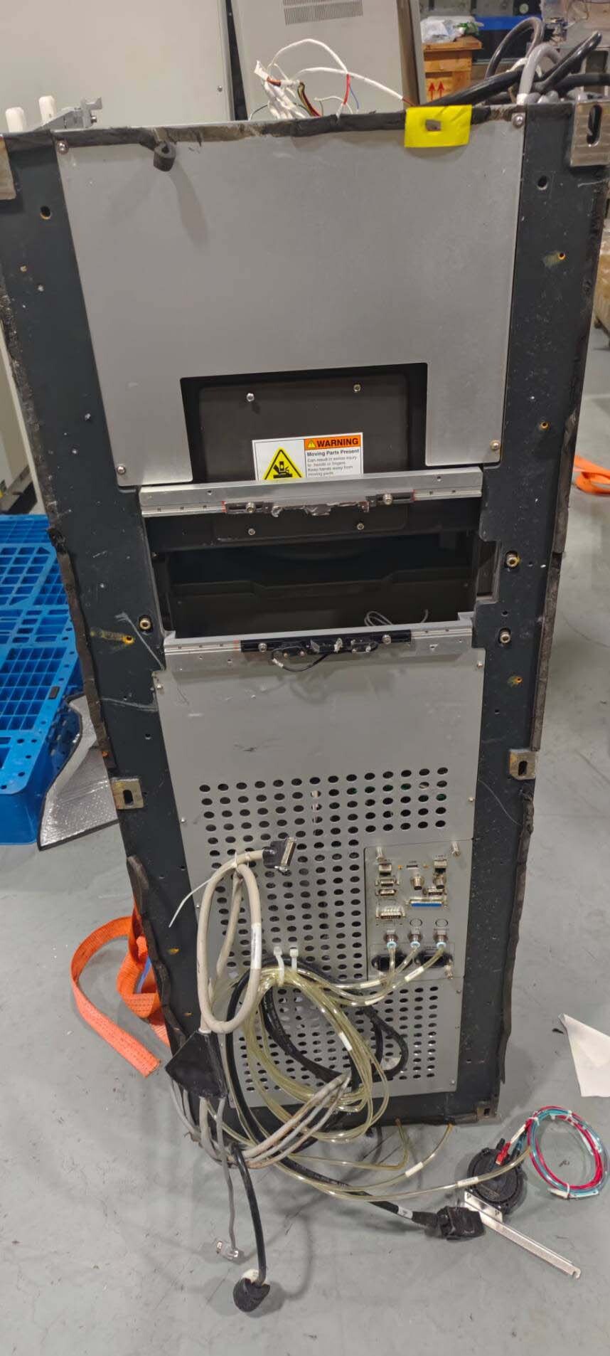

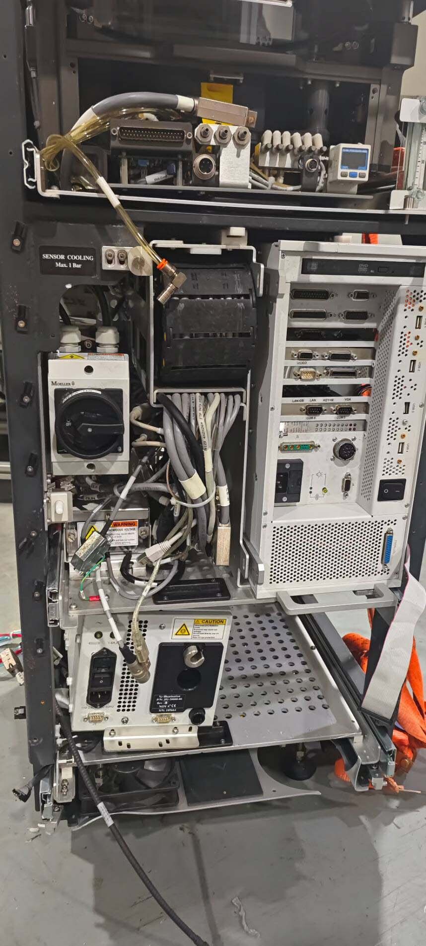
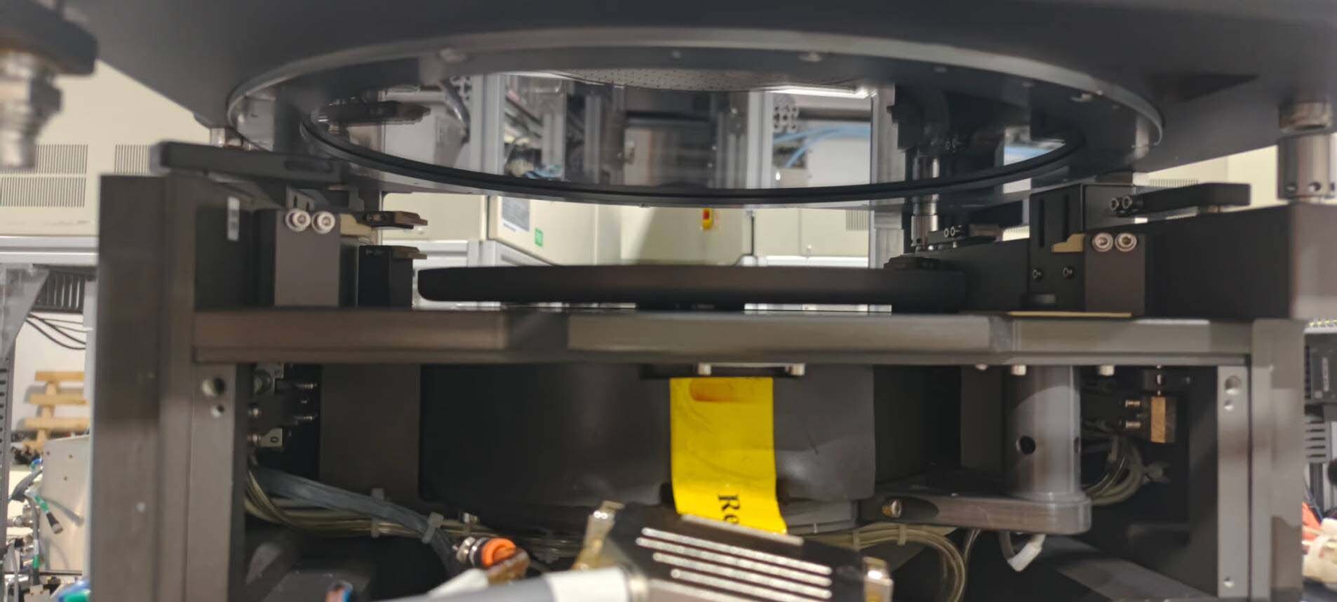
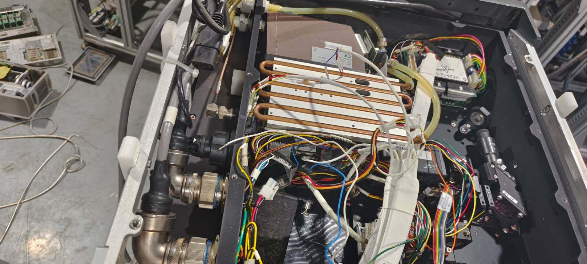
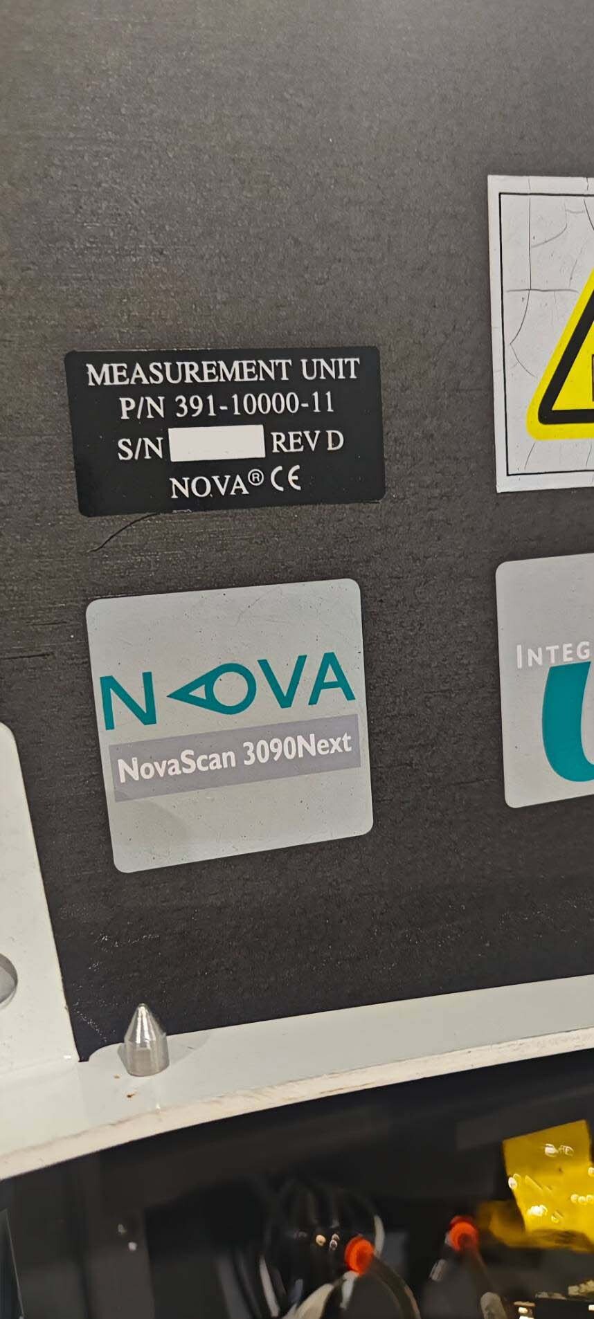
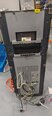
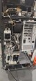
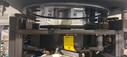
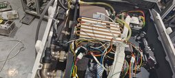
NOVA NovaScan 3090 Next is a cutting-edge wafer testing and metrology equipment designed to meet the demanding requirements of the semiconductor industry. This advanced system offers high-speed and accurate performance for the characterization and inspection of wafers used in the production of integrated circuits, memory devices, sensors, and other semiconductor applications. NovaScan 3090 Next is equipped with state-of-the-art technology and features to provide comprehensive analysis and reliable results for quality control and process optimization. One of the key features of NOVA NovaScan 3090 Next is its innovative scanning technology, which enables rapid and precise measurements of critical parameters on semiconductor wafers. The unit utilizes advanced optical and imaging techniques to capture high-resolution images of the wafer surface, allowing for the detection of defects, particles, and other anomalies. This real-time imaging capability is essential for identifying process variations and ensuring the quality and reliability of semiconductor devices. NovaScan 3090 Next is also equipped with automated wafer handling capabilities, allowing for efficient and continuous testing of multiple wafers in a production environment. The machine can accommodate wafers of various sizes and thicknesses, making it versatile and adaptable to different manufacturing processes. With its high throughput and low downtime, NOVA NovaScan 3090 Next is ideal for high-volume production facilities requiring fast and accurate wafer testing. In terms of metrology capabilities, NovaScan 3090 Next offers a wide range of measurement options for characterizing the physical and electrical properties of semiconductor wafers. The tool can perform critical dimension measurements, thickness mapping, film stress analysis, and defect review with high precision and repeatability. NOVA NovaScan 3090 Next also features advanced data analysis tools and software algorithms for extracting valuable insights from the measurement data, enabling engineers to make informed decisions and optimize process parameters. Furthermore, NovaScan 3090 Next is designed with user-friendly interfaces and intuitive software controls for easy operation and customization. The asset offers flexible configuration options and customizable measurement recipes to meet the specific requirements of different applications and devices. Users can easily set up test protocols, define measurement parameters, and analyze results in real-time using the integrated software platform of NOVA NovaScan 3090 Next. Overall, NovaScan 3090 Next represents a state-of-the-art solution for wafer testing and metrology in the semiconductor industry. With its cutting-edge technology, high-performance capabilities, and user-friendly design, the model is poised to enhance the efficiency, reliability, and quality of semiconductor manufacturing processes. Whether used for research and development or production testing, NOVA NovaScan 3090 Next offers a comprehensive and reliable solution for characterizing semiconductor wafers and ensuring the performance of advanced semiconductor devices.
There are no reviews yet