Used NOVA NovaScan 3090 Next #293778334 for sale
URL successfully copied!
Tap to zoom
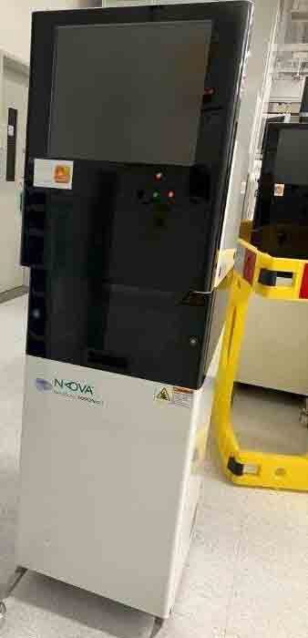

ID: 293778334
Wafer Size: 12"
Vintage: 2012
Critical Dimension (CD) measurement system, 12"
2012 vintage.
NOVA NovaScan 3090 Next is a cutting-edge wafer testing and metrology equipment designed to deliver high-precision inspection and measurement capabilities for semiconductor manufacturing processes. This advanced tool incorporates a range of innovative technologies to enable comprehensive analysis of wafer parameters with unprecedented accuracy and efficiency. The system is equipped with state-of-the-art sensors, imaging modules, and software algorithms to perform various critical functions, such as defect detection, overlay measurement, and film thickness analysis. One of the key features of NovaScan 3090 Next is its sophisticated defect detection capability. Using advanced imaging and scanning techniques, the unit can identify and classify defects on semiconductor wafers with exceptional sensitivity and resolution. This allows semiconductor manufacturers to quickly identify and address issues that could impact the quality and reliability of the final product. The machine's defect detection algorithms are highly customizable, enabling users to define specific criteria for different types of defects and optimize the inspection process for maximum efficiency. In addition to defect detection, NOVA NovaScan 3090 Next offers precise overlay measurement functionality. Overlay measurement is a critical aspect of semiconductor manufacturing, as it ensures the alignment and registration of different layers on the wafer. The tool utilizes advanced imaging techniques and software algorithms to accurately measure overlay errors and provide feedback for process optimization. With its high-resolution imaging capabilities and sophisticated metrology tools, NovaScan 3090 Next enables semiconductor manufacturers to achieve tighter overlay control and improve the overall yield of their production processes. Another key capability of NOVA NovaScan 3090 Next is its film thickness analysis feature. The asset uses a combination of optical and spectroscopic techniques to measure the thickness of various films deposited on the wafer surface. This information is crucial for ensuring uniformity and consistency in the manufacturing process, as variations in film thickness can lead to performance issues and defects in the final product. NovaScan 3090 Next provides accurate and reliable film thickness measurement capabilities, allowing manufacturers to monitor and control this critical parameter with precision. NOVA NovaScan 3090 Next is designed for seamless integration into semiconductor manufacturing environments, with a user-friendly interface and robust connectivity options. The model can be easily integrated with other tools and equipment in the production line, enabling streamlined data sharing and process control. Additionally, NovaScan 3090 Next is equipped with advanced data analysis and reporting capabilities, allowing users to generate detailed insights and statistics on wafer quality and process performance. Overall, NOVA NovaScan 3090 Next represents a significant advancement in wafer testing and metrology technology, offering semiconductor manufacturers a powerful tool for enhancing the quality, efficiency, and reliability of their production processes. With its advanced defect detection, overlay measurement, and film thickness analysis capabilities, this equipment enables manufacturers to achieve higher yields, faster time-to-market, and superior product quality in today's competitive semiconductor industry.
There are no reviews yet