Used RUDOLPH MP 200 #293749745 for sale
URL successfully copied!




Tap to zoom
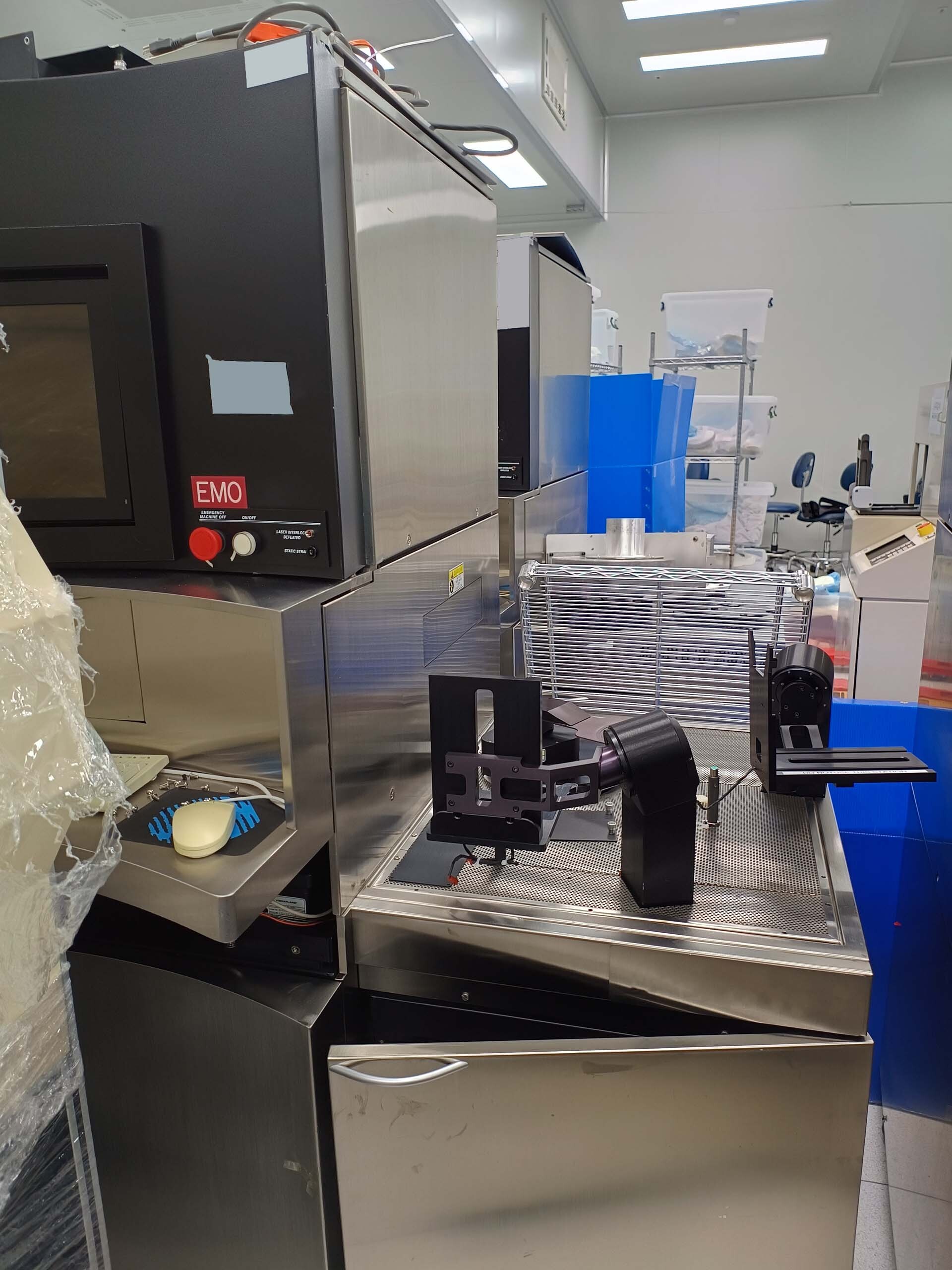

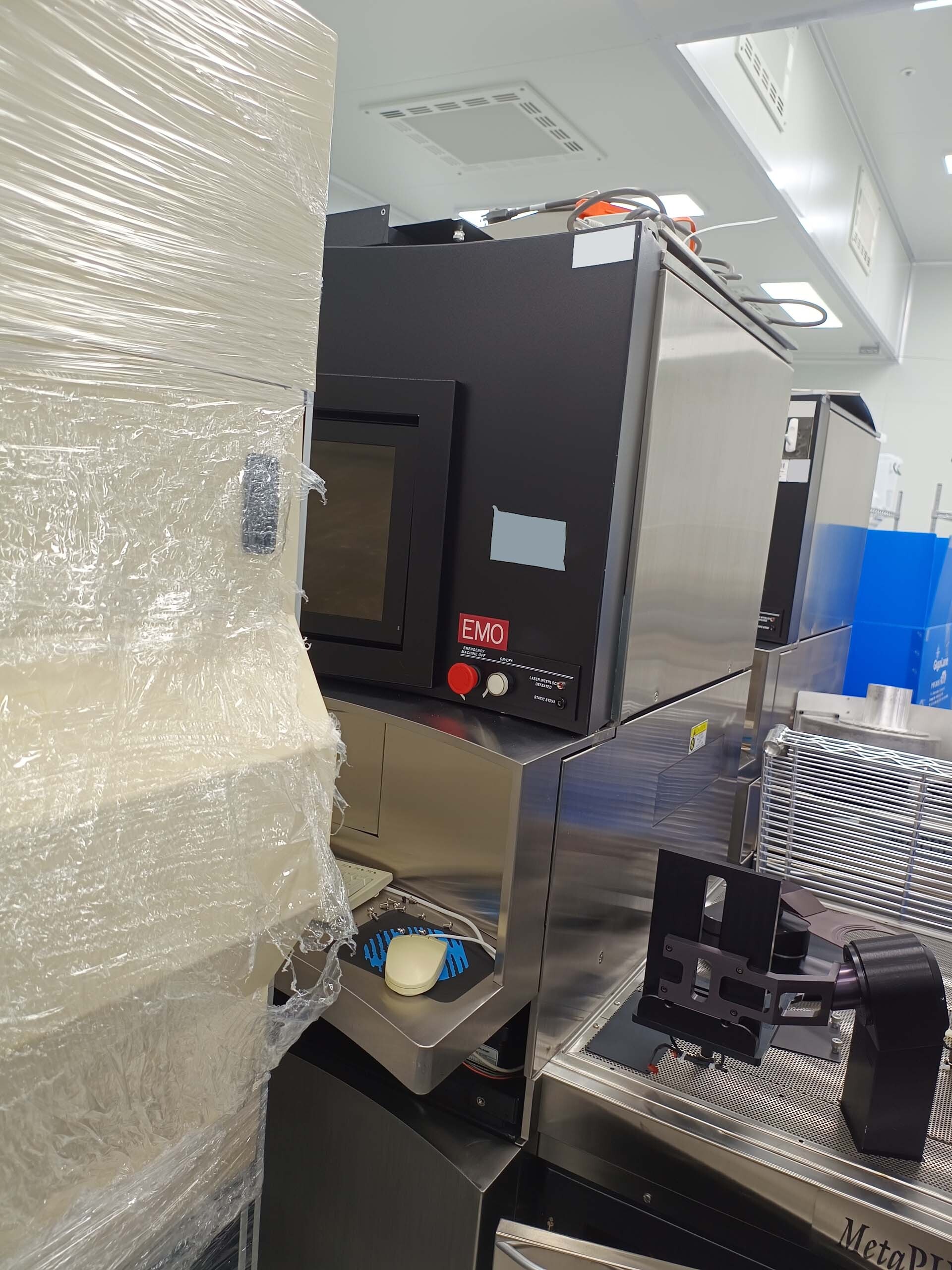
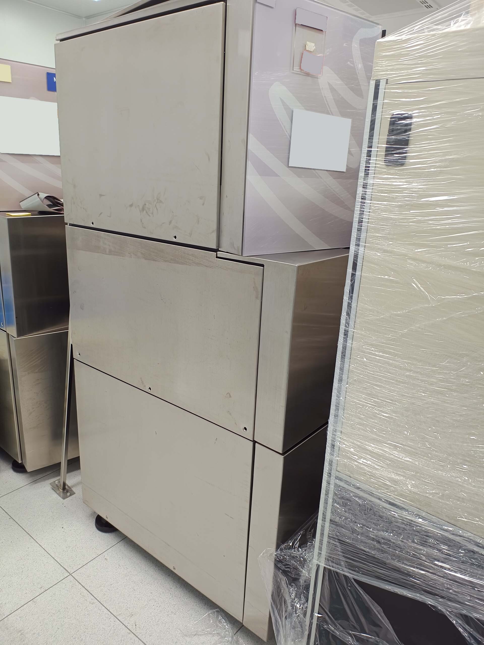
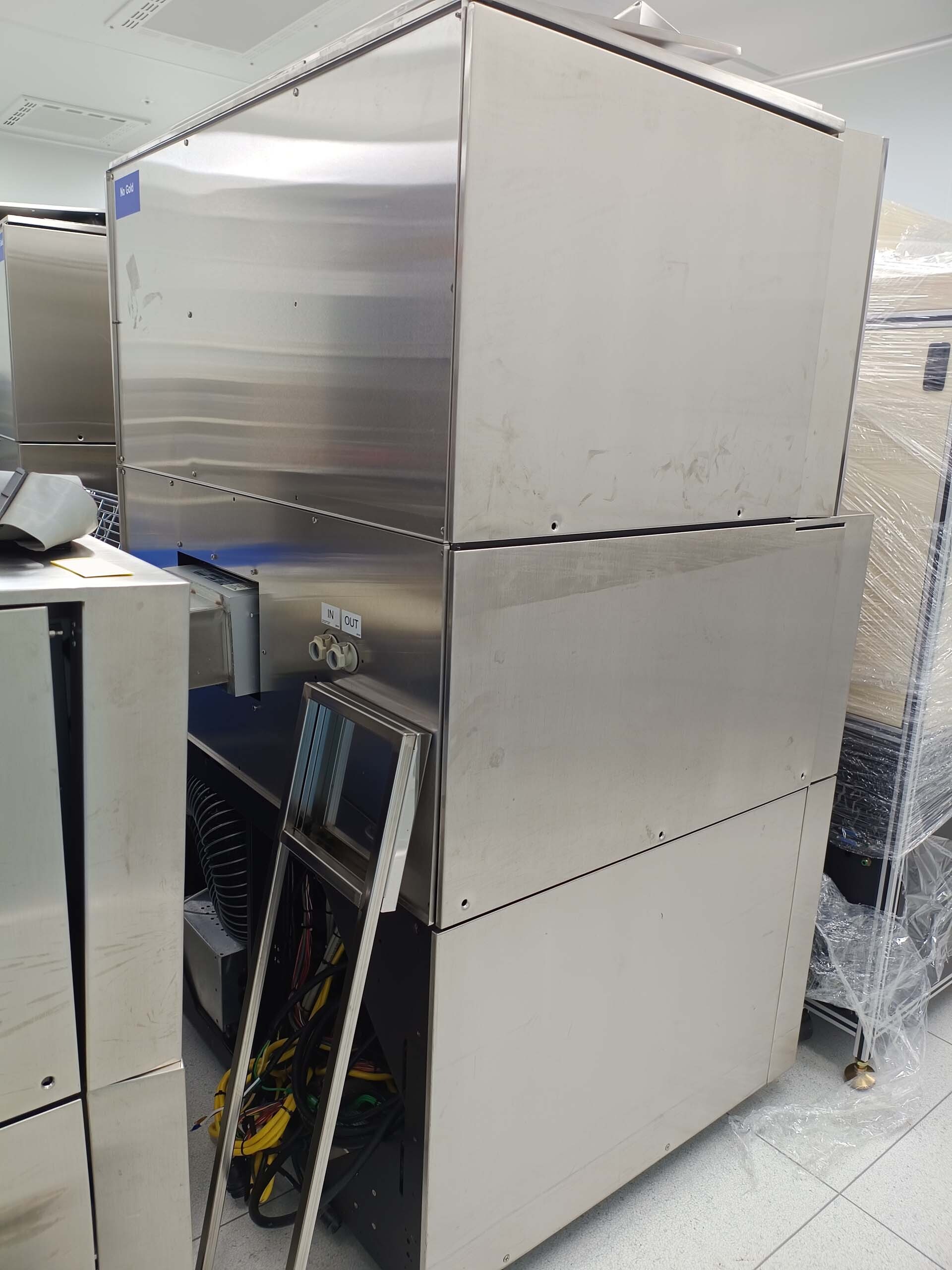
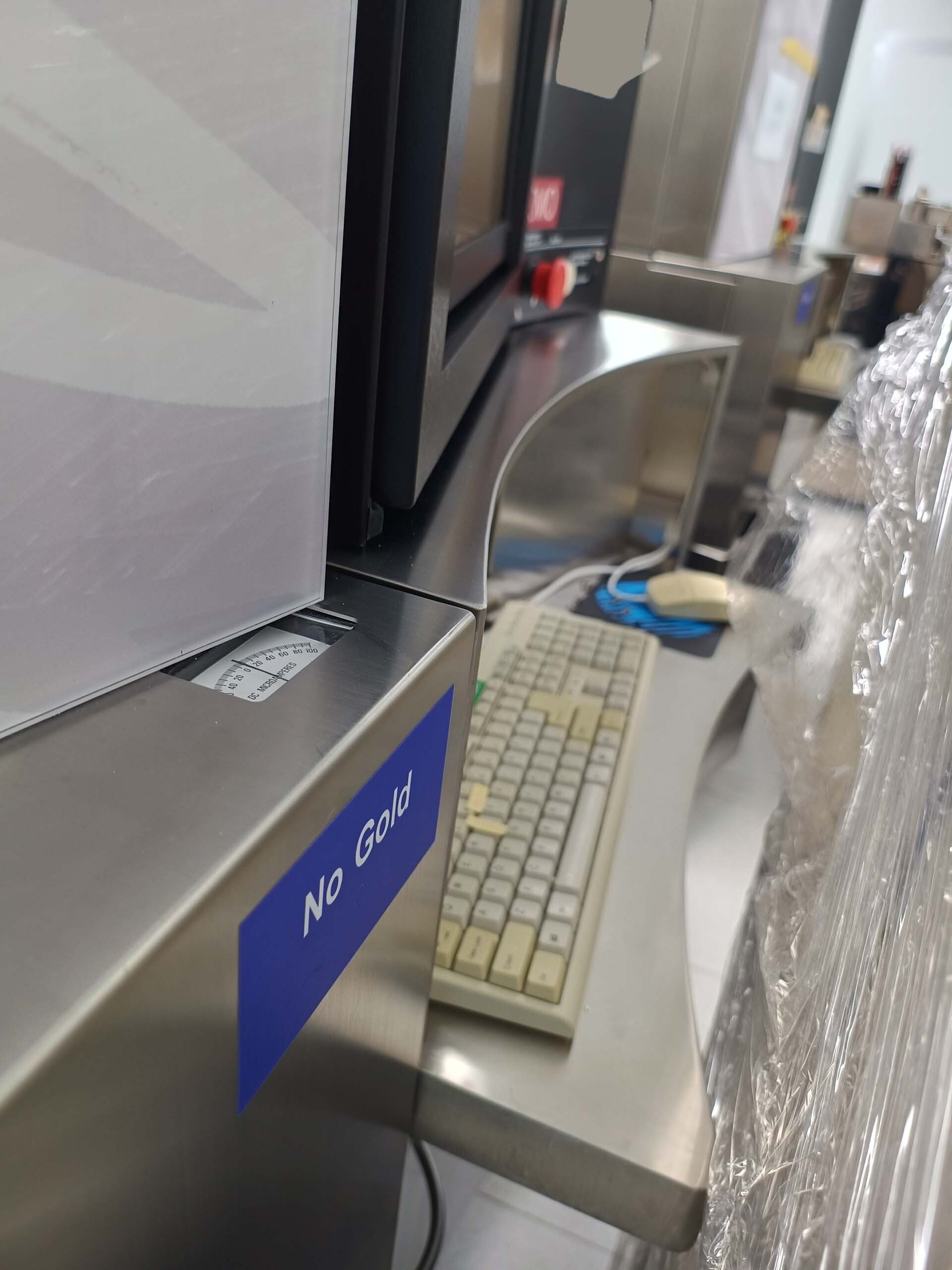
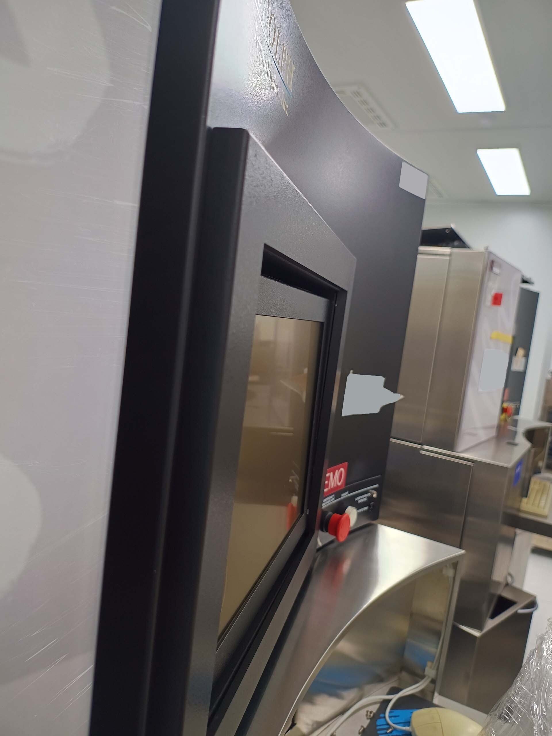
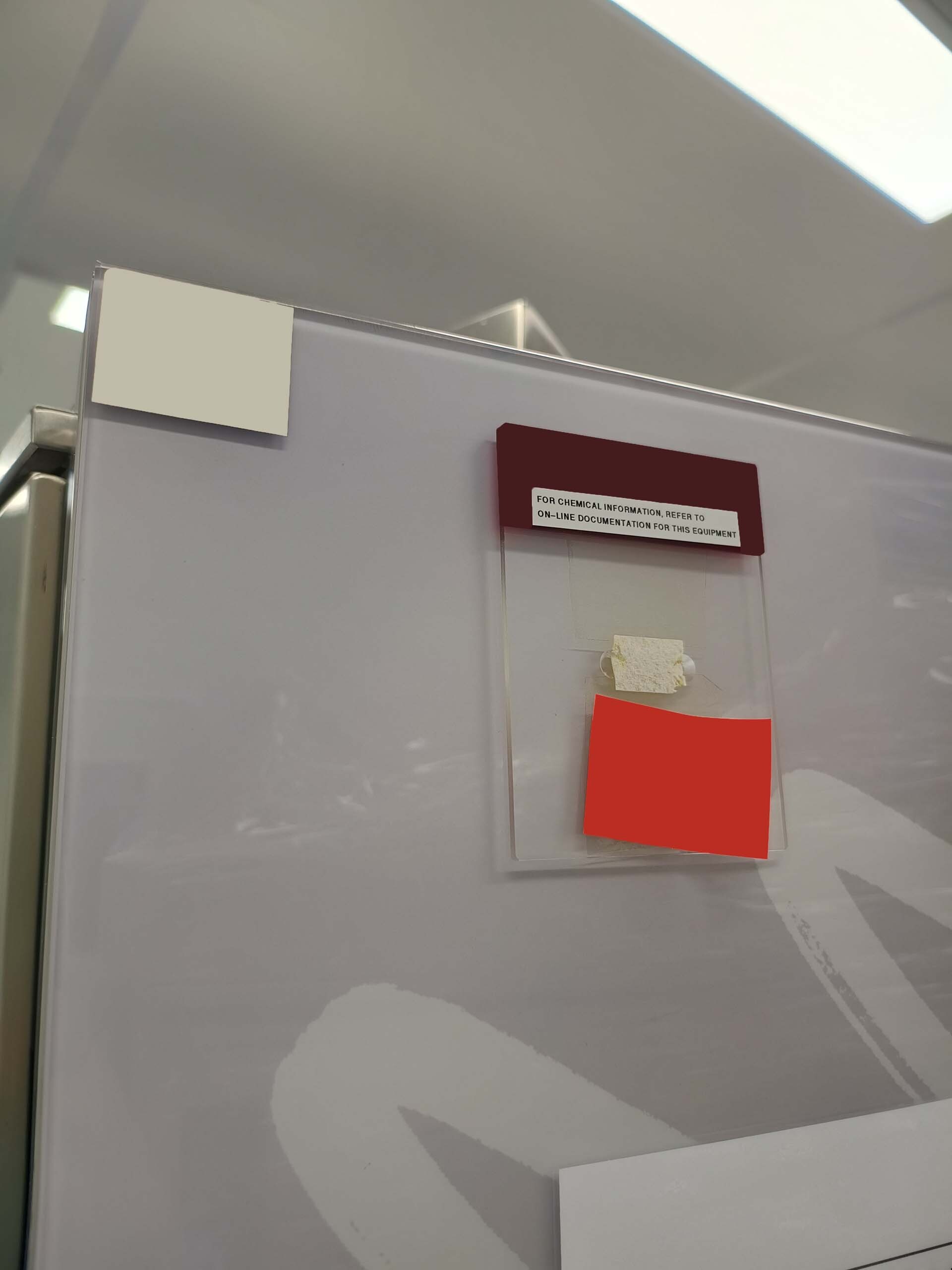
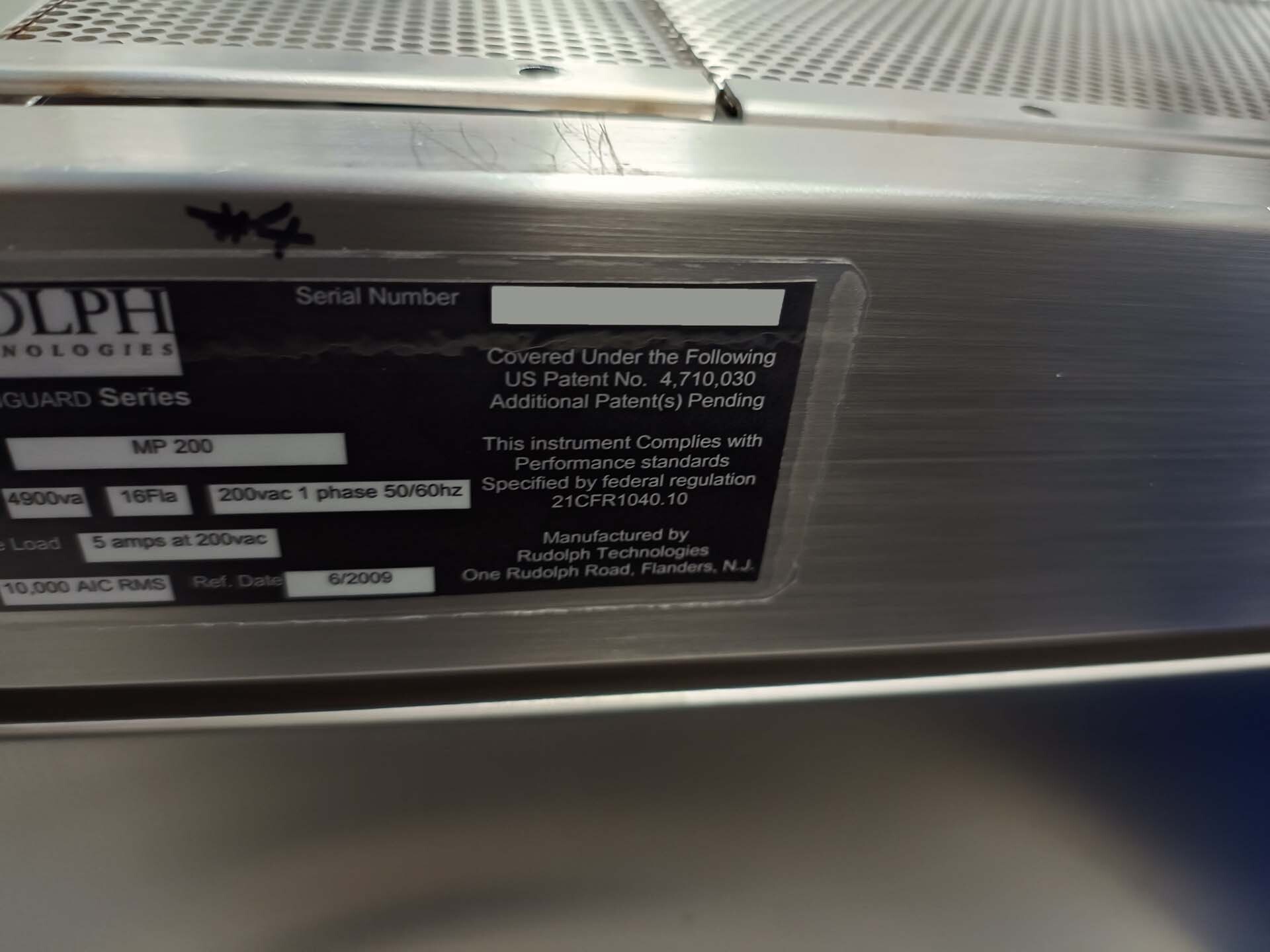
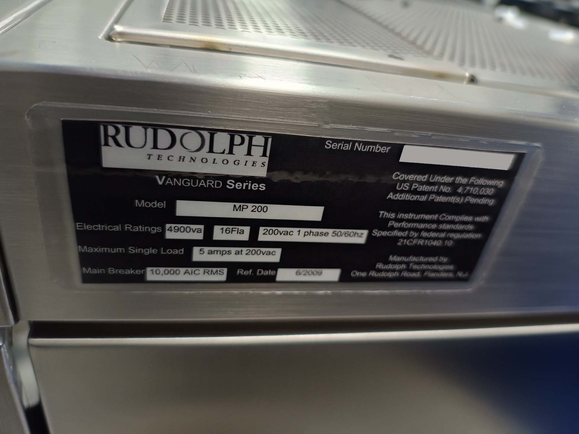
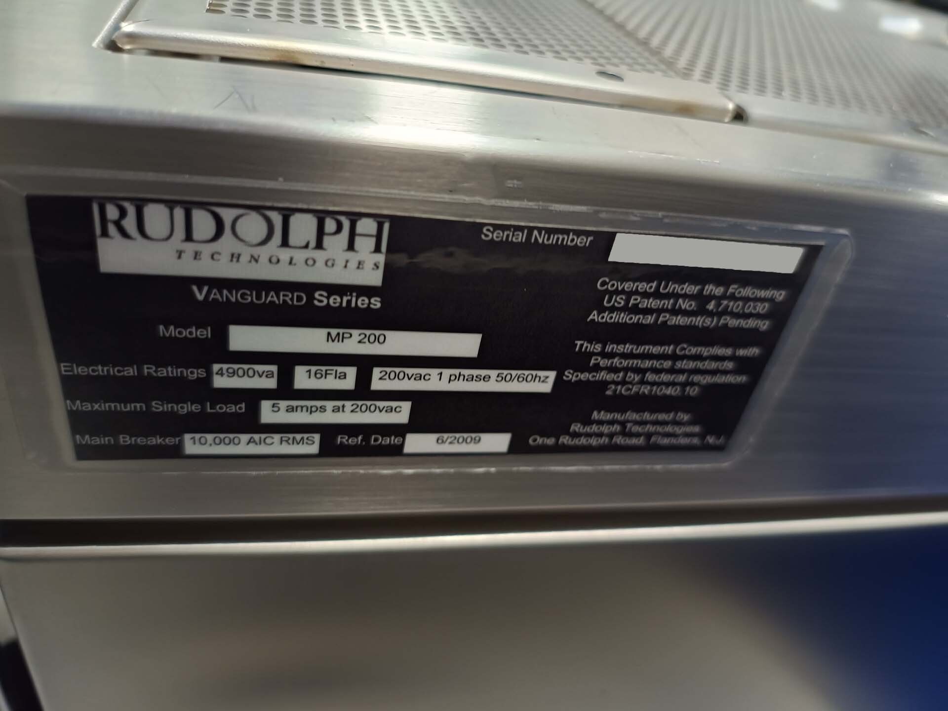
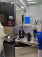
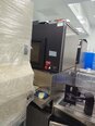
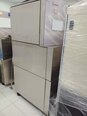
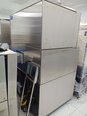
Wafer testing and metrology play a critical role in the semiconductor industry to ensure the quality and reliability of integrated circuits. RUDOLPH MP 200 is a state-of-the-art wafer testing and metrology equipment designed to provide accurate and efficient measurement solutions for semiconductor manufacturing processes. This advanced system offers a wide range of capabilities, including wafer mapping, defect inspection, film thickness measurement, and electrical testing, making it an essential tool for semiconductor manufacturers looking to improve their production yields and reduce time-to-market. MP 200 is equipped with a high-precision stage that allows for precise positioning of the wafer under test, ensuring accurate measurements and reliable results. The unit integrates advanced imaging and optical technologies, such as confocal microscopy and brightfield imaging, to capture high-resolution images of the wafer surface and detect defects with sub-micron resolution. This enables the machine to identify and classify defects accurately, helping manufacturers to troubleshoot fabrication issues and improve overall product quality. One of the key features of RUDOLPH MP 200 is its wafer mapping capability, which allows users to generate detailed maps of the wafer surface, including information on film thickness, roughness, and topography. This information is crucial for optimizing semiconductor manufacturing processes, as it helps to identify variations in film thickness and detect and locate defects that may impact device performance. The tool can perform rapid, automated wafer mapping with high throughput, making it an ideal solution for high-volume semiconductor production environments. In addition to wafer mapping, MP 200 offers comprehensive defect inspection capabilities, allowing users to detect and classify defects on the wafer surface accurately. The asset utilizes advanced algorithms and machine learning techniques to analyze images and identify different types of defects, such as particles, scratches, and cracks. By providing detailed information on defect size, shape, and location, the model enables manufacturers to identify root causes of defects and implement corrective actions to improve yield and reduce scrap. Moreover, RUDOLPH MP 200 is equipped with electrical testing functionality, enabling users to perform electrical characterization of semiconductor devices directly on the wafer. This feature is essential for verifying device functionality, measuring electrical properties, and identifying performance outliers that may indicate process deviations or material defects. By integrating electrical testing with other metrology capabilities, the equipment offers a holistic approach to semiconductor quality control, allowing manufacturers to assess both structural and electrical aspects of device performance. Overall, MP 200 is a versatile and powerful wafer testing and metrology system that offers advanced measurement solutions for semiconductor manufacturing applications. With its high accuracy, fast throughput, and comprehensive capabilities, the unit enables semiconductor manufacturers to achieve higher production yields, improve product quality, and accelerate time-to-market for cutting-edge semiconductor devices. By leveraging the capabilities of RUDOLPH MP 200, semiconductor manufacturers can stay competitive in the rapidly evolving semiconductor industry and meet the growing demands for reliable and high-performance integrated circuits.
There are no reviews yet