Used SEONBI SV-HPLU821 #293827917 for sale
URL successfully copied!

Tap to zoom
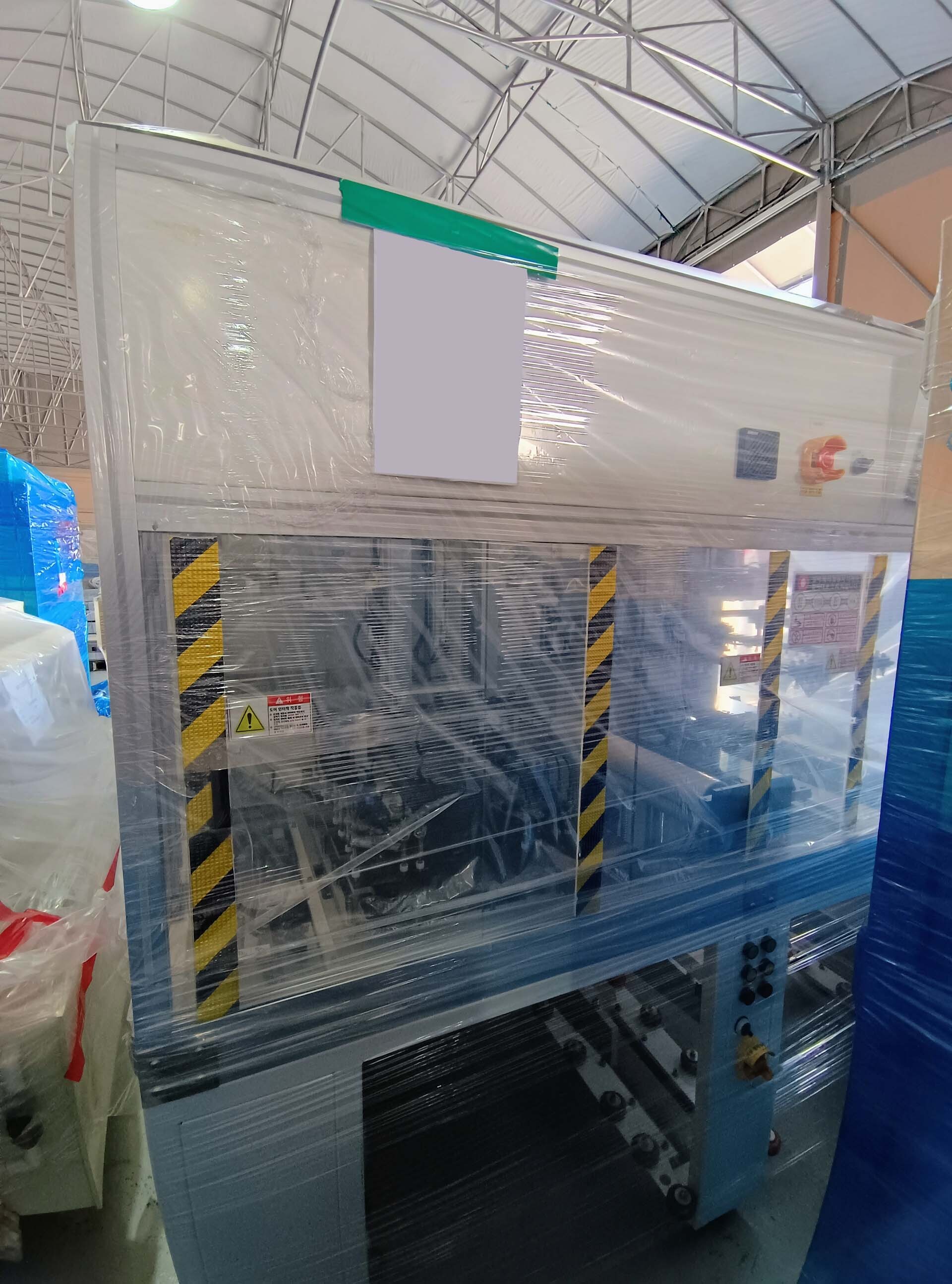

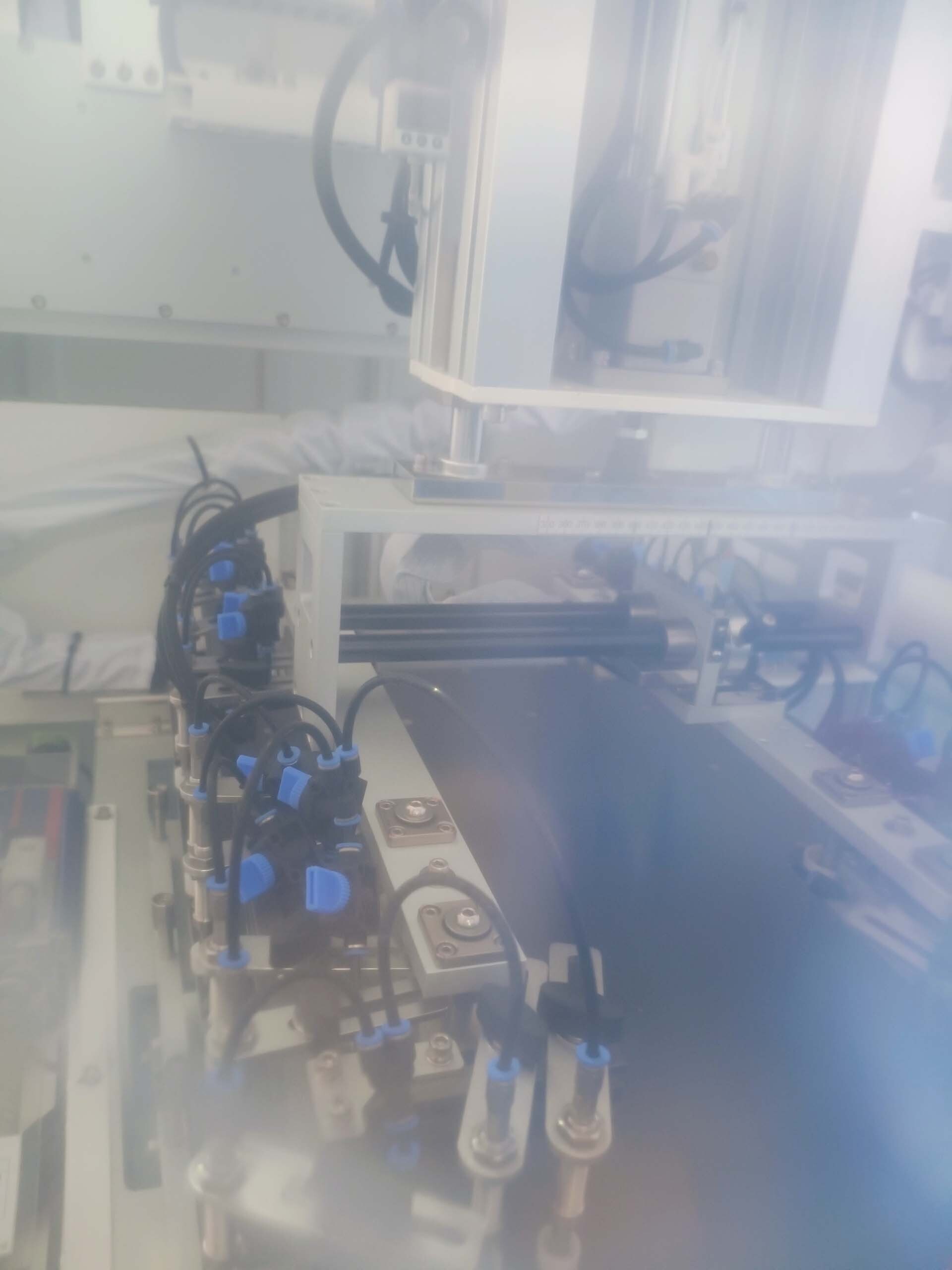
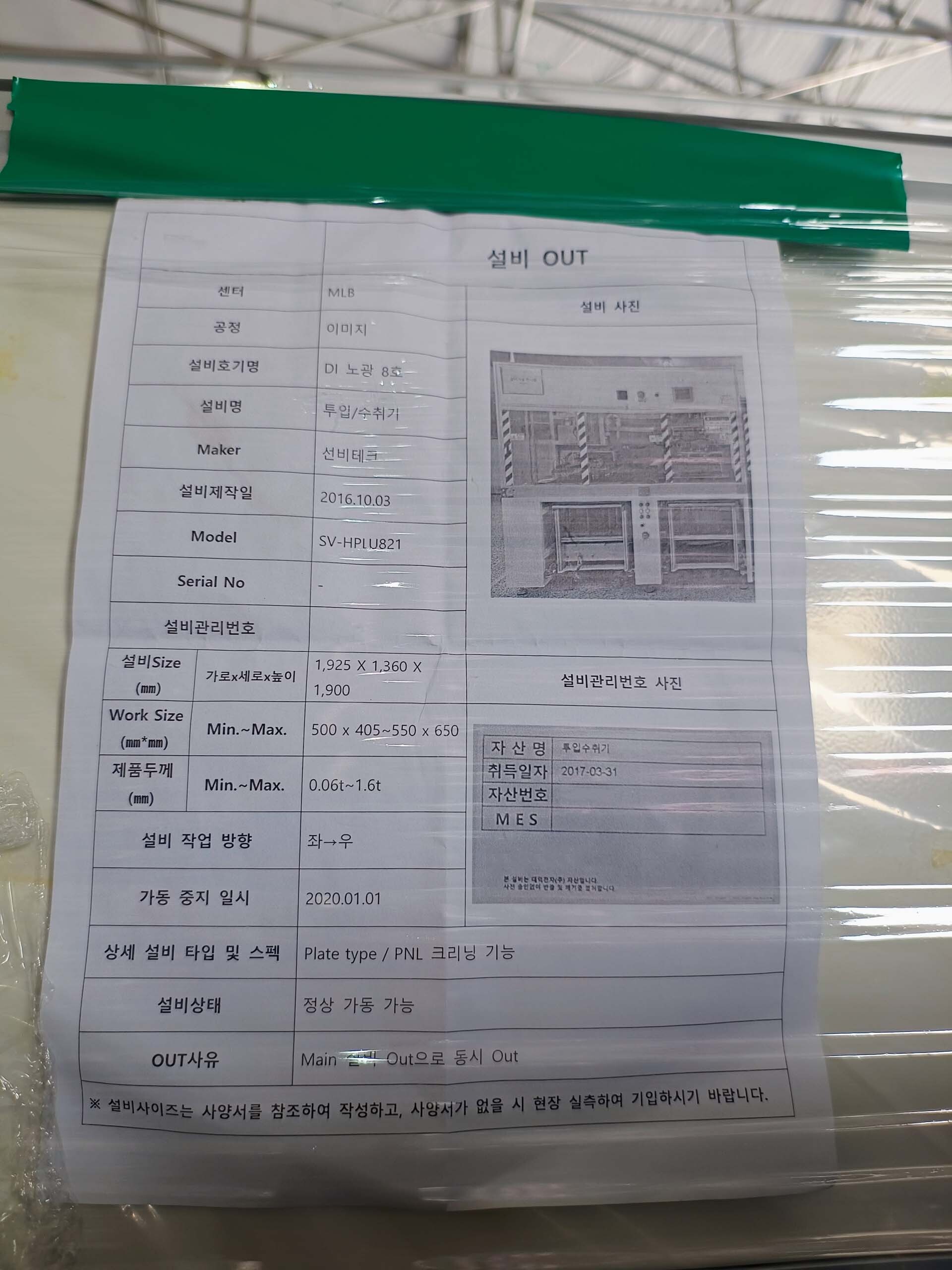
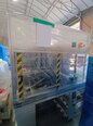
SEONBI SV-HPLU821 is a cutting-edge wafer testing and metrology equipment designed to provide comprehensive and precise analysis of semiconductor wafers. This advanced system integrates innovative technologies to ensure accurate measurements, fast data acquisition, and high throughput for semiconductor manufacturing processes. At the core of SV-HPLU821 unit is its wafer handling and positioning unit, which is equipped with precision robotics and advanced sensors to securely hold and maneuver wafers during testing and metrology processes. This unit ensures precise alignment and positioning of wafers, minimizing errors and enhancing the machine's overall reliability. The tool features a high-performance optics module that includes state-of-the-art imaging and spectroscopy components for capturing detailed images and spectral data from the semiconductor wafers. The optics module provides high resolution and sensitivity to detect subtle defects, contaminants, and variations in the wafer surface, enabling thorough characterization and analysis. One of the key highlights of SEONBI SV-HPLU821 asset is its advanced testing capabilities, which include electrical measurements, optical inspections, and material characterization. The model is equipped with multiple testing channels and probes that can simultaneously measure various properties of the wafer, such as electrical conductivity, optical transparency, and material composition. Moreover, SV-HPLU821 equipment is integrated with sophisticated software for data acquisition, analysis, and visualization. The software allows users to customize testing protocols, set measurement parameters, and generate detailed reports for easy interpretation of results. Additionally, the software is equipped with advanced algorithms for defect detection, pattern recognition, and statistical analysis to streamline the decision-making process in semiconductor manufacturing. SEONBI SV-HPLU821 system is designed to meet the demanding requirements of semiconductor fabrication facilities, offering high reliability, repeatability, and accuracy in wafer testing and metrology. The unit's modular design allows for easy customization and scalability to accommodate different wafer sizes, materials, and testing needs. In terms of performance, SV-HPLU821 machine excels in speed and efficiency, with fast data acquisition and analysis capabilities that significantly reduce testing time and improve productivity in semiconductor production lines. The tool's high throughput and automation features enable seamless integration into manufacturing processes, enhancing overall efficiency and yield in wafer production. Overall, SEONBI SV-HPLU821 wafer testing and metrology asset represents a state-of-the-art solution for semiconductor manufacturers seeking precise and reliable analysis of wafer properties. With its advanced technologies, comprehensive testing capabilities, and user-friendly interface, the model is poised to set new standards in semiconductor metrology and quality control.
There are no reviews yet