Used SSI Optical measurement system #293755214 for sale
URL successfully copied!
Tap to zoom
ID: 293755214
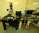
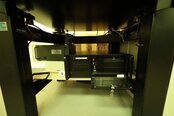
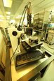
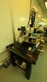
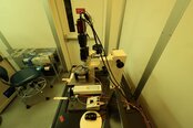
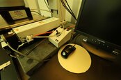
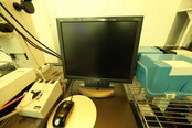
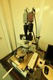
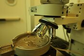
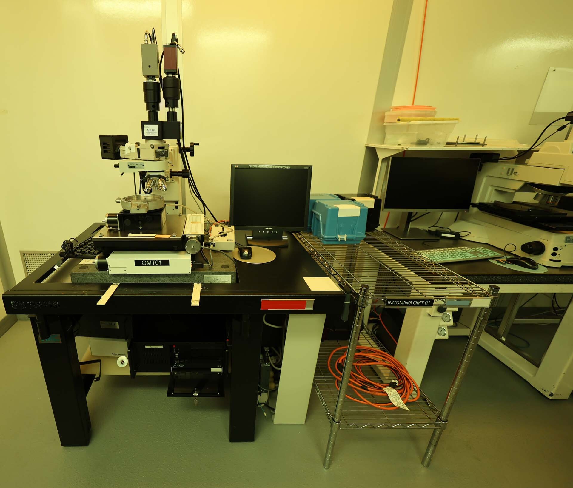
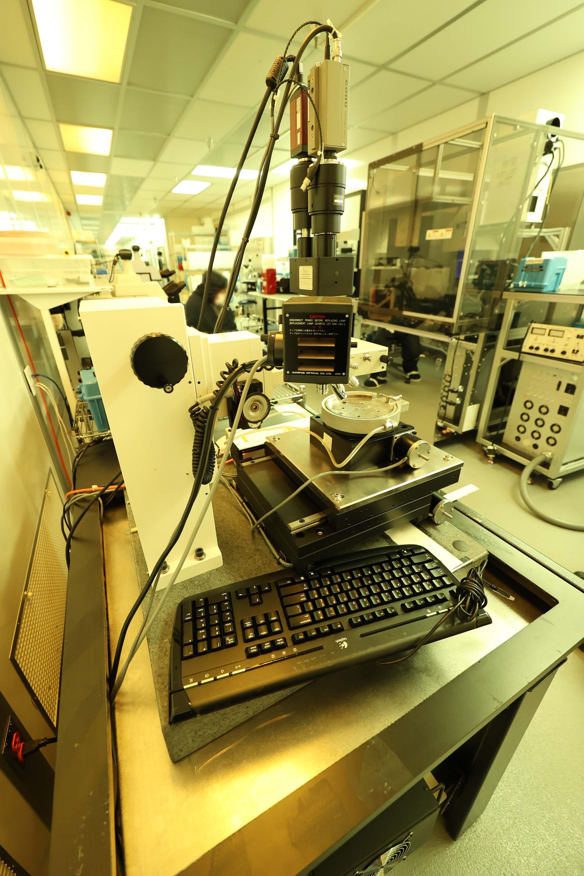
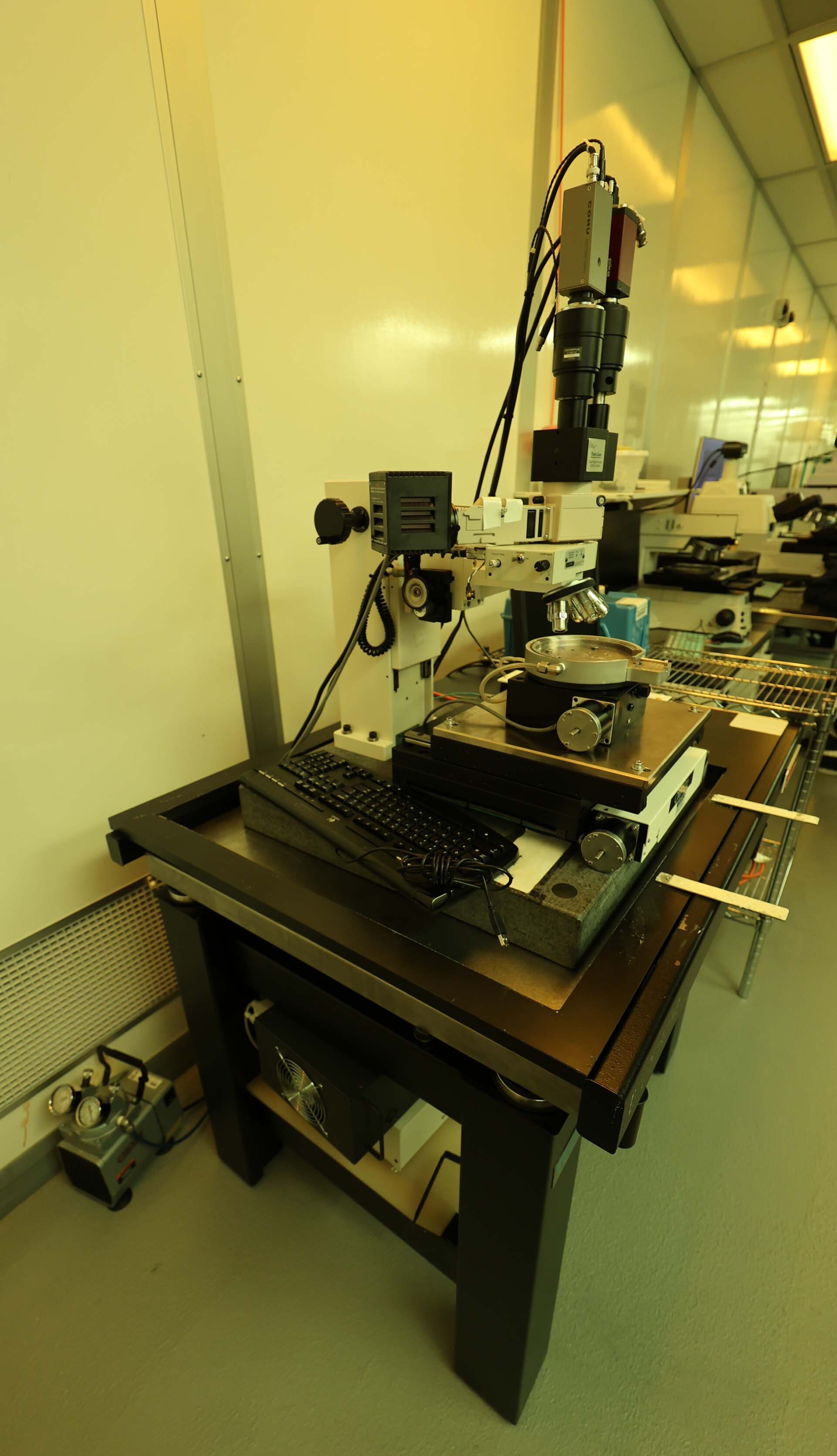
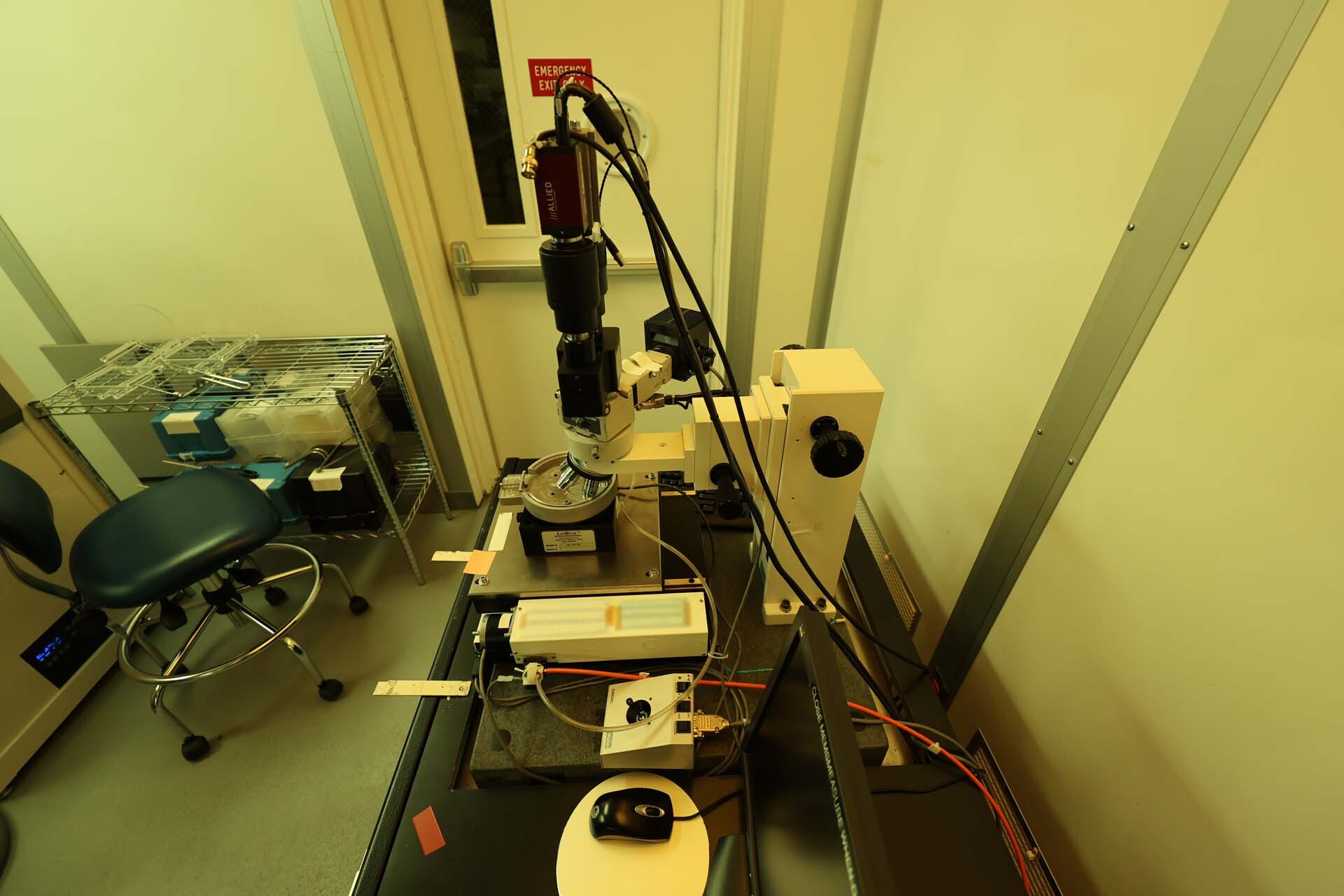
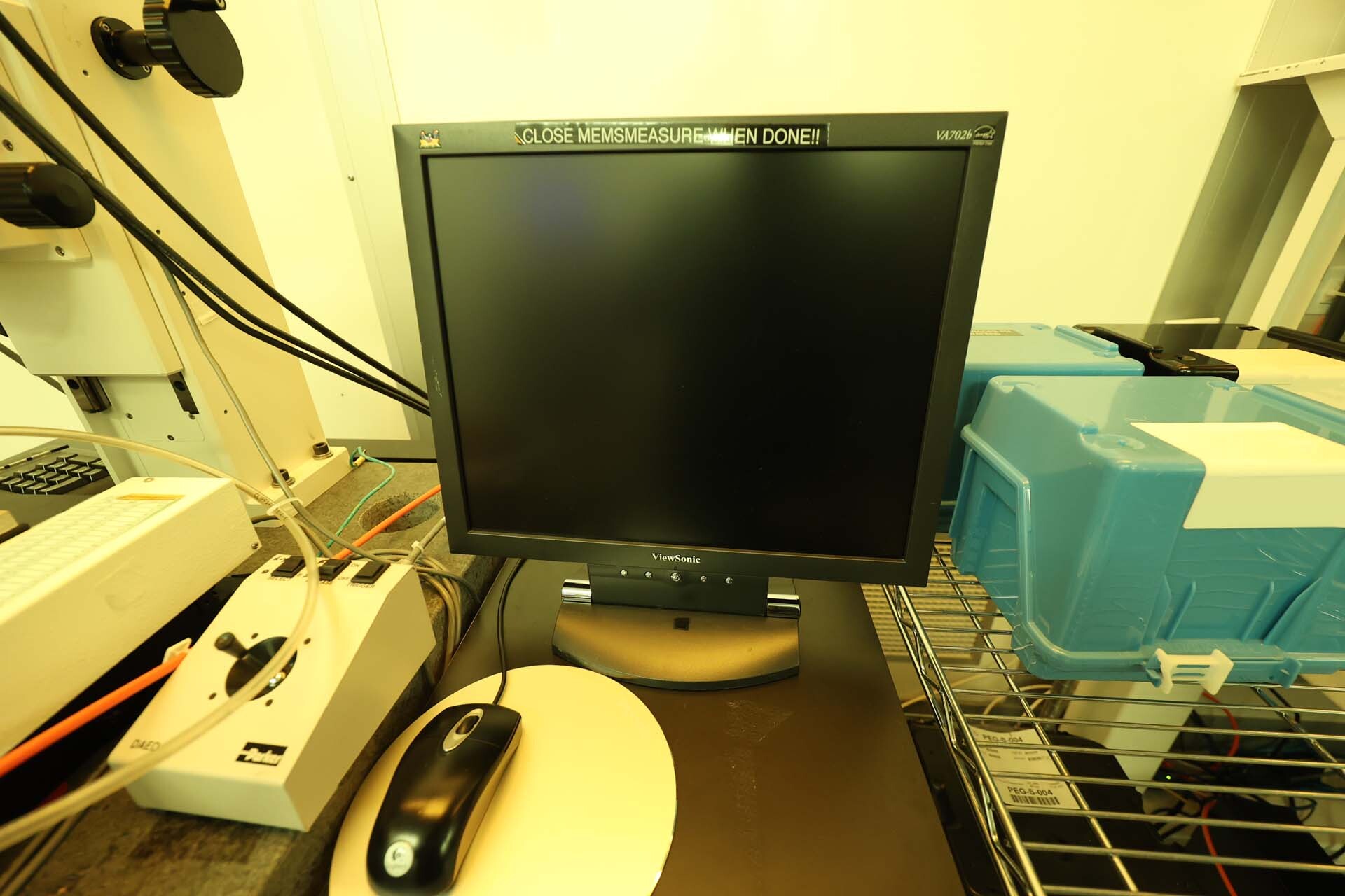
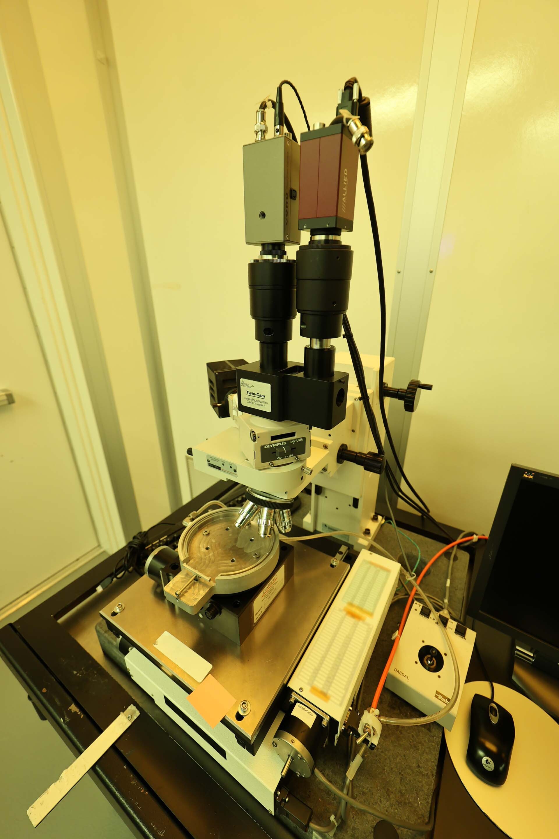
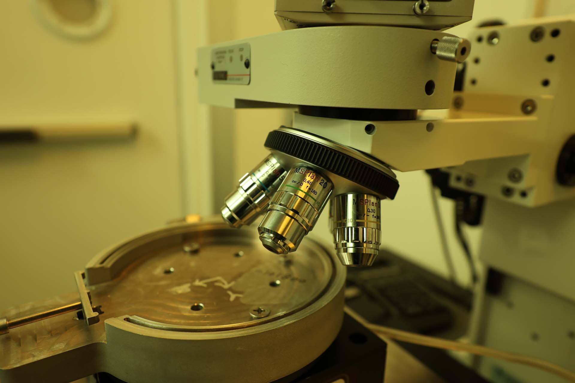
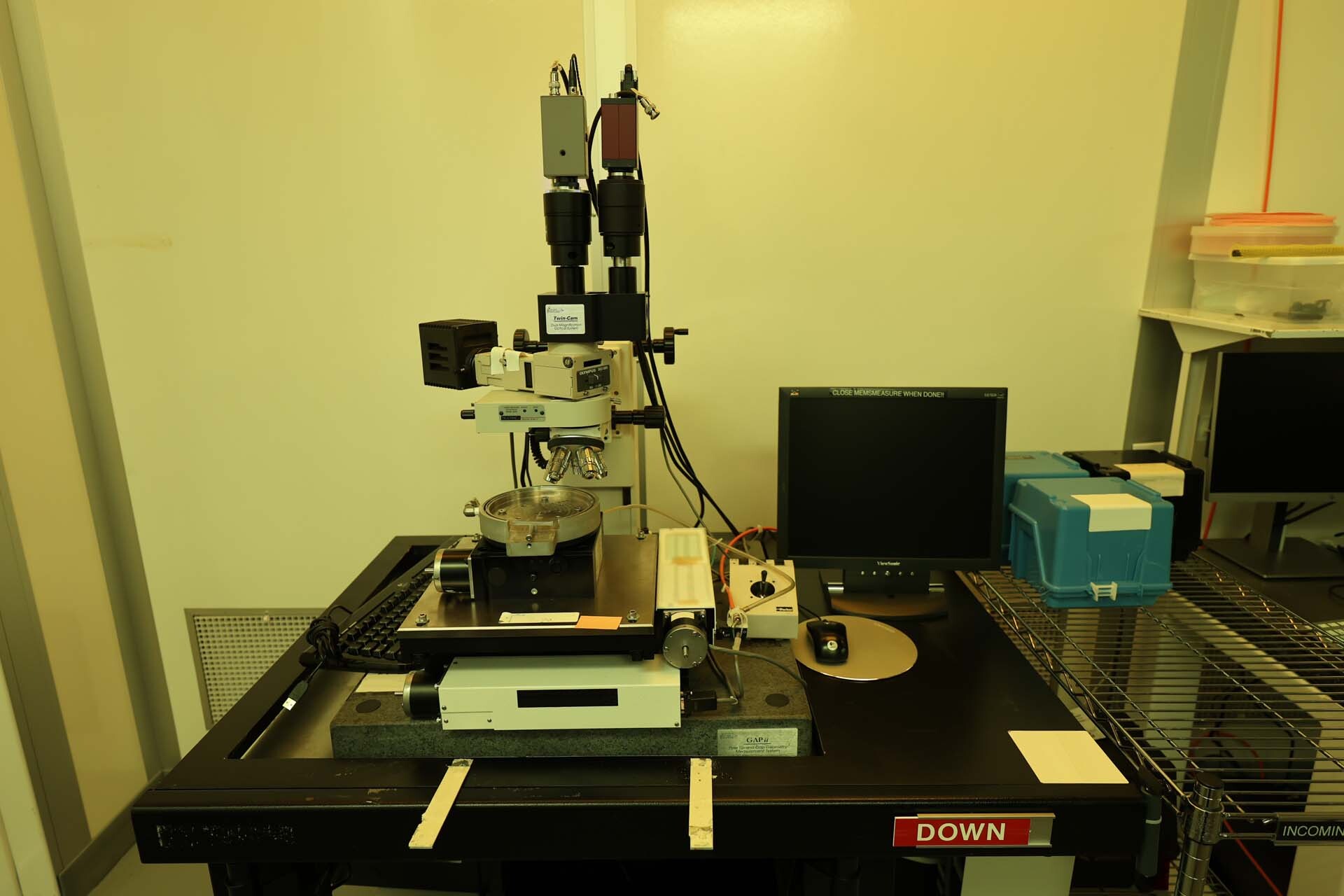
SSI Optical measurement equipment is a state-of-the-art wafer testing and metrology system designed to provide comprehensive and accurate measurement data for semiconductor wafers. This advanced unit utilizes optical technologies to analyze various parameters of the wafers, including dimensions, thickness, flatness, roughness, and defect inspection. Optical measurement machine is an essential tool for semiconductor manufacturers to ensure the quality and performance of their wafers before they are processed further in the production line. One of the key features of SSI Optical measurement tool is its high-resolution imaging capabilities. The asset uses advanced optical sensors and cameras to capture detailed images of the wafer surface with sub-micron resolution. These images are then analyzed using sophisticated image processing algorithms to extract precise dimensional information such as feature sizes, shapes, and positions. This allows for accurate measurement of critical dimensions on the wafer, which is essential for maintaining the quality and consistency of semiconductor devices. In addition to dimensional measurements, Optical measurement model also provides detailed information on the thickness and flatness of the wafer. By using optical interference techniques, the equipment is able to measure the thickness of the wafer with nanometer-level precision. This data is crucial for ensuring uniformity in the wafer thickness across its entire surface, which is essential for consistent device performance. The system also uses advanced phase-shifting algorithms to measure the flatness of the wafer, providing valuable insights into surface quality and potential sources of defects. Moreover, SSI Optical measurement unit is equipped with advanced software algorithms for defect inspection and classification. The machine can scan the entire surface of the wafer and detect various types of defects, such as particles, scratches, and pattern deviations. The tool uses machine learning techniques to classify these defects based on their size, shape, and location, allowing manufacturers to identify and eliminate sources of yield loss in their production process. Additionally, the asset can generate comprehensive defect maps and reports for further analysis and process optimization. Furthermore, Optical measurement model is designed for high-throughput operation to meet the demands of modern semiconductor manufacturing environments. The equipment features automated wafer handling and alignment capabilities, allowing for rapid and efficient measurement of multiple wafers in a single run. The system is also fully integrated with industry-standard wafer mapping and automation software, enabling seamless data transfer and process control across the production line. This integration ensures consistency and traceability in the measurement data, enabling manufacturers to make informed decisions and improvements in their manufacturing processes. In conclusion, SSI Optical measurement unit is a cutting-edge solution for wafer testing and metrology in the semiconductor industry. With its advanced optical technologies, high-resolution imaging capabilities, precise dimensional measurements, defect inspection algorithms, and high-throughput operation, the machine provides semiconductor manufacturers with the tools they need to ensure the quality, reliability, and performance of their semiconductor wafers. By leveraging the capabilities of Optical measurement tool, manufacturers can optimize their production processes, reduce defects, and improve the yield and reliability of their semiconductor devices.
There are no reviews yet