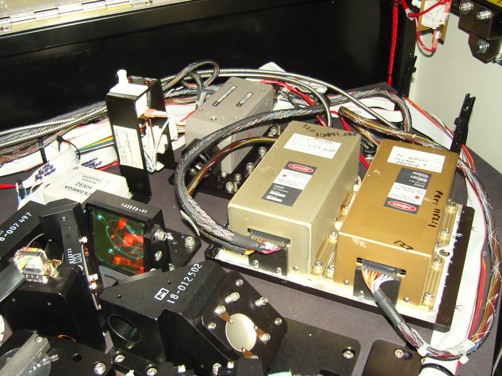
Used THERMA-WAVE TP 500 #146074 for sale
It looks like this item has already been sold. Check similar products below or contact us and our experienced team will find it for you.
Tap to zoom


Sold
ID: 146074
Wafer Size: 1997
Dose monitoring metrology system, 6" to 8"
Specifications:
Upgraded to XP in 2006
Probe and pump lasers replaced: fiber laser
Usage: processed implant wafers
(2) Open cassettes
Handler: EQUIPE robot and controller
IG byte tape drive
SECS II: GEM SECS Ver 2.06
COGNEX 5000 pattern recognition system
Back plane: Eisa Bus
Laser type:
Diode 10mW class IIIB probe laser
Diode 70mW class IIIB pump laser
Ion dose measurements: high dose
Dose range:
Boron: N/A
Phosphorous: 3E14 to 2E16
Arsenic: 1E14 to 2E16
BF2: 2E14 to 2E16
Energy range: 0.5 keV to 200 keV (all species)
TW repeatability: 0.5% 1-sigma TW
Power requirements: 110-220V, 20A
Utilities requirements: CDA 1/4", (2) vacuum 1/4" (stage, robot)
Includes service / operational manual and reference block
1997 vintage.
THERMA-WAVE TP 500 is a wafer testing and metrology system designed to characterize next-generation substrate materials. It uses advanced infrared technology to elucidate the physical and electrical characteristics of semiconductor, thin film, and other materials. Its specialized custom probes can be easily foundered to the base of a wafer substrate to collect accurate thermal mapping data with minimal impact on the device's thermal budget. THERMA-WAVE TP500 utilizes the measurement of thermomechanical properties such as thermal capacity, dielectric behavior, and thermal junction resistance to accurately determine the vulnerable characteristics of test wafers in the rapid development of new materials and process methods. Its infrared camera matrix offers the capability to capture images at high speed, enabling analysis of up to 1000 points per second. The ability to record up to 80 different tests at the same time allows for extremely accurate data collection and metrology with minimal expenditure of time and resources. The high-resolution, thermal gradient of temperature difference helps to avoid costly wafer loss due to material defects. Additionally, TP-500's pixel addressable digital input options ensure result consistency and accuracy with minimal effort. Advanced data analysis, synchronization, and reporting give the user detailed information regarding the performance of their devices and processes. Furthermore, TP500 offers a wide range of benefits to the user. Its compatibility with various PC-based platforms allows easy integration into existing systems. Its fast, online data recording and acquisition time minimizes the time and costs associated with data logging. Its analysis mode quickly identifies any weak points or errors in the results and gives the user the ability to quickly modify their processes or material to immediately mitigate them. Overall, TP 500 is a powerful system for testing and metrology of wafer materials. It can be easily integrated into existing systems and is capable of capturing the most intricate details in a short period of time. Through its precision measurement capabilities and detailed data analysis, it is a powerful tool for material characterization in the rapid development of next-generation substrate materials.
There are no reviews yet