Used VEECO / BRUKER / SLOAN DEKTAK XT #293812083 for sale
URL successfully copied!
Tap to zoom
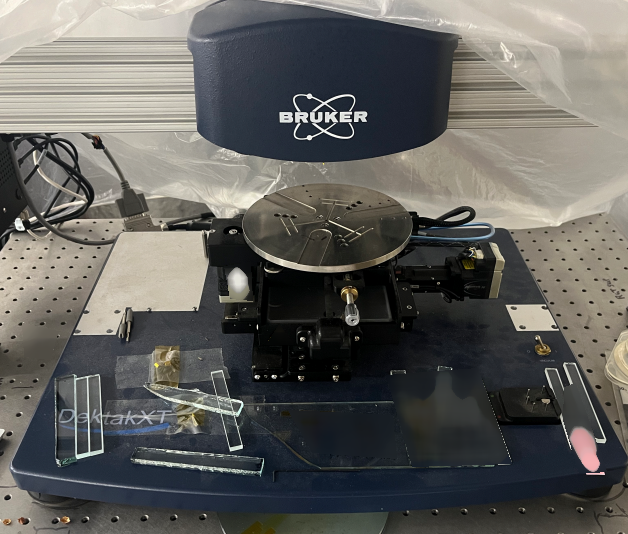

VEECO / BRUKER / SLOAN DEKTAK XT is a next-generation wafer testing and metrology equipment that provides high-precision 3D nano-scale surface shape measurements. The system is designed to increase throughput and reduce the cost of production for high-volume manufacturers of microelectronic components. The unit uses a custom-built, contact-based stylus profilometer for accurate, repeatable, and reliable measurements. The stylus profile is capable of measuring more than 500 different points every second. The measurements are taken directly from the wafer surface, allowing for high accuracy and repeatability. The machine also offers its automated wafer aligner (AWA) for high-precision, fast, and accurate placement of the wafer in the correct position for scan field measurements. The AWA is designed to make real-time corrections to ensure that the stylus is always contacting the same surface point on the various individual die on a wafer during successive scans. In addition to its hardware components, the tool includes a variety of software applications to facilitate wafer testing and metrology. For example, its multi-level feature measurement application enables highly accurate and repeatable measurements. The asset's automated feature recognition (AFR) model works in conjunction with this application, to quickly and accurately detect critical features of wafers. The equipment also includes the high-speed edge detection and review (EDR) application. This features allows operators to rapidly review edge conditions and high spatial-resolution particles and contaminants on wafers within seconds. The system also has a comprehensive feature identification/classification (FIC) unit to quickly identify and classify a variety of feature types. VEECO DEKTAK XT machine helps to significantly reduce production time and costs for a variety of applications. It leverages advanced technologies and tools to quickly and accurately measure nanoscale features on wafers. Its automated aligner and feature recognition technologies pave the way for faster wafer testing and metrology. As such, it is an excellent solution for high-volume manufacturers of microelectronic components who wish to quickly and accurately measure nano-scale features on wafers.
There are no reviews yet