Used WYKO / VEECO HD 3300 #293775829 for sale
URL successfully copied!
Tap to zoom
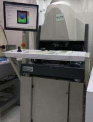

WYKO / VEECO HD 3300 is a state-of-the-art wafer testing and metrology equipment designed for precise and accurate measurement of surface quality, roughness, and topography of semiconductor wafers and other substrates. This sophisticated system incorporates advanced imaging and measurement technologies to provide semiconductor manufacturers with critical data for process optimization and quality control in wafer fabrication. At the core of WYKO HD 3300 unit is a high-resolution optical profiler that uses non-contact interferometry to capture detailed surface profiles with nanometer-scale resolution. This profiler utilizes laser technology to scan the surface of the wafer and generate three-dimensional maps of surface features. The machine is equipped with advanced software algorithms that can analyze the data and provide valuable insights into surface roughness, waviness, step heights, and other topographical parameters. VEECO HD 3300 tool is capable of measuring a wide range of substrate materials, including silicon, gallium arsenide, sapphire, and other compound semiconductors commonly used in the industry. The asset offers flexibility in terms of sample size and shape, allowing users to analyze wafers of various diameters and thicknesses. This versatility makes the model suitable for a diverse range of applications in semiconductor manufacturing, research, and development. One of the key features of HD 3300 equipment is its advanced automation capabilities, which streamline the measurement process and minimize operator intervention. The system can be programmed to perform sequential measurements on multiple wafers with high repeatability and accuracy, reducing the risk of human error and ensuring consistent results across different samples. This automation feature is particularly advantageous for high-throughput manufacturing environments where efficiency and productivity are paramount. WYKO / VEECO HD 3300 unit also offers a range of analysis tools and options for data visualization, allowing users to extract valuable insights from the measurement data. Users can generate detailed surface roughness maps, cross-sectional profiles, and statistical reports to evaluate the quality of the wafer surface and identify any defects or irregularities that may impact device performance. The machine can also perform advanced data processing tasks such as filtering, stitching, and merging datasets to enhance the accuracy and reliability of the measurements. In conclusion, WYKO HD 3300 wafer testing and metrology tool is a cutting-edge solution for semiconductor manufacturers seeking precise and reliable surface characterization of wafers. With its advanced imaging capabilities, automation features, and comprehensive analysis tools, the asset provides users with the critical information they need to optimize process parameters, improve yield, and ensure the quality of semiconductor devices. VEECO HD 3300 model represents a significant advancement in wafer metrology technology and is poised to play a vital role in the ongoing evolution of the semiconductor industry.
There are no reviews yet