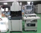
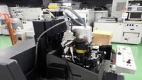
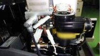
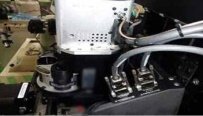
Used WYKO / VEECO NT 3300 #9151517 for sale
URL successfully copied!
Tap to zoom
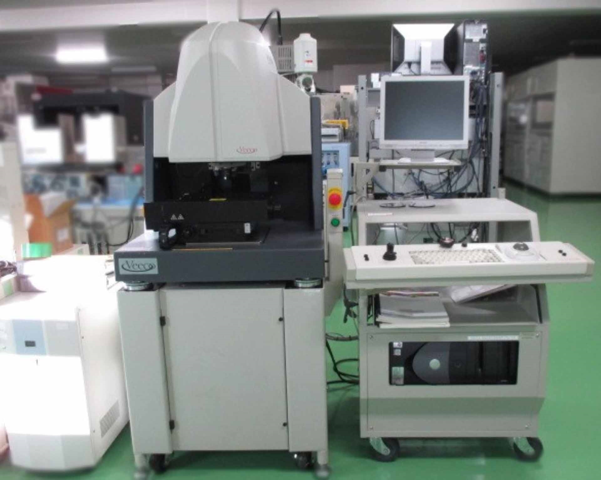




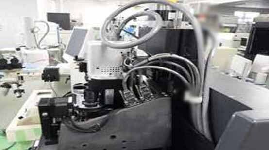


WYKO / VEECO NT 3300 is a signal-processing-based wafer testing and metrology equipment. It is used to analyse the electrical properties of semiconductor devices such as diodes, transistors, capacitors, and resistors. WYKO NT 3300 has a high-resolution imaging system that provides dimensional characteristics of the device inspects and results of wafer probing and tests. The images can be captured using a range of configurations, such as light, dark, and grey-scale. VEECO NT 3300 offers a wide range of wafer probing and testing capabilities. This includes high-efficiency, ultra-fast scan of a wafer or a group of die across a wide range of parameters and operating conditions. NT 3300 can also perform automated wafer plotting, defect analysis, device profiling, parameter extraction, parametric measurement and IV statistical analysis. Furthermore, the unit is equipped with a high-speed image analysis tool which is used to analyse data from the wafer probing and schematic analysis. This tool provides comprehensive device characterization that includes the measurement of the device's on-resistance, thermal parameters, signal propagation-speed, and capacitance. This information is then used to design the optimised production parameters for the device under review. WYKO / VEECO NT 3300 is designed with an integrated architecture to ensure efficient wafer probing and testing. It uses an integrated analog signal-processing platform comprising of an acquisition module, signal processing module, and a control module. The acquisition module is responsible for capturing the signals obtained from the device being tested, while the signal processing module applies mathematical filters to these signals. These filters equate to precision measurements that produce comparative data of the device's performance and actual design specifications. WYKO NT 3300 control module then manages all the operations of the testing machine. It provides an intuitive interface that allows the user to select the device and test parameters, analyse the results, and manage application configurations. Thus, VEECO NT 3300 ensures a smooth and time-effective wafer probing and testing process. In conclusion, NT 3300 is a wafer probing and metrology tool designed to analyse the electrical parameters of semiconductor devices. With its high-resolution imaging asset, automated wafer plotting and defect analysis capabilities, in-situ image analysis tool and an integrated architecture, WYKO / VEECO NT 3300 is a powerful tool for device characterisation, high-efficiency probing and testing and the design of optimised production parameters.
There are no reviews yet
