Used TEL / TOKYO ELECTRON Clean Track Mark 7 #293620432 for sale
URL successfully copied!
Tap to zoom


ID: 293620432
Wafer Size: 8"
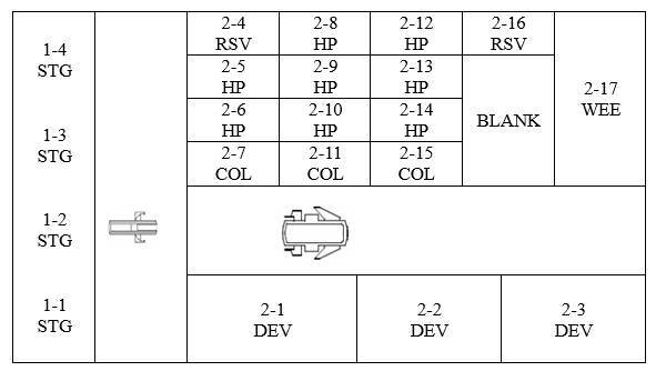
(1) Coater / (3) Developer system, 8"
Process: i-Line develop unit
Power transformer
S2-93
Developer:
Stream nozzle
Top rinse nozzle
Back rinse nozzle
Temperature control
Motor flange temperature control
Direct gravity drain
Auto damper
External chemical cabinet:
TEL OEM SMC Thermo controller (5-Channels)
Wafer direction:
Left to right
Right to left
1994-1996 vintage.
TEL / TOKYO ELECTRON Clean Track Mark 7 is a photoresist processing equipment designed specifically for the automated development of semiconductor devices. The system utilizes a deposition process tocoat a wafer surface with photoresist coating material, which then is exposed to UV light to form a desired pattern. The pattern is then developed and transferred onto the wafer through etching. TEL Clean Track Mark 7 unit consists of a dual-level spin-track for etching and a vacuum machine, both of which are connected by integrated control electronics. The spin-track has two chambers: the upper chamber is used for the deposition of photoresist, while the lower chamber is used for the exposure of the material to UV light. The vacuum tool provides vacuum pressure for etching and for removing the photoresist from the work surface. TOKYO ELECTRON Clean Track Mark 7 comes with a range of advanced features, including an automated transfer asset, a dummy substrate handling mechanism, extended temperature range control, air supply pressure control, cooling control, wafer aligner, and an integrated defect monitoring model. The integrated control electronics are highly configurable and provide a wide range of functionality such as wafer parameter setting, recipe management, and generated yield monitoring. The equipment also includes a range of advanced safety features to protect personnel, such as the interlock switch and temperature sensor. Finally, Clean Track Mark 7 supports a wide variety of photoresist materials and is designed for increased process efficiency. The system also features a high degree of automation and control which can improve the speed, accuracy and repeatability of the depositing, developing, and etching stages of photoresist processing.
There are no reviews yet

