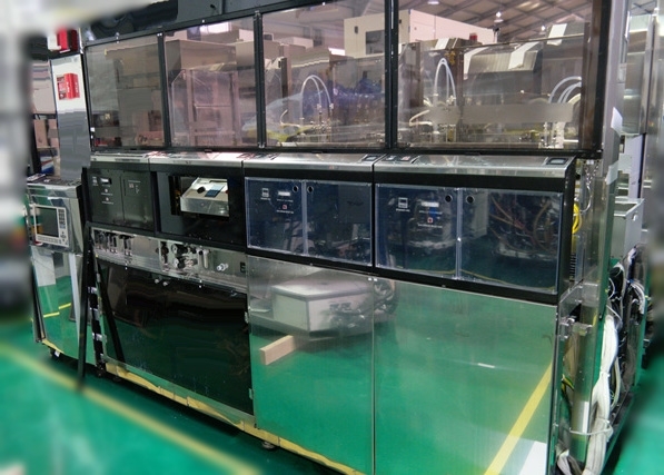
Used TEL / TOKYO ELECTRON Clean Track Mark 7 #9192134 for sale
It looks like this item has already been sold. Check similar products below or contact us and our experienced team will find it for you.
Tap to zoom


Sold
TEL / TOKYO ELECTRON Clean Track Mark 7 is one of the leading photoresist systems available worldwide. It provides high accuracy, precision and uniformity for recessed, sprayed and sputtered patterns in the production of integrated circuits. This platform is the result of years of research and development, offering unparalleled precision and feature resolution. TEL Clean Track Mark 7 photoresist equipment features high-precision lithography algorithms and a highly stable optical system. This ensures both consistent lithographic performance and precise measurement of features. Additionally, the lithography unit uses an advanced optical architecture known as hybrid recessed optics to reduce aberrations and increases operation speed. This machine also features an anti-reflective coating to reduce the scattering of light at the wafer surface, yielding even greater image fidelity. TOKYO ELECTRON Clean Track Mark 7 is ideal for photomasking, where high resolution integrated circuit patterns can be reliably generated. This tool also features a unique angulated recessed optical asset, allowing for the creation of unique angled photomasks. Additionally, the model uses advanced exposure systems that minimizes edge-roughness and ensures critical dimensional accuracy. Finally, the equipment incorporates a high-powered wafer handling system. This feature ensures that wafer handling does not perturb the wafer at any time, thus maintaining safety. It also ensures that wafers maintain proper alignment and are perfectly cleared by the exposure unit to get the desired pattern on the chip surface. Further, its advanced wafer transport machine allows for quick and easy transfer of wafers into and out of Clean Track Mark 7 tool. In summation, TEL / TOKYO ELECTRON Clean Track Mark 7 is an advanced photoresist asset which incorporates a high accuracy, precision and uniformity for recessed, sprayed and sputtered patterns. This model is a robust and reliable platform for creating integrated circuit patterns. Additionally, its angulated recessed optics and advanced exposure systems make it ideal for photomasking processes. Finally, its advanced wafer handling equipment ensures the safety of wafers and their easy transfer into and out of the system.
There are no reviews yet