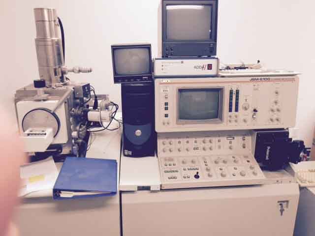
Used JEOL JSM 6100 #9157307 for sale
URL successfully copied!
Tap to zoom


JEOL JSM 6100 is a scanning electron microscope (SEM) that utilizes secondary electrons (SE) to produce high resolution images of samples in an electron microscope. JSM 6100 is a variable pressure scanning electron microscope that allows the operator to vary the pressure of the chamber from a high pressure of .3 pascals (roughly 2 millitorr) to a low pressure of 10-6 pascals (roughly 30 nanotorr). This range of pressure allows imaging of non-conducting samples by reducing the charging effect. The specimen stage can rotate 360° with a tilt range of -80° to +90° making it ideal for oblique imaging. The specimen stage can also assist the operator with specimen height adjustment. The sample can placed in a holder and raised to the objective lens which has a short working distance of only 8mm, making it ideal for small samples that require high magnification. This high magnification is made possible due to the lens magnification range of 5x to 45,000x. JEOL JSM 6100 also has two 30 kV SE detectors designed to be used at the same time, each detector has a magnification range of 30x to 20000x. JSM 6100 is equipped with an Everhart-Thornley Type SE detector that is used for imaging conductive and non-conductive samples. This detector uses a Faraday cup to detect the electron backscatter and a solid state detector (TED) to detect the secondary electrons. The Everhart-Thornley SE detector has a wide dynamic range and resolution to bring out fine details on the sample surface. The Everhart-Thornley SE detector can be combined with the second detector, a diverging long-emission electron source (LEED), to extend the detection range to the atomic scale. The LEED allows for imaging of non-conductive surfaces and accurate determination of crystal structure. The LEED source has two apertures with manual control and the ability to vary the emission current from 0-100 nA. JEOL JSM 6100 is a powerful scanning electron microscope that is ideal for imaging samples with nanometer-scale resolution. It is capable of imaging non-conductive samples with excellent resolution and accuracy. JSM 6100 is an ideal tool for imaging conductive and non-conductive surface details, as well as atomic structure determining.
There are no reviews yet