Used ADE / KLA / TENCOR CR81e #293771795 for sale
URL successfully copied!
Tap to zoom
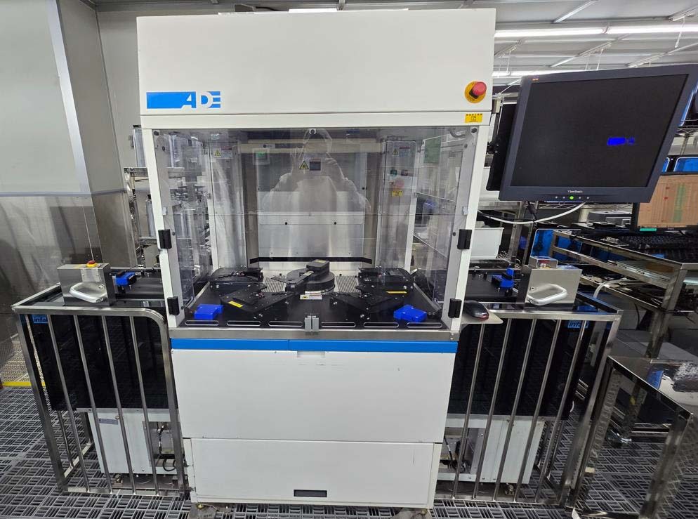

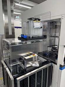
ID: 293771795
Vintage: 2003
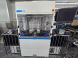
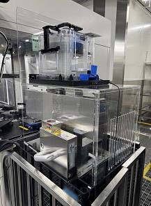
Wafer inspection system
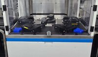
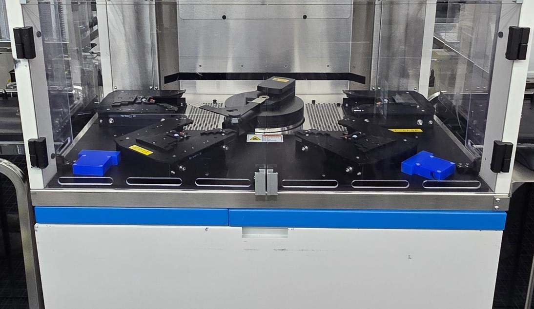
(4) Cassette stations
BROOKS AUTOMATION Load SMIF Robot arm
BROOKS AUTOMATION Unload SMIF Robot arm
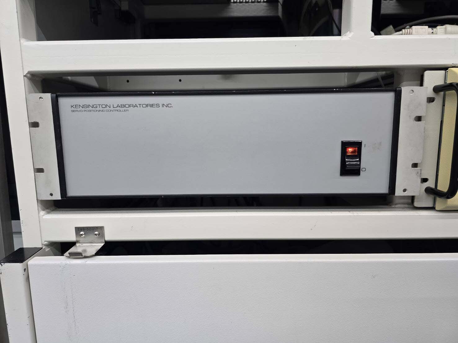
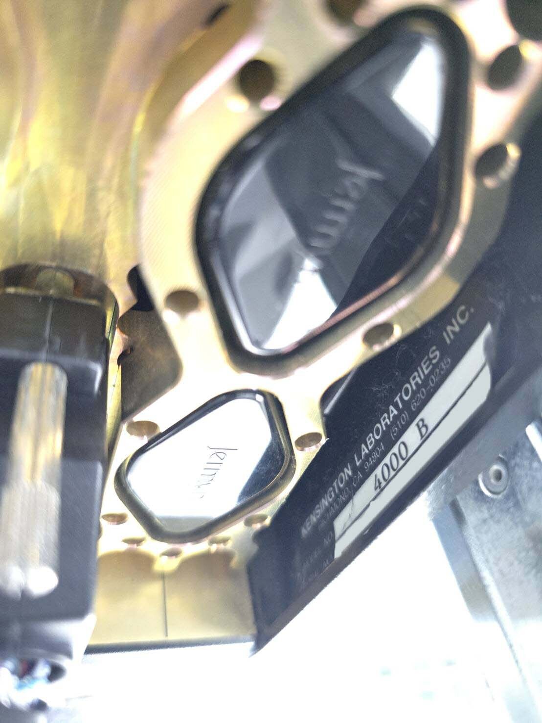
KENSINGTON Robot with controller
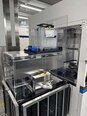
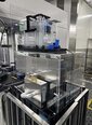
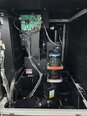
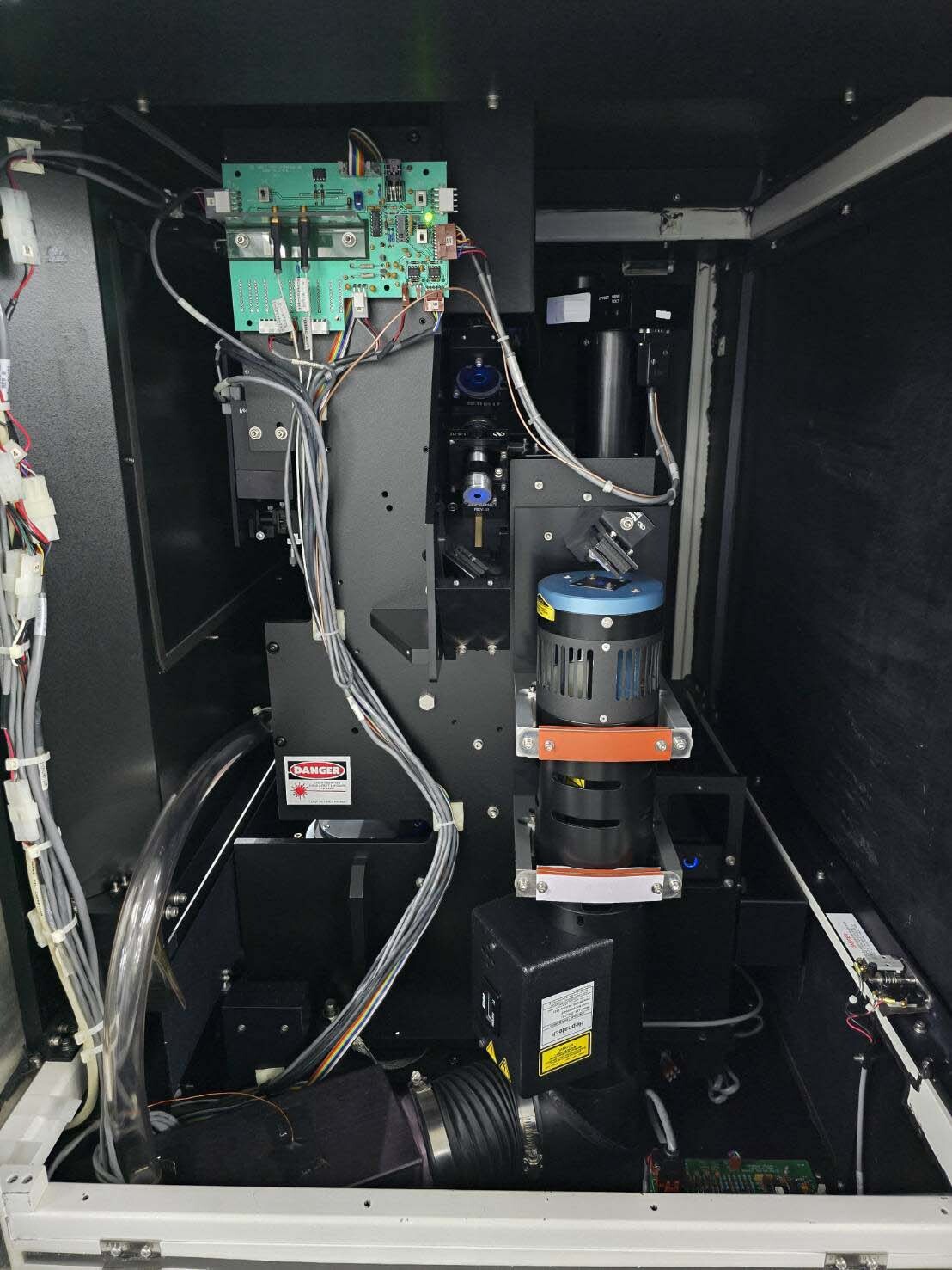
Inspection stage with optical module
Vacuum: 21 SCFH at 26" Hg
CDA: 81 PSI, 200 cu in/hr min
General exhaust: 4" Duct, 400 CFM
SSL Laser
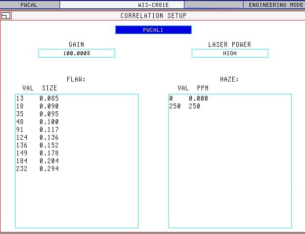
PSL Calibration
Particle sensitivity:
120 nm LSE
105 nm LSE
Spare parts for CR81e:
Part number / Description
12051137 / LAMBDA Power supply box
12051333 / Dark R268PMT group
12051134 / Bright channel light vacuum tube
12058488 / Air pressure
12051338 / Dark channel arc mirror
12051339 / Focal lengh lens 100MMFL 25.4 mm
12051340 / Robatic arm set
12051513 / Standard wafer supporter
122052995 / PMT Air traffic controller 0092493-001
120562228 / Collection group 398-20281-1
12058498 / KENSINGTON Arm tip
12058499 / KENSINGTON Edge alignment chuck
12114222 / 68060 array processing board 398-20406-1
12114223 / Bright channel analog board CH-0398-20883-1
12114226 / Bright channel analog board CH-1398-20884-1
12114227 / HAZE Tablet 398-20705-1
12114228 / Daek channel X-Axis plate (12BIT) 398-20733-1
12115229 / Bright channel X-Axis plate 398-20630-1
12114231 / Bright channel X-Axis plate CH-1398-20706-1
12114232 / Origin of the pulse plate 398-20841-1
12149175 / CCD Signal transmission board, Robatic arm, 03142
121499223 / CCD Brush, Robot arm, 031409-27
12178367 / Oppsosite signal receiving board, 031409-08
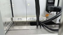
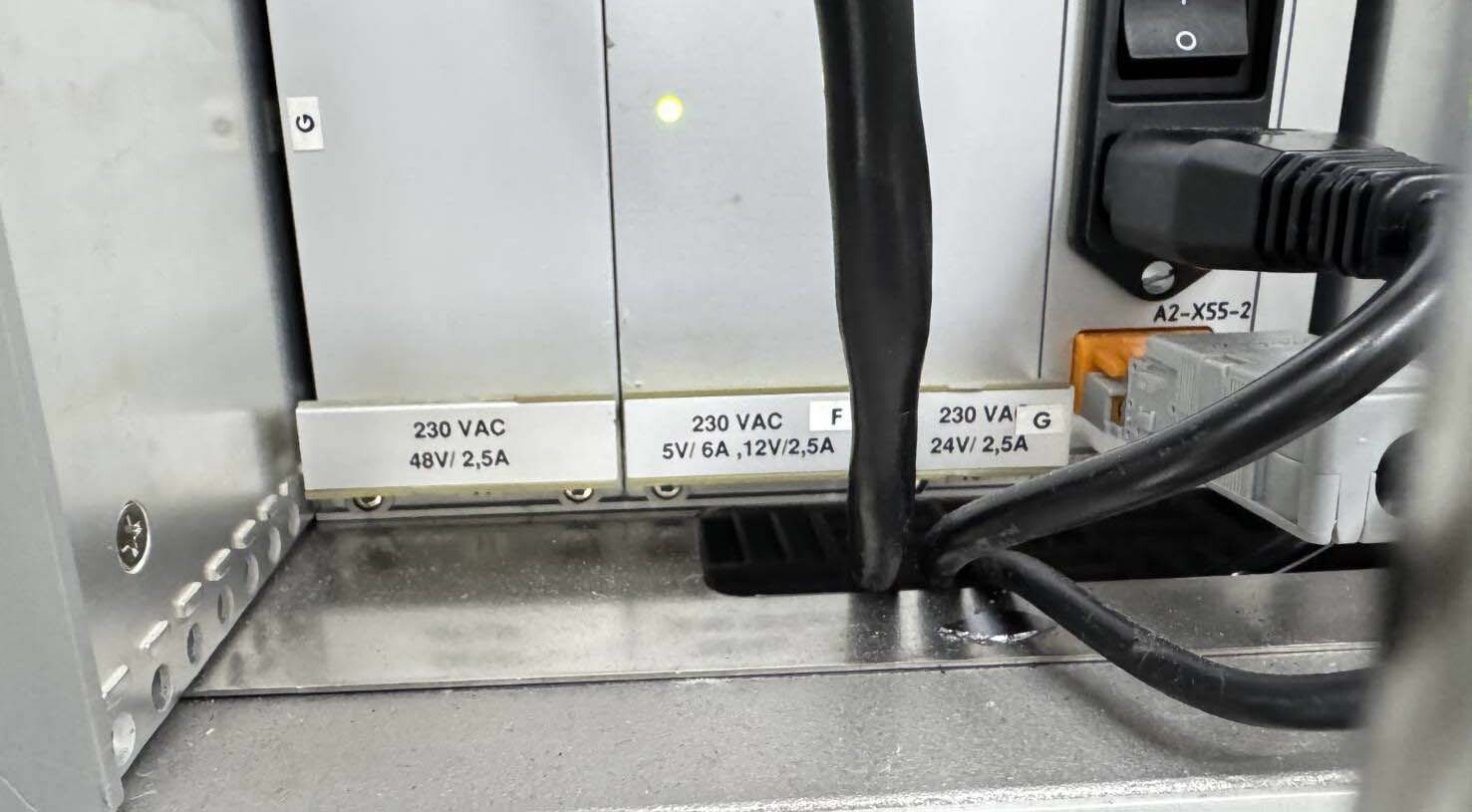
Power supply: 208 VAC, 30 Amps, 47-63 Hz, 3 Phase
2003 vintage.
ADE / KLA / TENCOR CR81e is an advanced wafer testing and metrology equipment designed for the semiconductor industry. It offers a comprehensive suite of capabilities for characterizing and analyzing semiconductor wafers to ensure the highest quality and performance of integrated circuits (ICs) produced on them. ADE CR81e is a highly sophisticated tool that integrates various measurement techniques to provide accurate and reliable data for process control and yield management in semiconductor manufacturing. One of the key features of KLA CR81e system is its ability to perform non-destructive testing on semiconductor wafers. This means that the unit can analyze the properties of the wafers without damaging them, allowing manufacturers to minimize material wastage and reduce costs. The machine uses a combination of optical, electrical, and physical measurement techniques to evaluate the key parameters of the wafers, such as thickness, topography, defect density, and electrical performance. TENCOR CR81e is equipped with advanced imaging capabilities, including brightfield, darkfield, and confocal microscopy, to visualize the structure and morphology of the wafers at high resolution. This allows users to inspect the surface quality, pattern uniformity, and defects present on the wafers with precision and accuracy. The tool also features automated image analysis algorithms that can quickly process large amounts of data to identify and classify defects for further analysis. In addition to imaging, CR81e utilizes advanced spectroscopy techniques, such as photoluminescence and Raman spectroscopy, to analyze the chemical composition and crystal structure of the wafers. These techniques provide valuable information about the material properties, dopant concentrations, and structural defects present in the wafers, which are critical for assessing the quality and reliability of the semiconductor devices fabricated on them. The asset can perform rapid and sensitive measurements to detect subtle variations in the composition and structure of the wafers, enabling manufacturers to optimize their processes for better performance and yield. Furthermore, ADE / KLA / TENCOR CR81e incorporates advanced metrology tools, such as atomic force microscopy (AFM) and ellipsometry, to measure the physical dimensions and optical properties of the wafers with nanometer-scale precision. These tools enable users to characterize the surface roughness, film thickness, and refractive index of the wafers, which are essential for controlling the layer deposition and etching processes in semiconductor fabrication. The model can generate detailed 2D and 3D maps of the wafer properties, providing valuable insights into the process variations and defects that may impact the device performance. Overall, ADE CR81e is a comprehensive wafer testing and metrology equipment that offers a wide range of capabilities for semiconductor manufacturers to evaluate the quality and reliability of their wafers. Its advanced imaging, spectroscopy, and metrology technologies enable precise characterization of the wafers' properties, helping to optimize manufacturing processes, improve device performance, and increase yield in semiconductor production. KLA CR81e is a powerful tool for quality control and process optimization in semiconductor manufacturing, making it an indispensable asset for ensuring the success of advanced semiconductor devices in the market.
There are no reviews yet