Used ADE / KLA / TENCOR MicRhoSense 6035 #9301379 for sale
URL successfully copied!
Tap to zoom


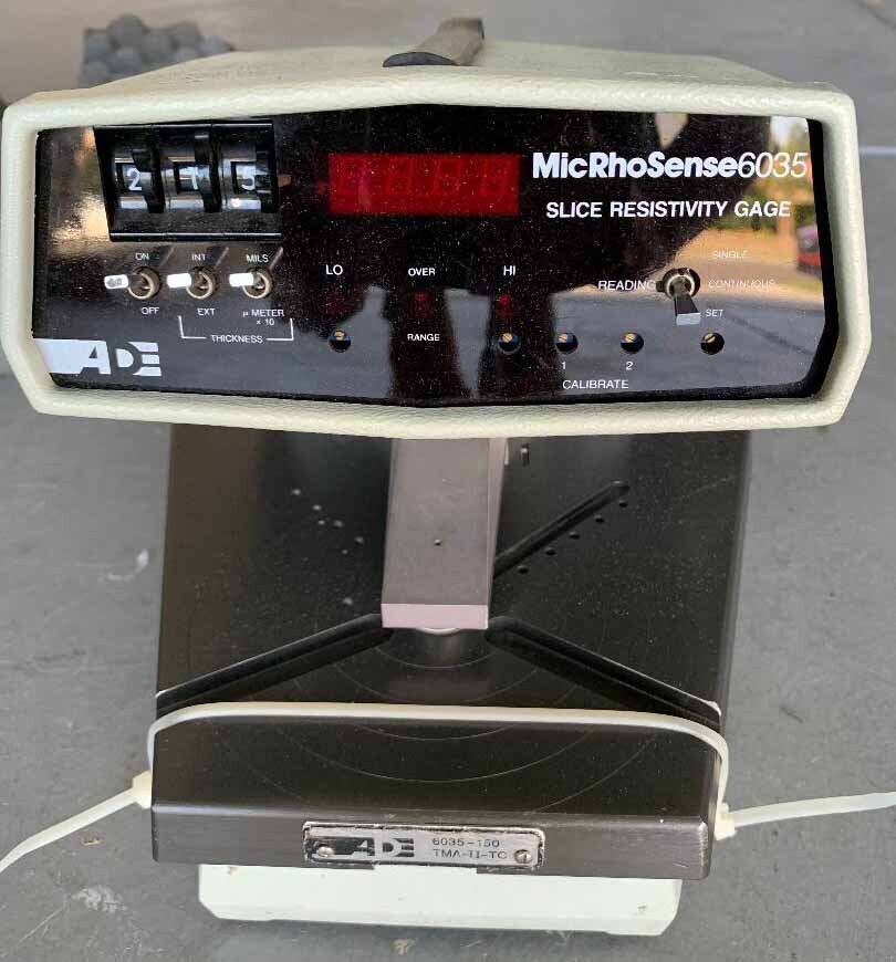
ADE / KLA / TENCOR MicRhoSense 6035 is an advanced wafer testing and metrology equipment. It is capable of producing highly accurate measurements that are key to wafer fabrication processes at semiconductor facilities. The system features a die-to-database architecture that allows for direct comparison of measurement results against reference photomasks and various semiconductor process nodes. This ensures that the wafer fabrication process is held to the highest standards of accuracy. ADE MicRhoSense 6035 incorporates several design elements to ensure accuracy, including an advanced pattern recognition feature and automated thresholding. This pattern recognition utilizes proprietary algorithms to determine the type of defect present, such as a short or open circuit, and then define the position of the defect relative to the reference photomask. This allows the unit to accurately measure the parameters of a given defect, such as height or area, and perform various types of defect analysis. KLA MicRhoSense 6035 also features a specialized alignment machine. This tool uses high precision optics and precise motion and rotary stages to ensure exact positioning of the wafer relative to the reference photomask. This enables precise measurements to be made with repeatable accuracy. Additionally, the asset features ultra-short wavelength laser metrology for high-precision measurements of critical dimensions. This is critical for evaluating wafer production yield and repeatability. MicRhoSense 6035 uses several inspection modes to ensure maximum accuracy of the results. These include contour mapping, defect detection and fault isolation, wafer mapping, and class-defect analysis. These modes are implemented in software algorithms that are capable of making far more precise measurements than with conventional inspection systems. Finally, TENCOR MicRhoSense 6035 features an intuitive user interface which allows for quick and easy setup and calibration of the model. Additionally, the equipment has access to an extensive library of setup parameters that can be customized as necessary for a given fabricator. This allows users to maximize accuracy and minimize setup time. All of these features combine to provide a comprehensive wafer testing and metrology system that is capable of handling the most demanding semiconductor fabrication processes.
There are no reviews yet

