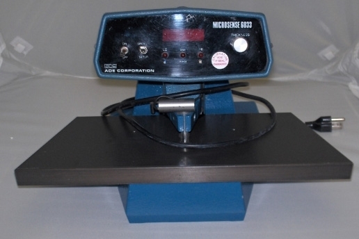
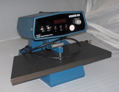
Used ADE / KLA / TENCOR Microsense 6033 #9269080 for sale
URL successfully copied!
Tap to zoom


ID: 9269080
Wafer measurement system
For wafer thickness
Approximate granite fixture, 8"
With large anvil style table
To hold small / Large substrates.
ADE / KLA / TENCOR Microsense 6033 wafer testing and metrology equipment is a precise instrument used for the non-destructive evaluation of semiconductor wafers. It utilizes accurate optical scanning technology to provide accurate measurements of wafer thickness, topography, surface, material composition, and refractive index. The system is capable of measuring more than a dozen critical parameters, including average film thickness, standard deviation, layer repeatability, film rate, flatness, and roughness. ADE Microsense 6033 features a powerful, low-power illumination source for consistent, high-resolution testing and metrology. This light source projects micro beams of laser light across the sample wafer in a pattern in order to accurately measure each point within the pattern. This unique pattern helps to assure repeatability and uniformity in testing results. Additionally, the unit features an advanced wafer leveler which precisely measures sample wafer curvature, thickness and roughness abnormalities across the entire surface. This feature ensures accurate and precise measurements during the evaluation process. KLA Microsense 6033 also features an integrated machine of optics, electronics, and software. This includes an in-built CCD camera, digital image acquisition, and signal processing capabilities, which result in fast and accurate non-destructive wafer tests and measurements. The tool provides users with a comprehensive suite of data analysis tools, including two-dimensional graphical display, histograms, and tabular datasets. This asset has many practical applications in semiconductor industries. It can be utilized for rapid wafer inspection, dopant mapping, marker pattern inspection, rapid failure analysis, process audit and wafer characterization. Microsense 6033 is highly recommended for its ease of use, advanced features and high accuracy measurements. Its extensive array of probing opto-electronic control and imaging capabilities provide users with the tools necessary for confidently identifying and resolving critical issues. The model has proven to be a valuable tool among many industry-leading SEMs, wafer makers and testing professionals.
There are no reviews yet

