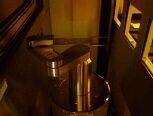
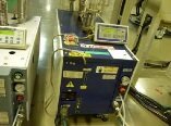
Used AMAT / APPLIED MATERIALS VeraSEM #9196915 for sale
URL successfully copied!
Tap to zoom
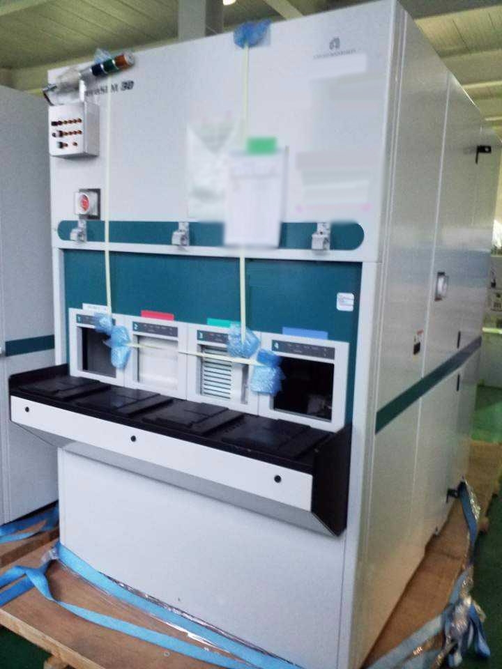

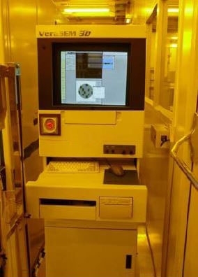

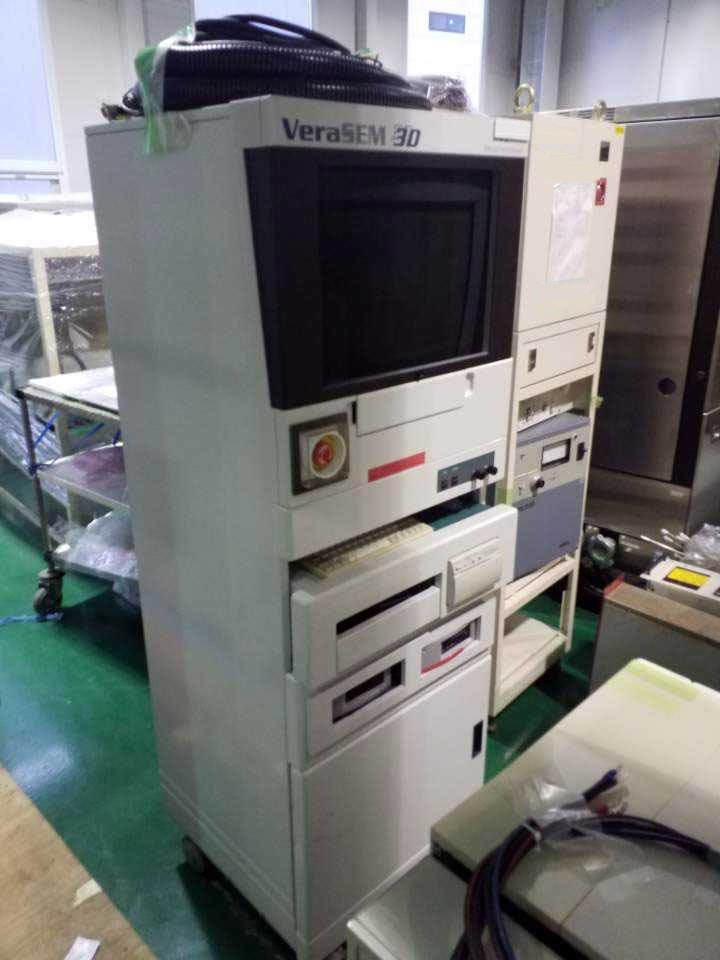

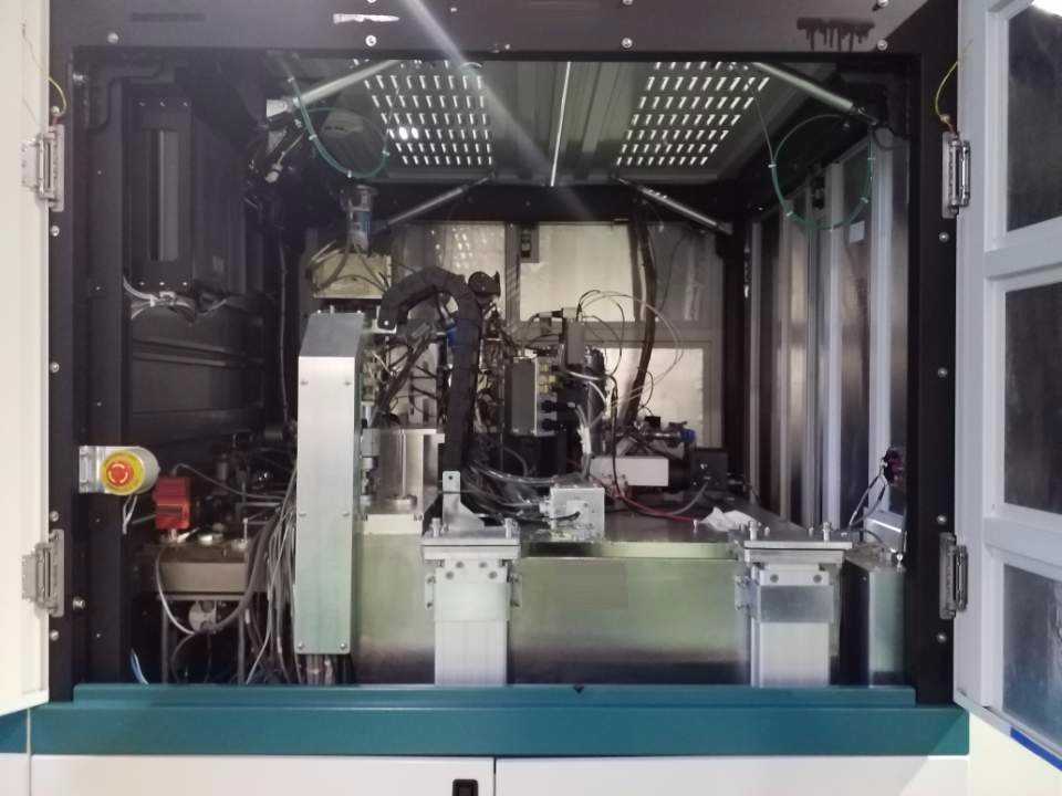

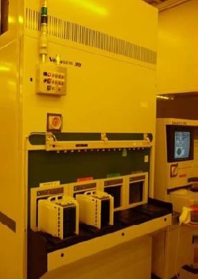








ID: 9196915
Wafer Size: 8"
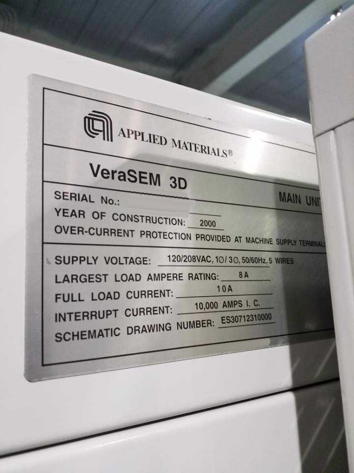
Vintage: 2000
3D Scanning electron microscope (SEM), 8"
Wafer shape: SNNF
PP Miraial, 8"
No SMIF interface
Electron optical system:
Electron gun: Schottky emission source (FEI)
Accelerating voltage: 300V - 2000V
Probe current:
Low: 5pA
Medium: 10pA
High: 20pA
Electromagnetic lens: 3 Stages electromagnetic lens
Boosting voltage: Beam deflector module
Objective lens
Scan coil: 2 Stages electromagnetic deflection (X & Y-axes)
Magnification: 1,000x to 400,000x (100µm to 0.25µm FOV)
Wafer imaging ability: Entire surface of 8" (or 12") wafer
Asspect ratio: >14:1
Tilt function: 5 Degrees (4 Directions)
Resolution: 3nm (500V)
Optical microscope system:
COHU CCD Camera: Monochrome
Magnification: 16x / 220x (450µm / 6000µm FOV)
Wafer imaging ability: Entire surface of 8" (or 12") wafer
Workstation:
Model: SGI Octane
OS: Unix
HDD Capacity: 73 GB
Memory: 1024 MB
SECS/GEM Communication interface
Wafer stages: ANORAD X,Y & Z Stages
Moving speed: 300 mm/sec
Function target: Faraday cup / Resolution target
Wafer transfer:
Wafer shape ability: Notch / Orientation flat
Pre-alignment: Sensing by CCD bar (200/300 mm wafer)
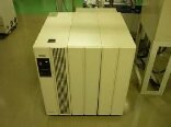
External power distribution unit
Fun filter unit
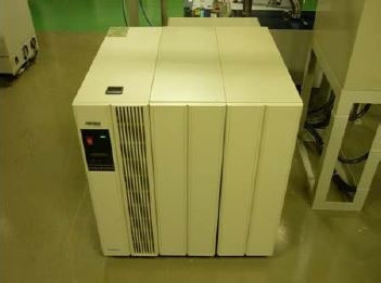
Uninterruptible power supply: POWERWARE+Plus 18/18
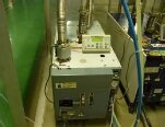
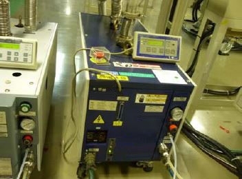
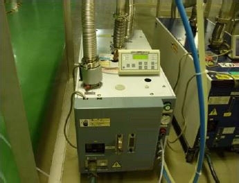
Dry pump load lock: EBARA AA20
Dry pump chamber: EBARA A10S
2000 vintage.
AMAT / APPLIED MATERIALS VeraSEM is an advanced wafer testing and metrology equipment that provides the highest level of accuracy, precision and throughput. AMAT VeraSEM's robust, flexible and powerful platform allow for integrated solutions to improve the quality, productivity and yield of wafer testing. APPLIED MATERIALS VeraSEM is an integrated system that is composed of four primary components: the scanner and sample stage, an advanced wafer inspection unit, an optical inspection and focus sensing machine, and a laser tool. VeraSEM's scanner and sample stage are designed to provide precise, repeatable scan and sample positioning to ensure maximum test efficiency. The asset features excellent repeatability and stability, preserving the same scan and sample positions for multiple operations. The advanced wafer inspection model of AMAT / APPLIED MATERIALS VeraSEM utilizes advanced light sources, specialized filters and sensors to quickly identify weak spots, bubbles, scratches and other defects in the wafer. The equipment can also accurately measure wafer thickness, flatness and tilt. The optical inspection and focus sensing system allows for high accuracy surface and backside inspections to detect issues that can have an impact on the production process. This unit is also capable of measuring and tracking small defects, providing a comprehensive view of the wafer's condition. Finally, the laser machine is used to accurately measure wafer profile, IPE, EPE, and Zernike analysis. It also provides precise measurements to detect particles, pits, and more. AMAT VeraSEM is the perfect choice for any business looking for an all-in-one solution to test, measure, and inspect a wide range of wafer sizes. The tool's precise and repeatable scanning, advanced wafer inspection, optical inspection and focus sensing, and laser systems make it a powerful tool for wafer testing and metrology.
There are no reviews yet


