Used FEI DA300 #293670288 for sale
URL successfully copied!
Tap to zoom



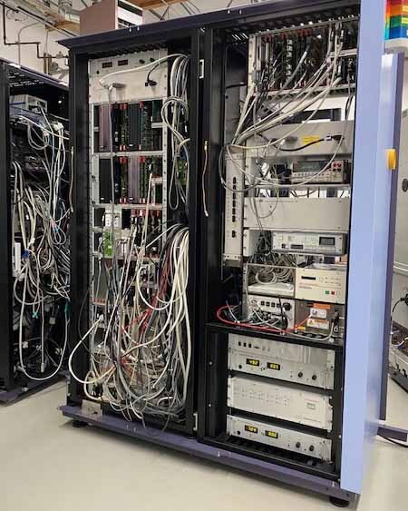


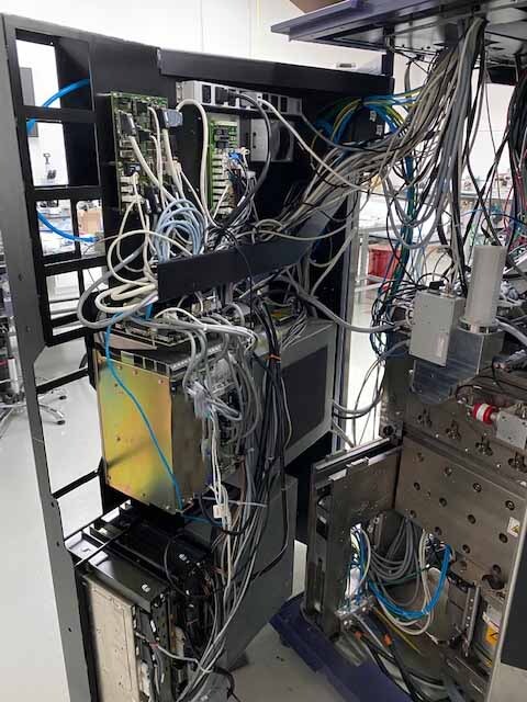

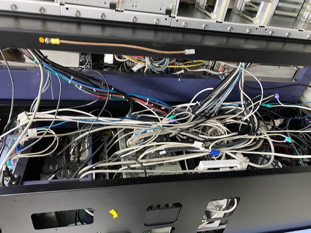

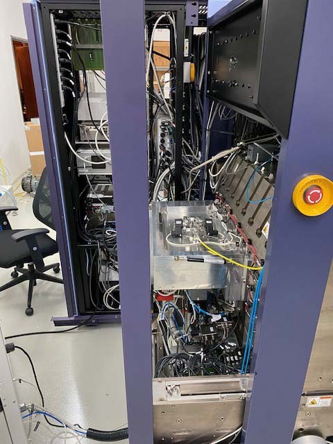



ID: 293670288
Wafer Size: 12"
Vintage: 2010
Defect analyzer, 12"
NG Scanning Electron Microscope column (SEM)
Detectors: ETD, TLD, CDEM
Sidewinder FIB Column: 20 nA
BROOKS Front end FOUP
Capacitance probe
OXFORD 30 mm
SDD EDS
Plasma cleaner
OMNIPROBE 200 Manipulator
Gas injection system: Pt
Operating system: Windows XP
2010 vintage.
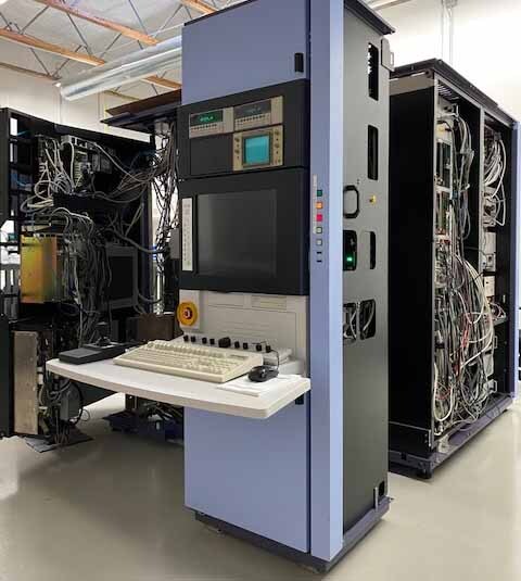
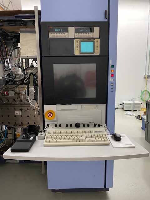
FEI DA300 is a high-performance wafer testing and metrology equipment designed to handle the most demanding of test scenarios. The flexible system is ideal for testing thick and thin wafers, and is capable of handling a variety of tasks across a range of semiconductor technologies. DA300 unit comprises a high-precision interferometer and a protective chamber, as well as several wafer test stages for various wafer sizes and configurations. The interferometer, which is designed to measure surface flatness and differences in height, operates under a closed-loop machine that enables faster computation. Additionally, a dedicated high-end motion control tool ensures superior accuracy and fine traceability, allowing for precision in testing. In terms of optics, the asset utilizes an imaging model with a 4-inch MIMO aperture, and a fully-programmable continuous mechanical scan mode. The equipment also features advanced software with a range of advanced algorithms for both two-dimensional and three-dimensional wafer testing. What's more, the system is also capable of handling a range of optional weighing capabilities, allowing for faster inspections as well as heavier workloads. FEI DA300 is designed to be intuitive and easy to use, providing clear early warning signs for potential issues. It also features an integrated control unit with color touch screens, which allow users to quickly access the most frequently used parameters at the press of a button. The machine also provides on-the-fly measurements and automated report generation features, allowing for a more efficient workflow. Overall, DA300 is a powerful and reliable wafer testing and metrology tool that is designed to handle a variety of tasks, from precision surface flatness and height measurements to automatic on-the-fly measurements. The asset is also optimized for performing heavy workloads quickly and accurately, while the software provides a wide range of advanced features to allow users to get the most from the model.
There are no reviews yet
