Used KLA / TENCOR 6420 Surfscan #293767210 for sale
URL successfully copied!
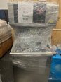
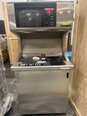
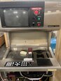
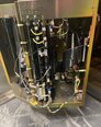
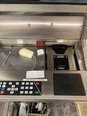
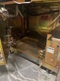
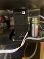
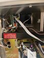
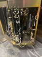
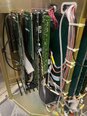
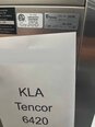
Tap to zoom
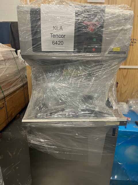

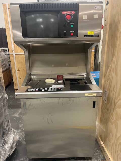
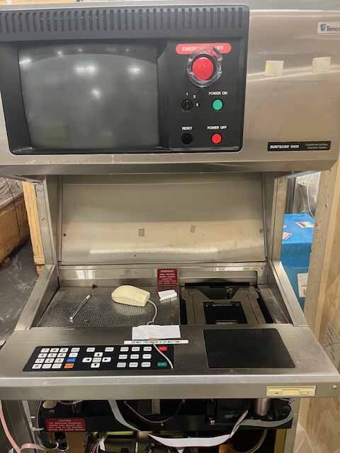
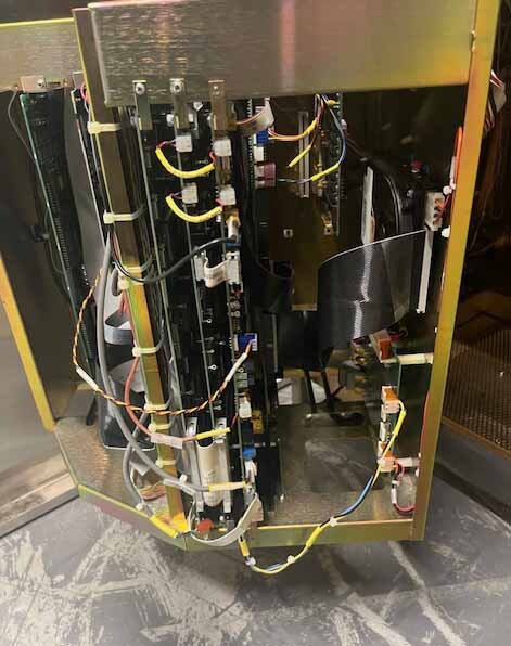
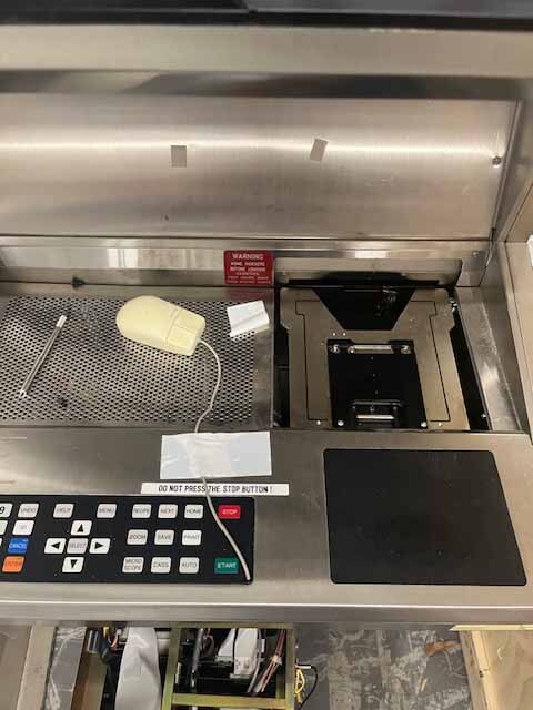
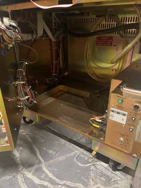
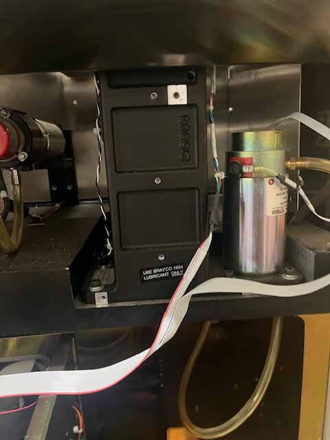
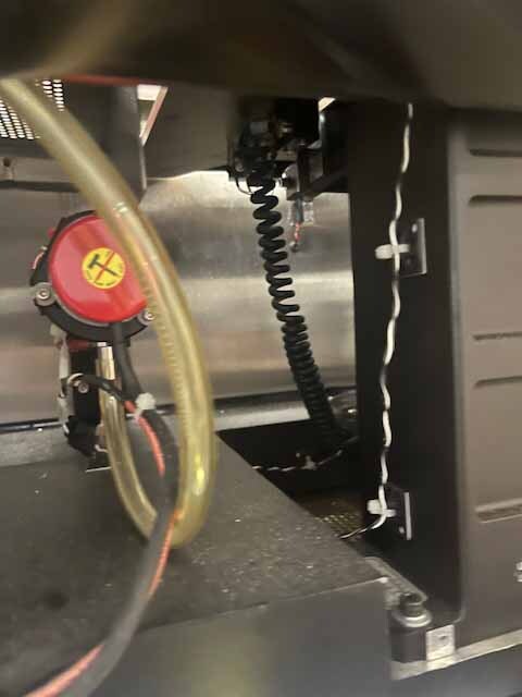
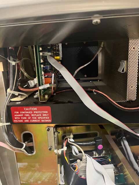
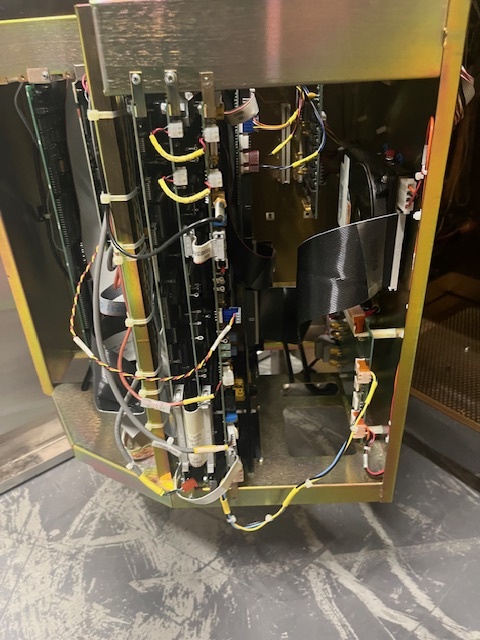
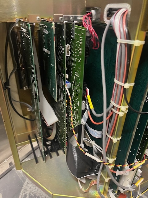
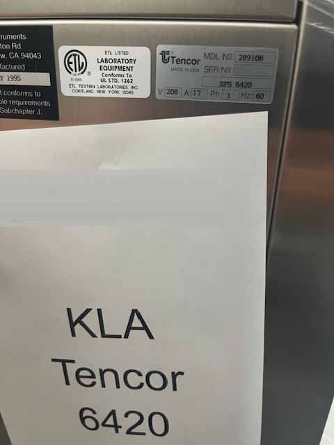
ID: 293767210
Wafer Size: 8"
Vintage: 1995
Automatic surface inspection system, 8"
1995 vintage.
KLA / TENCOR 6420 Surfscan is a Wafer Testing and Metrology Equipment designed for use in the semiconductor industry. It is capable of testing and measuring both optical and electrical properties of wafers, and providing accurate and repeatable data for analysis. The SurfScan 6420 is equipped with two main components - a WaferOptics™ laser optics scanning stage, and a Scanpath™ scanning controller. The WaferOptics™ is a high speed, stable, and linear scanning stage designed to accurately and repeatably measure surface topological data. Its encoder resolution is 0.15 micron with a repeatability of ±0.01 micron per axis. The Scanpath™ scanning controller contains the proprietary algorithms to interpret the surface profile data and convert it into meaningful metrics. This system is capable of producing metrics such as non-uniformity maps, performance maps, overlay results, and other wafer surface data. The unit also includes several additional components, such as a Zoom Optics™ module, which provides an extended range of view of low voltage signals. An advanced OPC machine, originally developed for use with KLA 193nm and 248nm systems, is also included, allowing precise overlay calibration and feature alignment. The tool operates in "head-in-hand" mode, which means that measurements can be taken while the wafer remains mounted in the asset, allowing users to take multiple measurements on the same wafer with no loss of positioning or time. In terms of hardware and software, KLA 6420 Surfscan is equipped with a Pentium 4 processor, Windows 7 operating model, a dual-head graphics card, 16GB of RAM and a 32GB hard drive. The device also includes an Ethernet connection for remote access and communication with other TENCOR systems. The device is compatible with various types of customer software and interfaces for analysis and automation. Finally, TENCOR 6420 Surfscan is fully capable of quantitative defect detection and overlay metrology. Utilizing advanced defect metrology algorithms and optical imaging, the equipment is able to detect and classify defects with greater sensitivity and accuracy. This brings more information to the user than traditional imaging and wafer testing systems, allowing them to make better, more efficient decisions that can affect their bottom line.
There are no reviews yet