Used KLA / TENCOR / THERMA-WAVE 18-016170 #293751425 for sale
URL successfully copied!
Tap to zoom
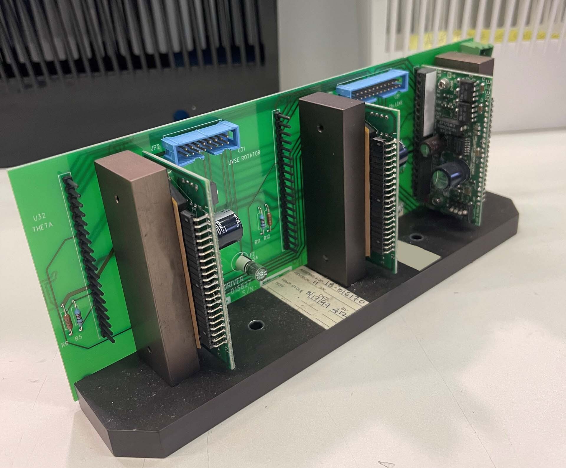

KLA / TENCOR / THERMA-WAVE 18-016170 is a sophisticated wafer testing and metrology equipment that has been designed to meet the demands of the semiconductor industry for high precision and accuracy in measuring thin film properties and material characteristics on semiconductor wafers. This state-of-the-art system combines advanced optical and thermal techniques to deliver comprehensive wafer analysis capabilities that are essential for ensuring the quality and performance of modern semiconductor devices. KLA 18-016170 unit is equipped with a range of advanced features and functionalities that make it a powerful tool for characterizing the properties of thin films on semiconductor wafers. The machine employs a combination of spectroscopic ellipsometry, reflectometry, and infrared measurements to accurately determine critical parameters such as film thickness, refractive index, and optical constants with high precision and resolution. One of the key strengths of TENCOR 18-016170 tool is its ability to perform non-destructive and contactless measurements on a wide range of materials, including silicon, compound semiconductors, metals, and dielectrics. This flexibility makes the asset suitable for a variety of applications in the semiconductor industry, from process development and optimization to quality control and failure analysis. The model's advanced software algorithms and data analysis tools enable users to extract valuable information from the measurement data, allowing for detailed characterization of the properties of thin films and the identification of potential process issues or defects. The equipment also offers customizable measurement recipes and automated data acquisition capabilities, streamlining the measurement process and improving productivity in the wafer analysis workflow. In addition to its wafer testing capabilities, THERMA-WAVE 18-016170 system is also equipped with advanced metrology features that allow for the characterization of wafer topography, surface roughness, and other critical parameters that are essential for optimizing semiconductor processing and ensuring the quality of the final semiconductor devices. Overall, 18-016170 unit represents a cutting-edge solution for wafer testing and metrology in the semiconductor industry. With its advanced optical and thermal measurement techniques, powerful data analysis capabilities, and flexible measurement configurations, the machine offers semiconductor manufacturers a comprehensive tool for achieving the highest level of quality control and process optimization in semiconductor device manufacturing.
There are no reviews yet