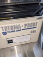
Used KLA / TENCOR / THERMA-WAVE TP 500 #293824688 for sale
URL successfully copied!
Tap to zoom
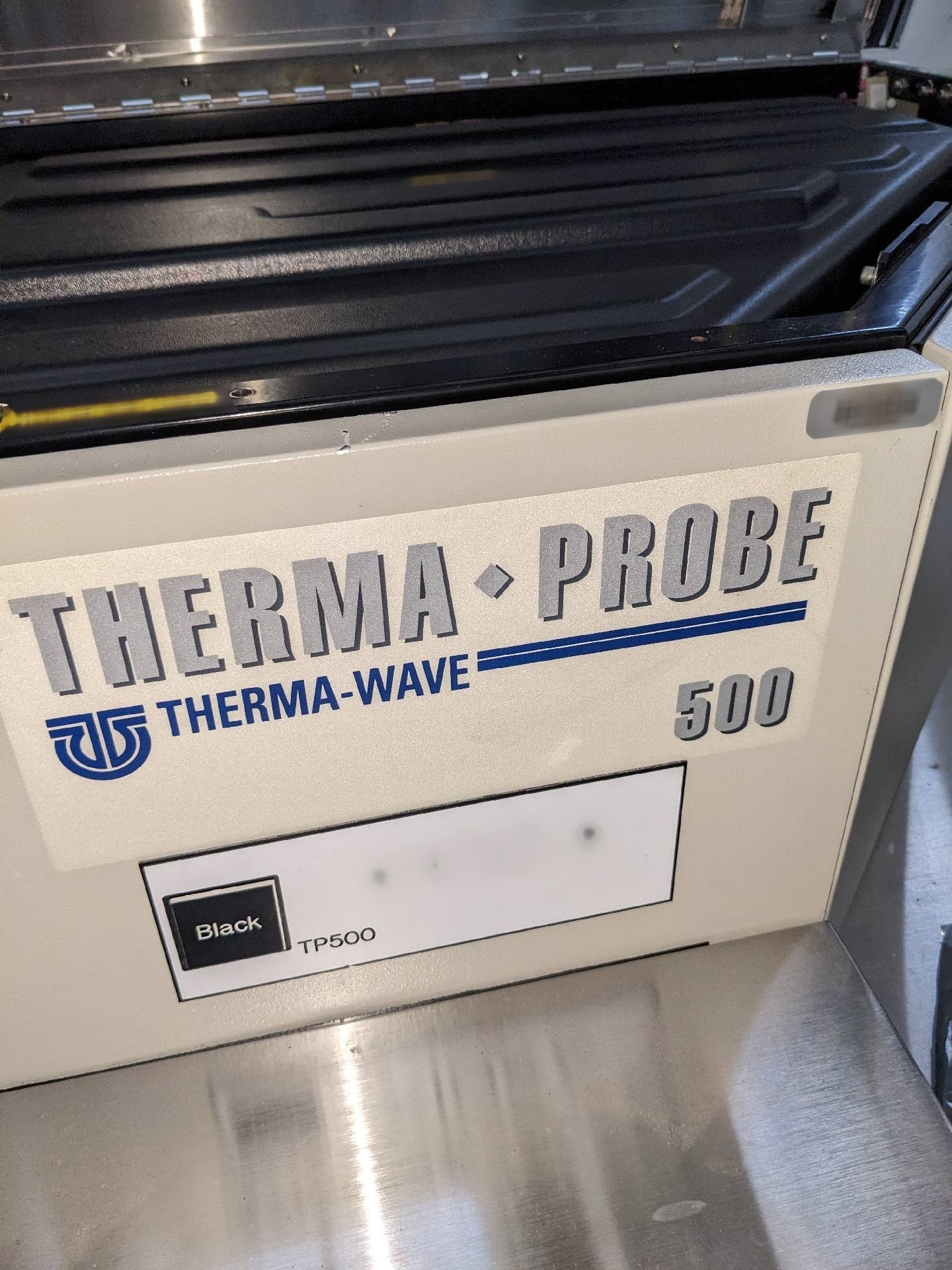

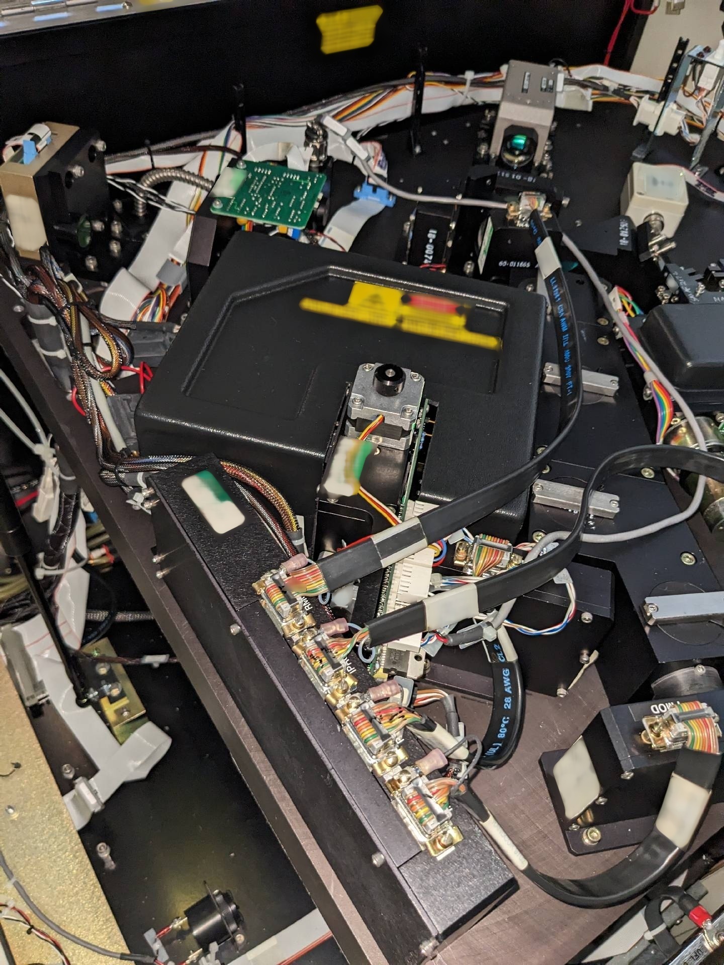
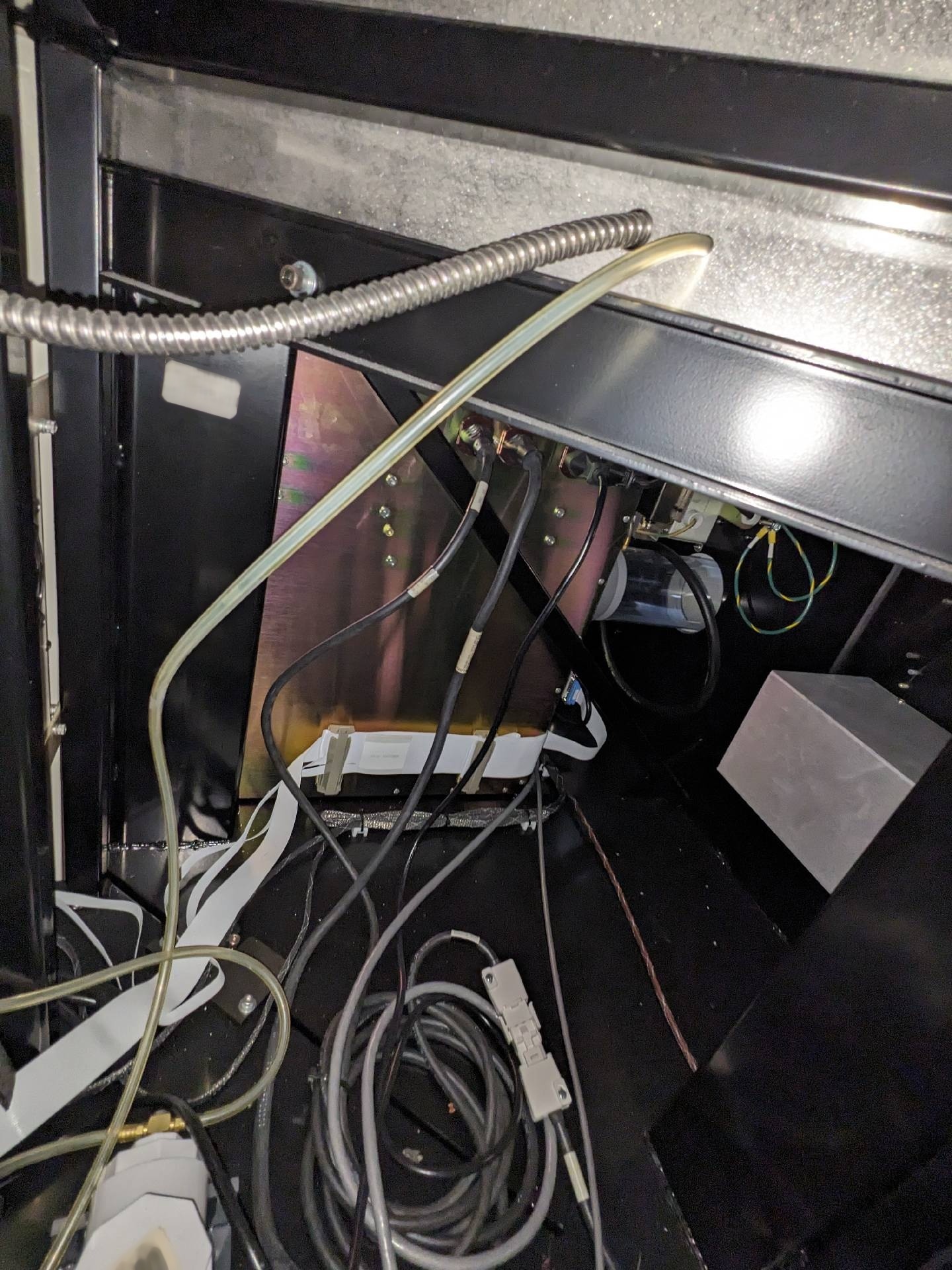
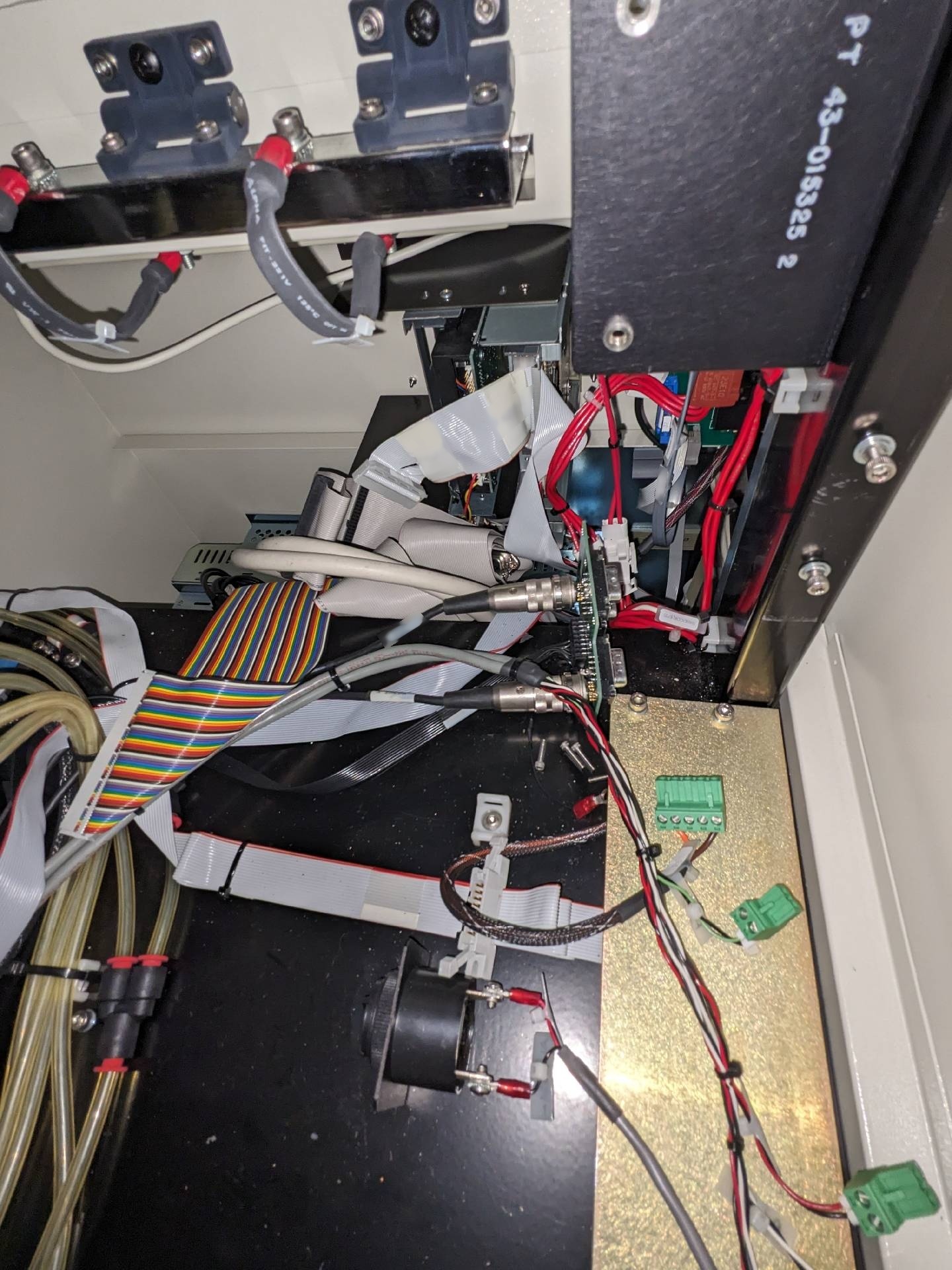
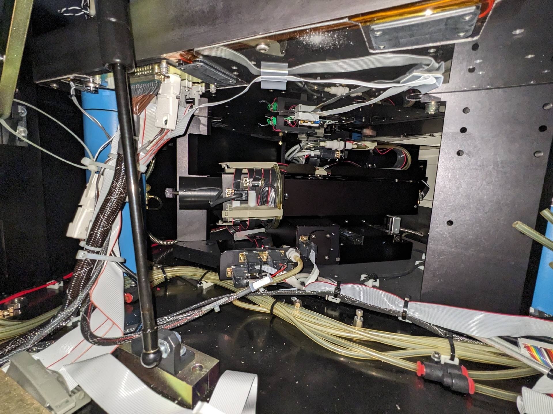
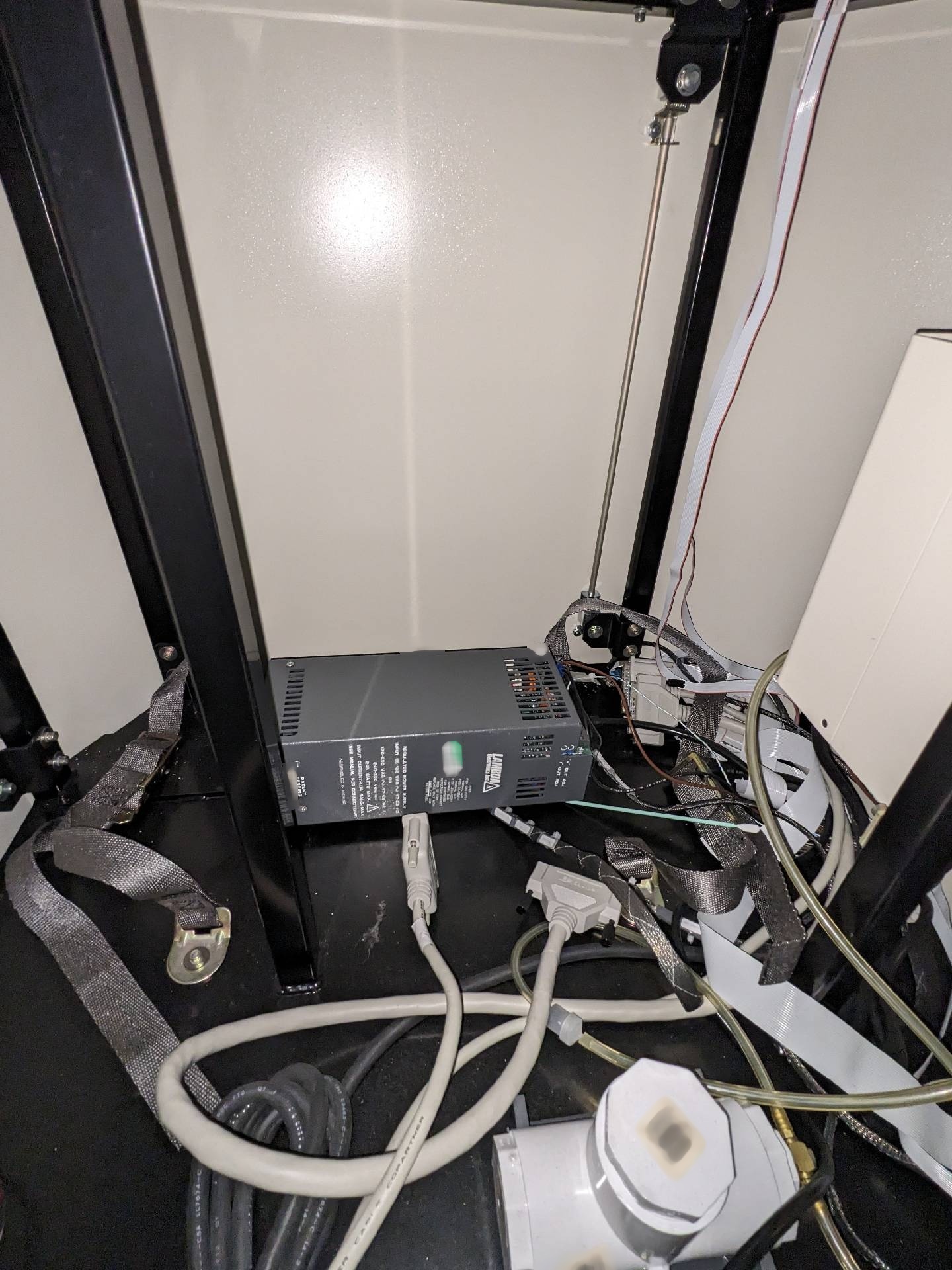
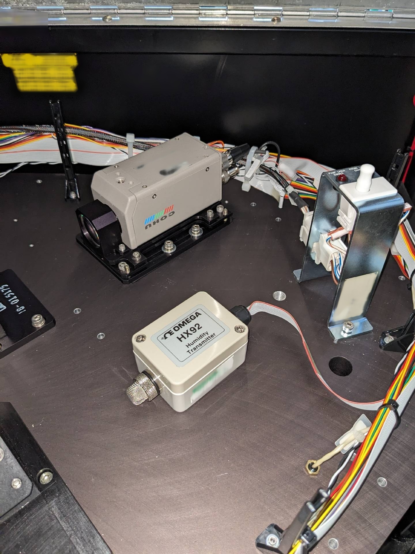
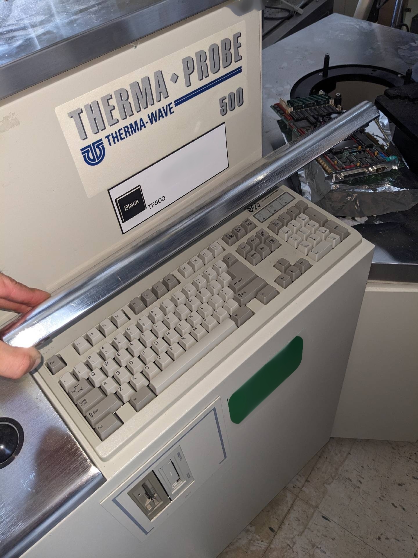
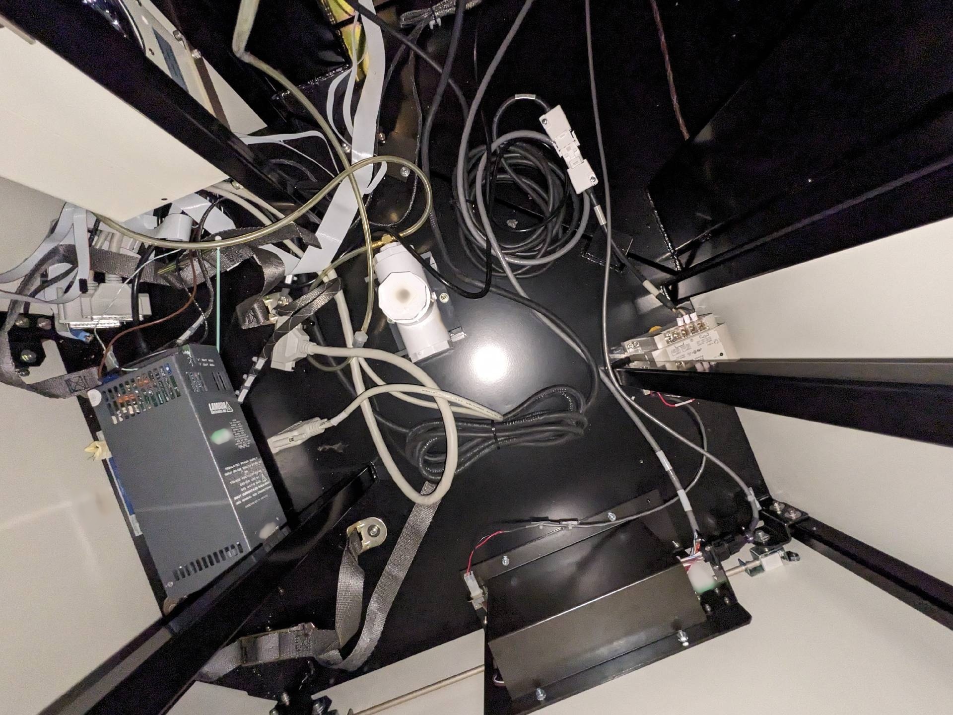
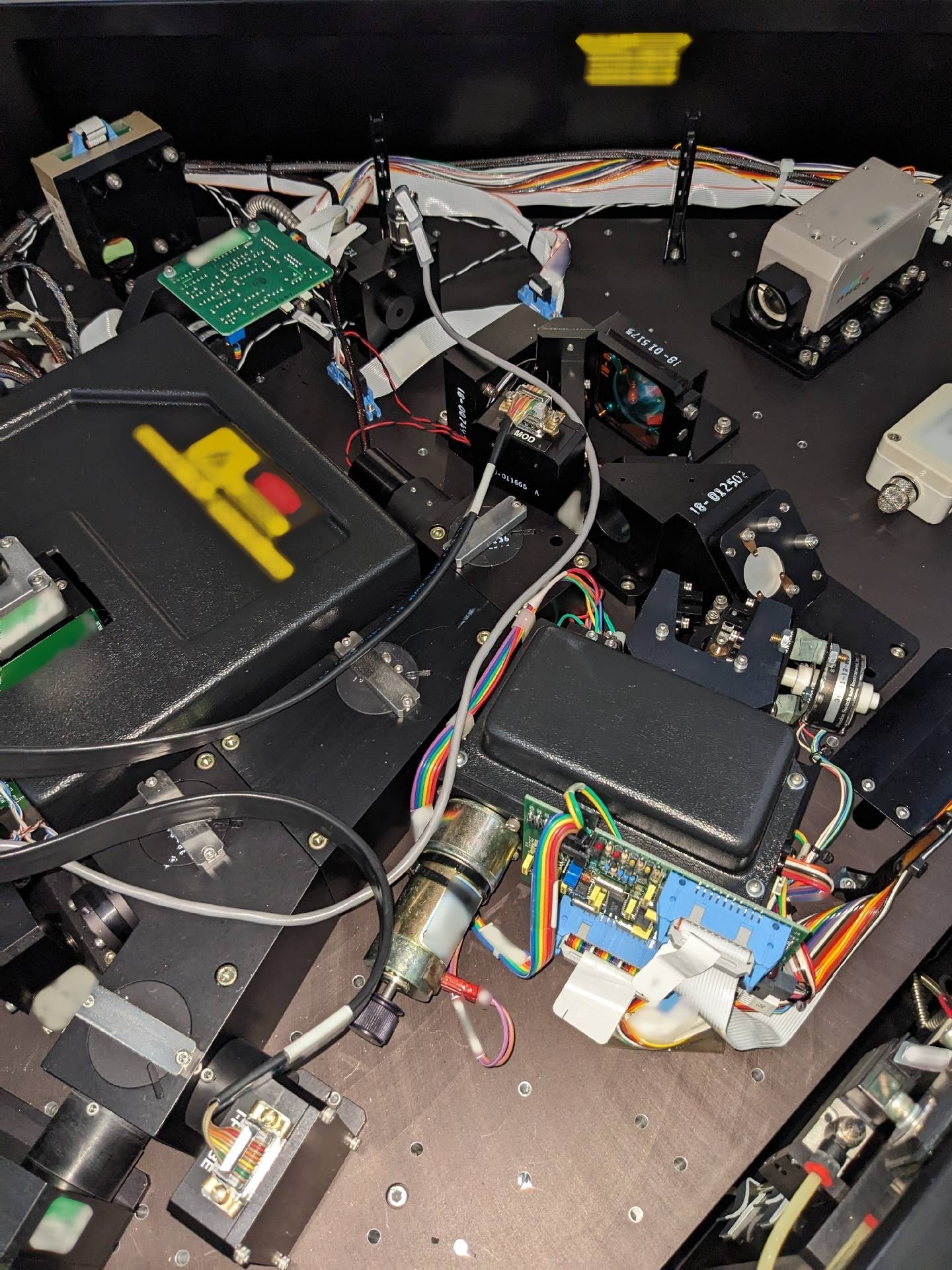
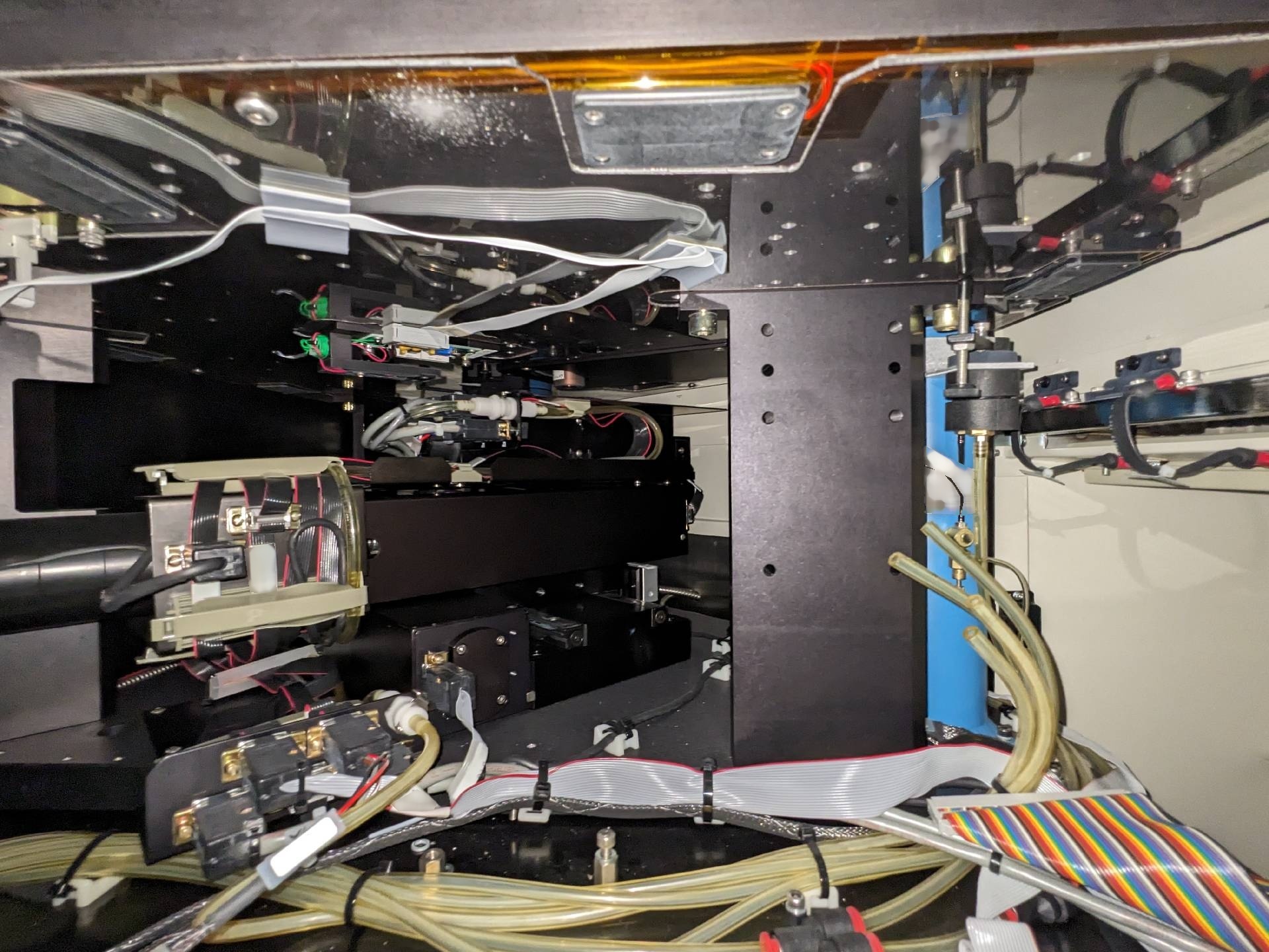
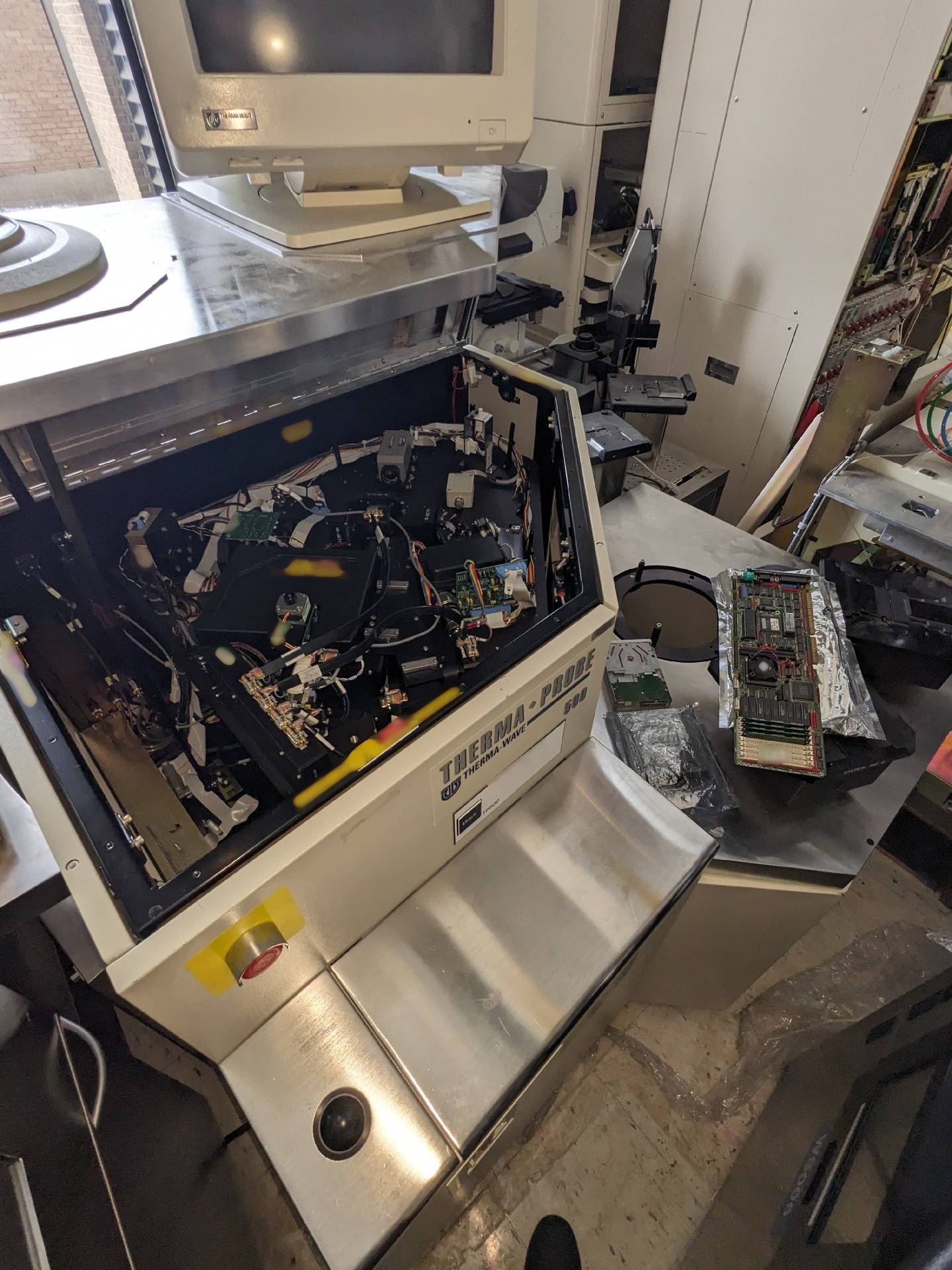
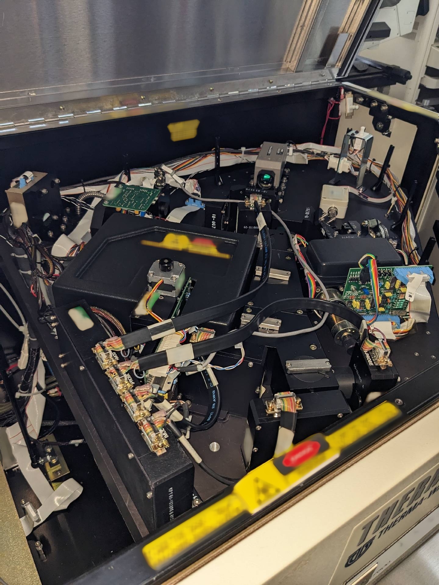
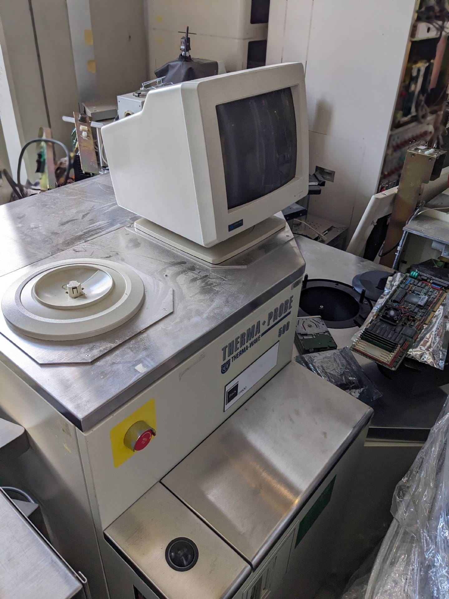
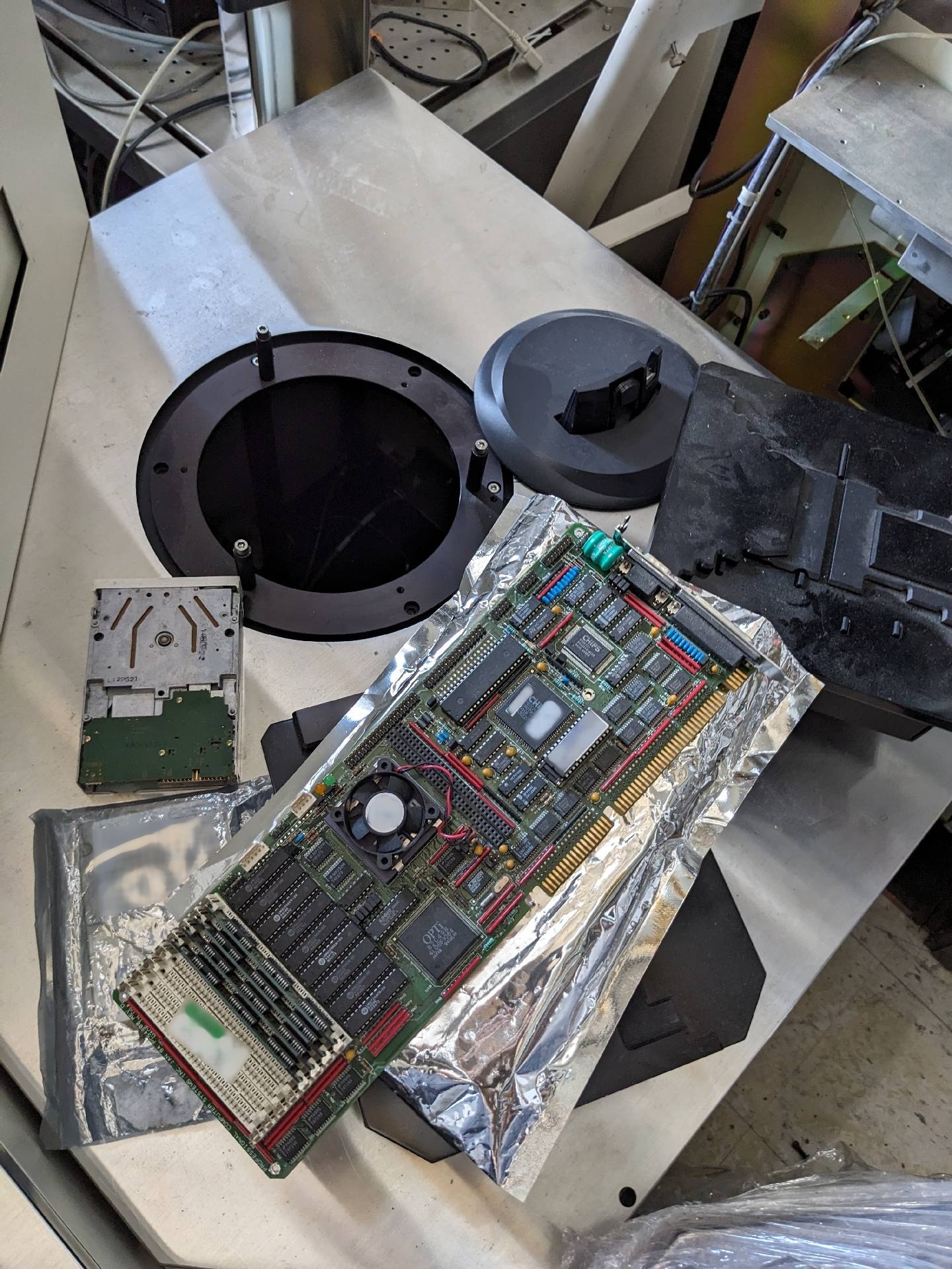
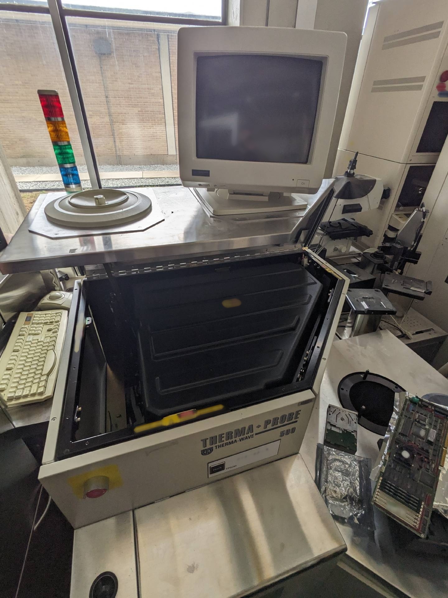
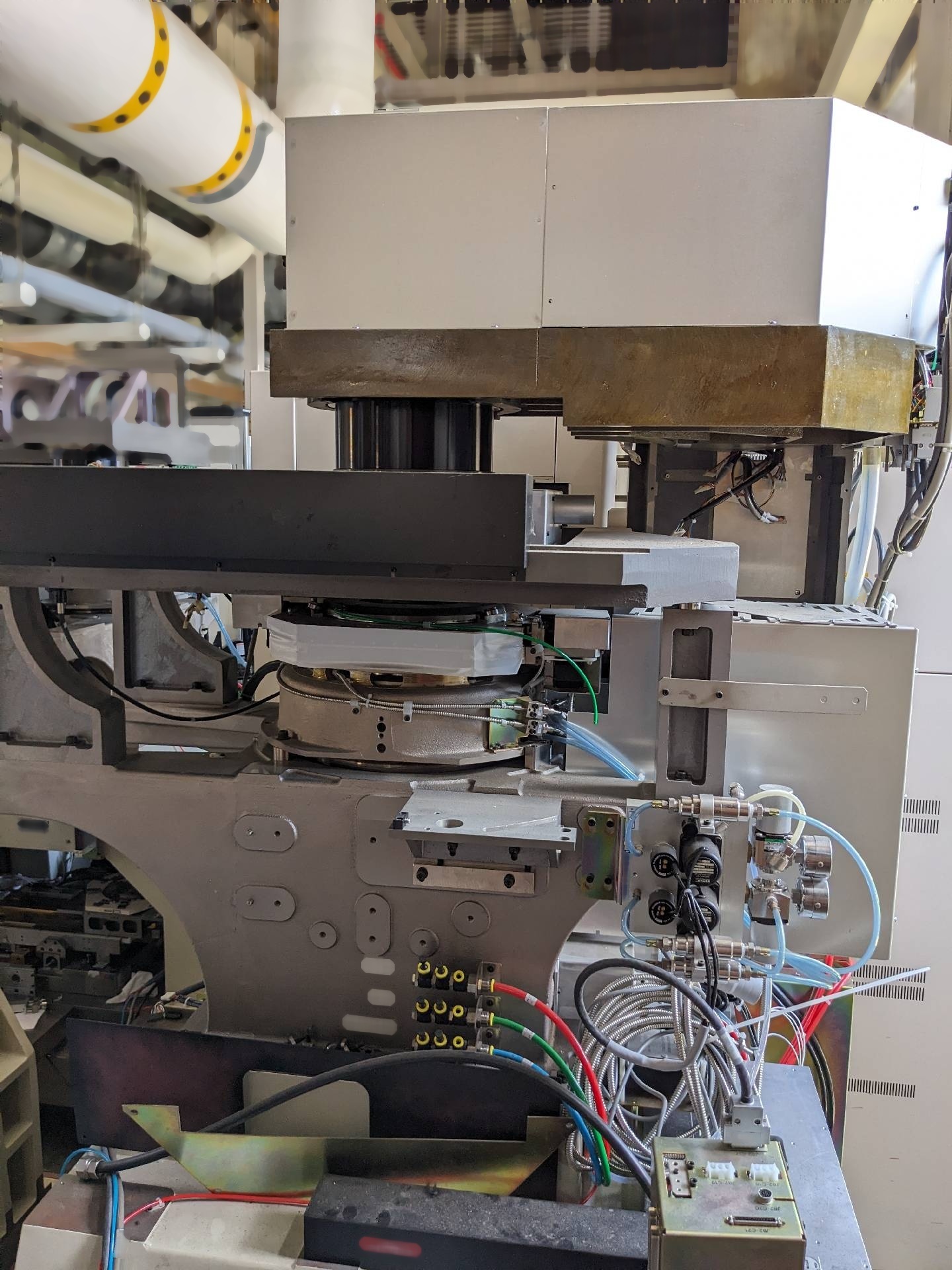
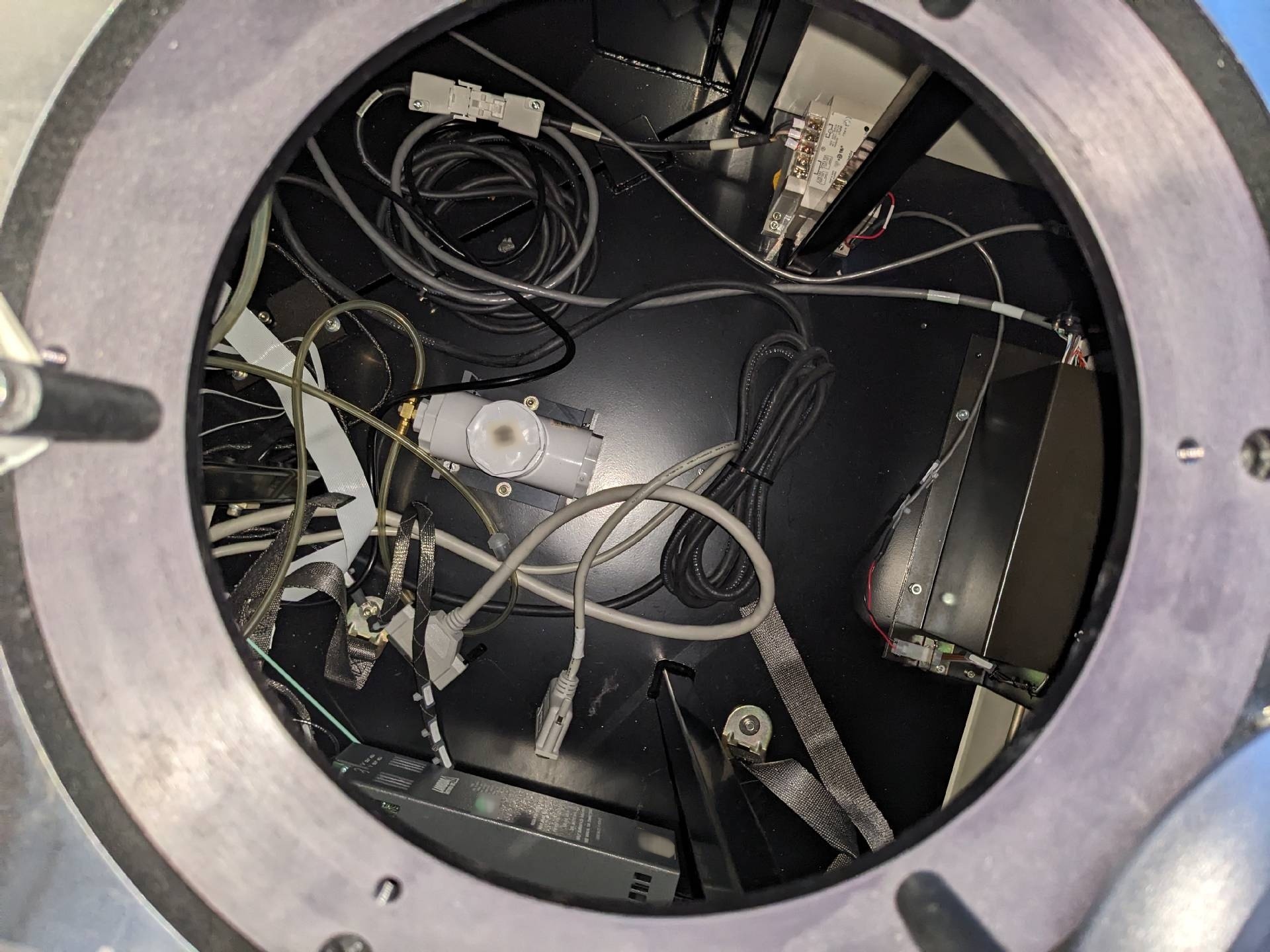
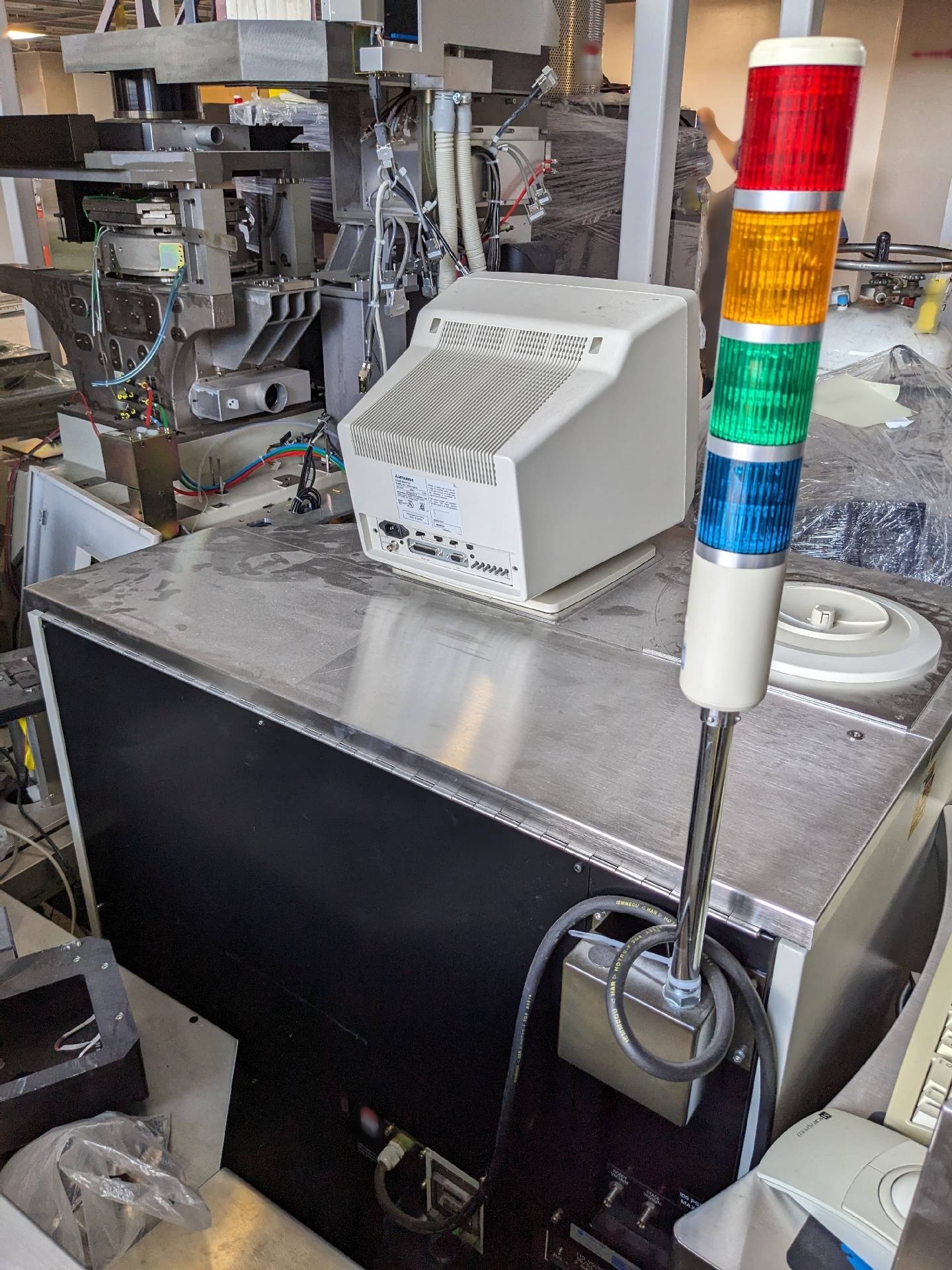
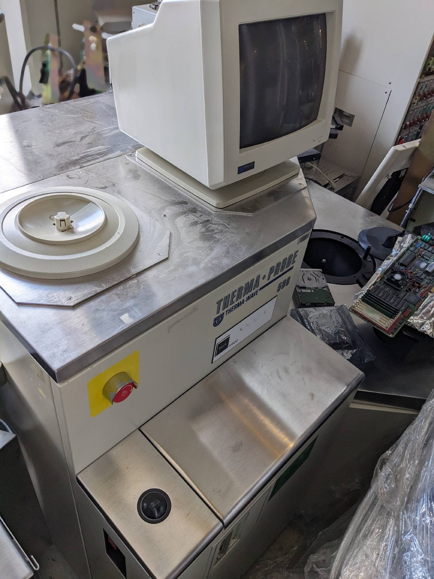
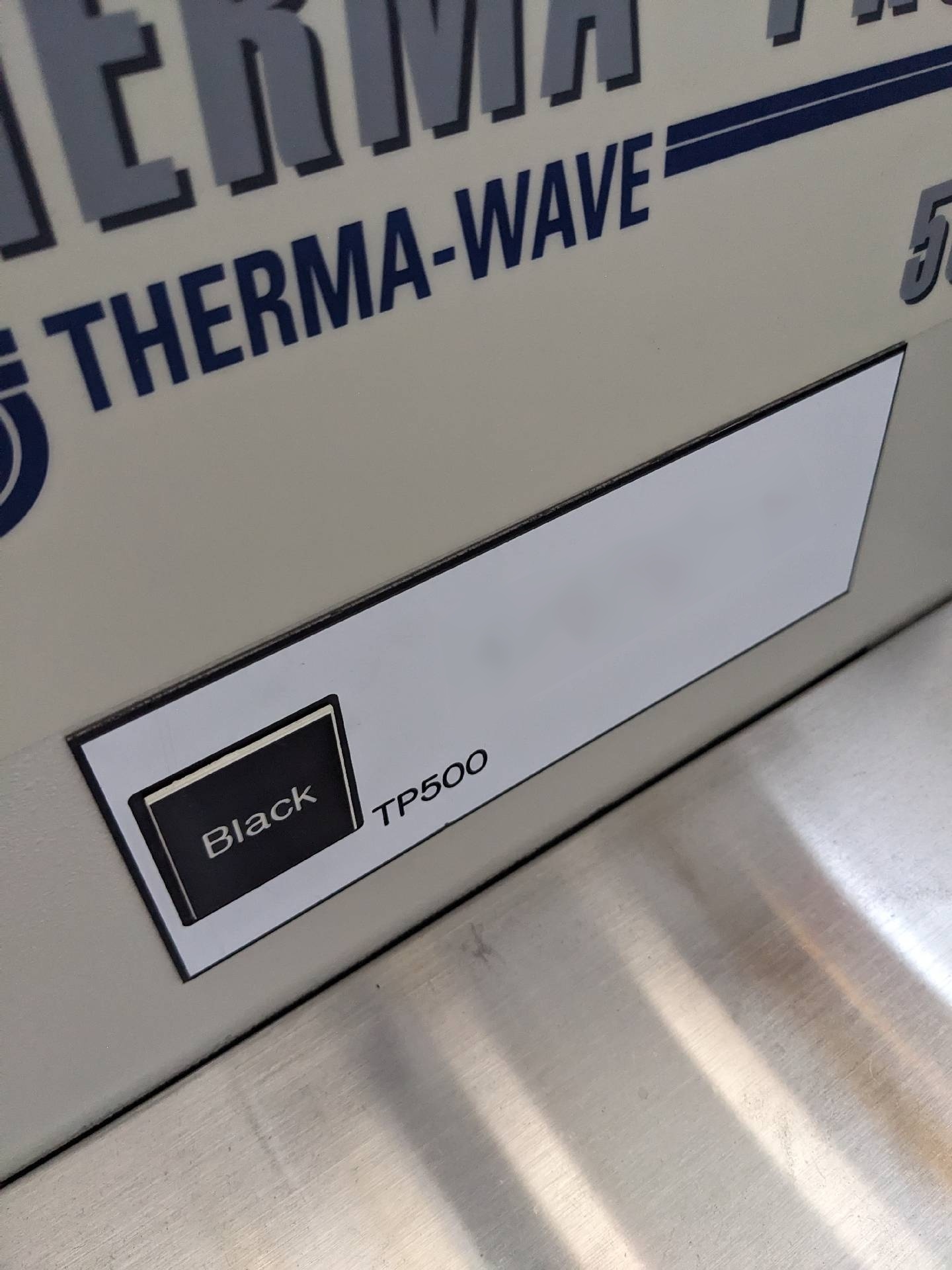
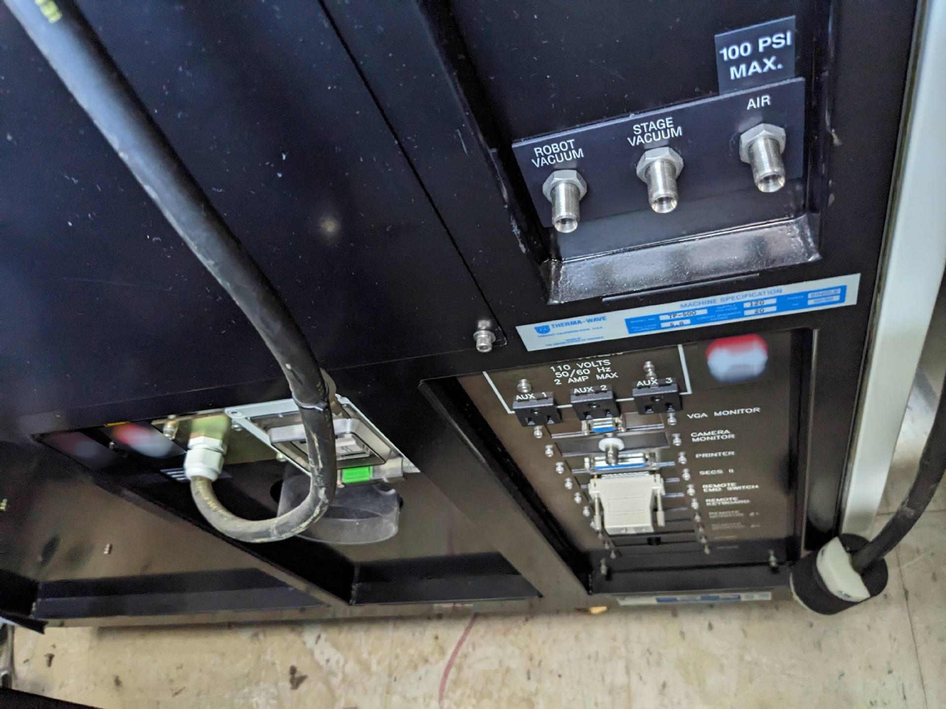
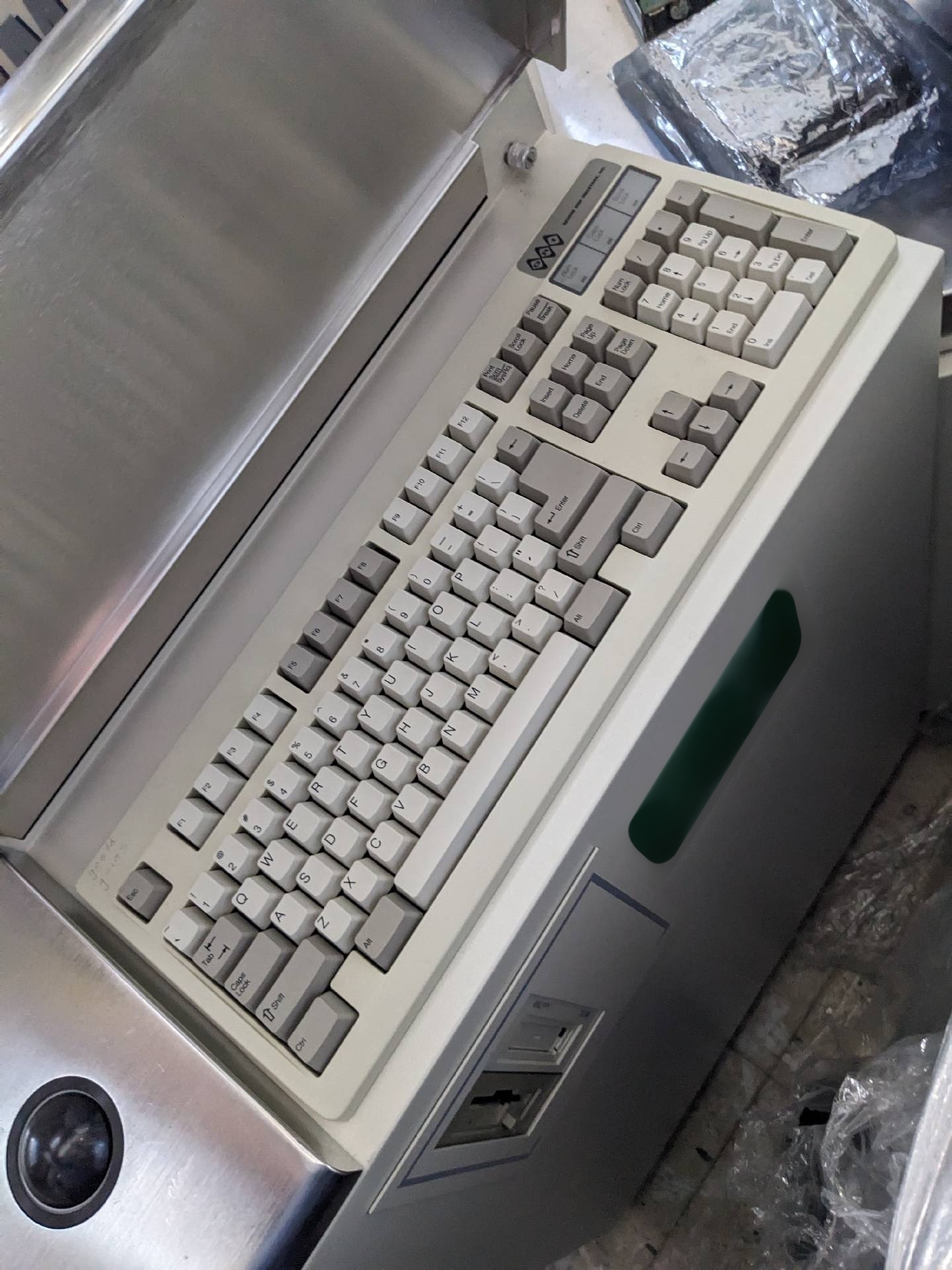
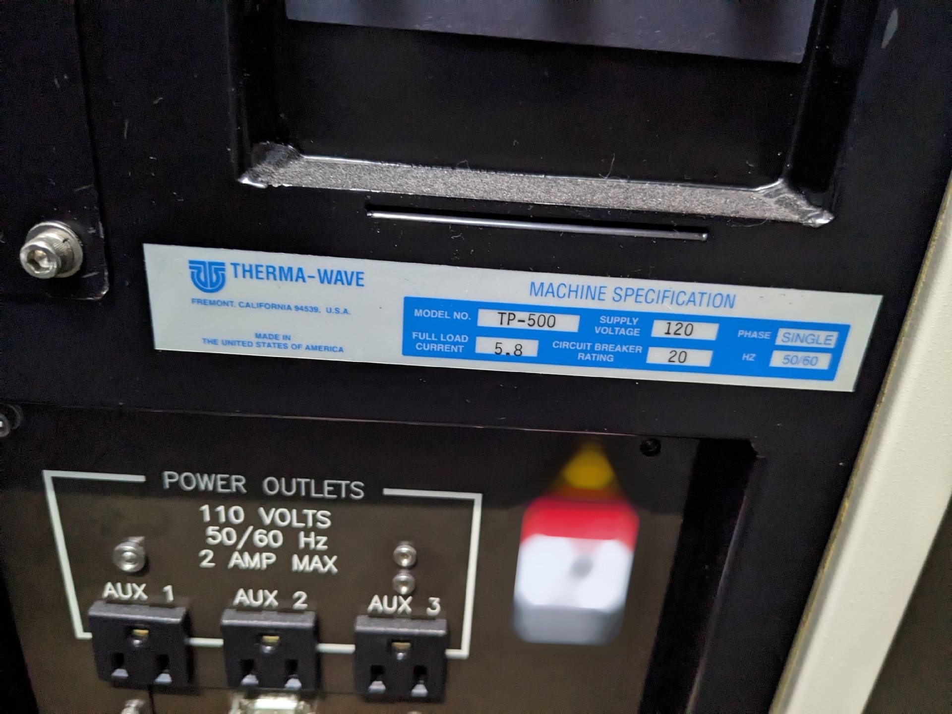
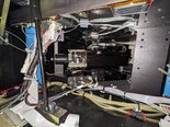
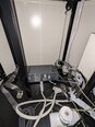
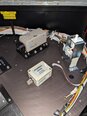
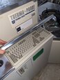
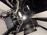
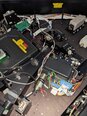
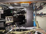
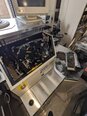
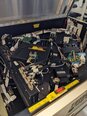
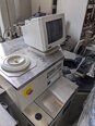
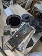
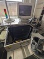
KLA / TENCOR / THERMA-WAVE TP 500 is a wafer testing and metrology equipment that offers accurate, reliable pre-process and post-process characterization for process/product validation, verification and refinement. The system features a high-precision optical stitching engine and an automated overall scanning function for accurate, rapid wafer mapping. KLA TP 500 offers an easy-to-use, stand-alone design with a single click two-dimensional (2D) automated focus unit. It is equipped with a suite of integrated process control software for real-time analysis and control of each process parameters to ensure repeatable performance. In order to optimally inspect and characterize advanced semiconductor devices, the machine incorporates a wide range of technology specific tools such as optical defect detection, scattering, topography and overlay alignment. Its optical measurement equipment creates detailed process-specific images and maps of wafers while its scanning electron microscope (SEM) releases high-resolution metrology images. TENCOR TP-500 is also highly automated, enabling cost-efficiencies and ease-of-operation. It allows users to quickly analyze large quantities of data and adjusts parameters using its automated control tool. In addition, the asset's scan time ensures that a large number of wafers can be inspected and tested in a single day, thereby saving time and resources. TP 500 also features cutting-edge, advanced wafer testing and characterization technology. Its cutting-edge algorithms accurately identify and classify particles and defects, leading to improved yield and better process results for subsequent lithography, etch or deposition processes. Finally, the model comes with a user-friendly interface, and its automated functions greatly reduce manual operations, thereby reducing human errors and overall costs associated with the process. In conclusion, KLA TP-500 provides a reliable, efficient and cost-effective wafer testing and metrology solution. Its cutting-edge technology helps identify and classify particles and defects while its automated operation and functionality helps save time, effort, and money. The equipment's advanced characterization capabilities are essential for ensuring optimal device design, ensuring cost-efficiency, and increasing yields.
There are no reviews yet