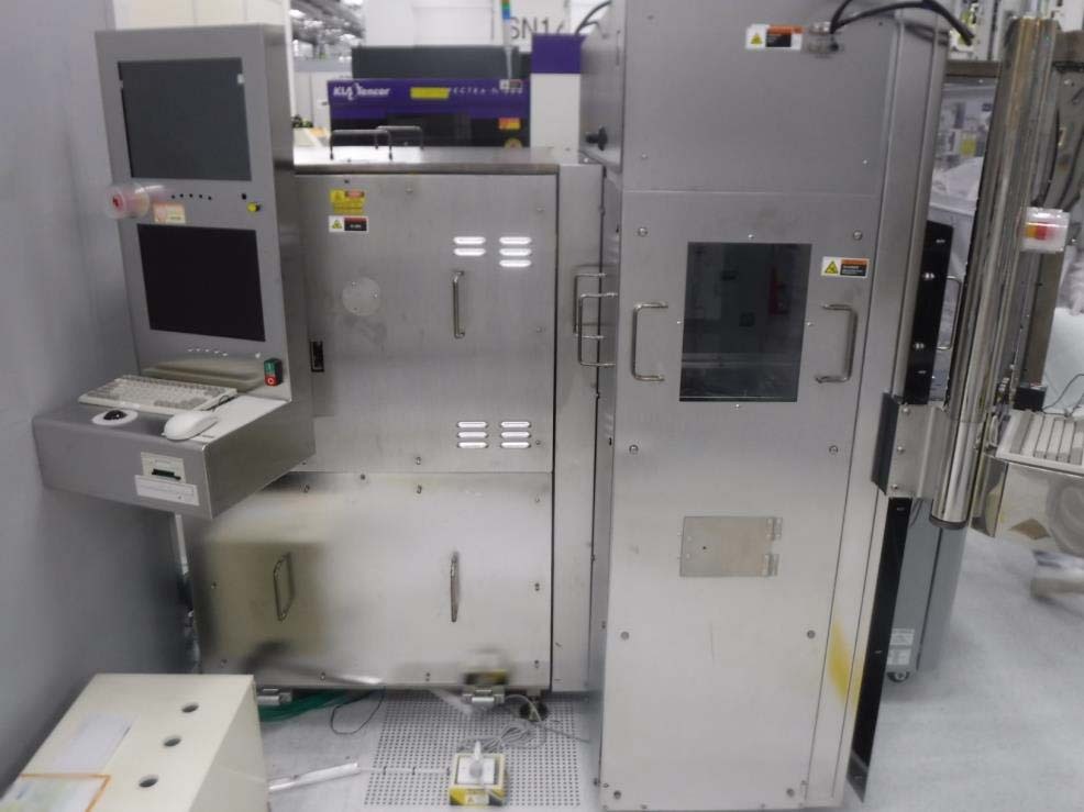
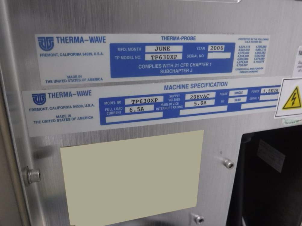
Used KLA / TENCOR / THERMA-WAVE TP 630XP #293759748 for sale
URL successfully copied!
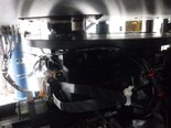

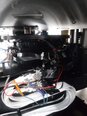
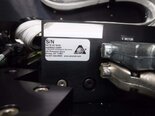
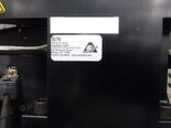
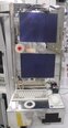
Tap to zoom

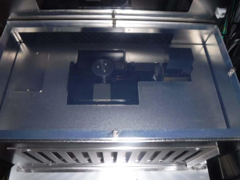
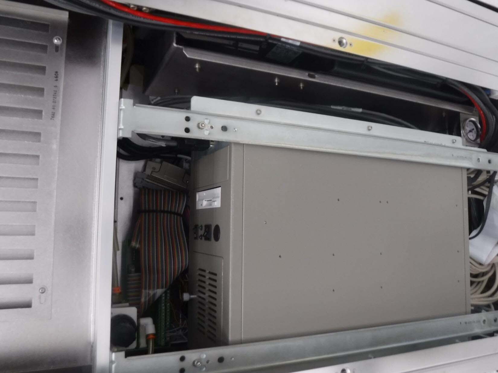
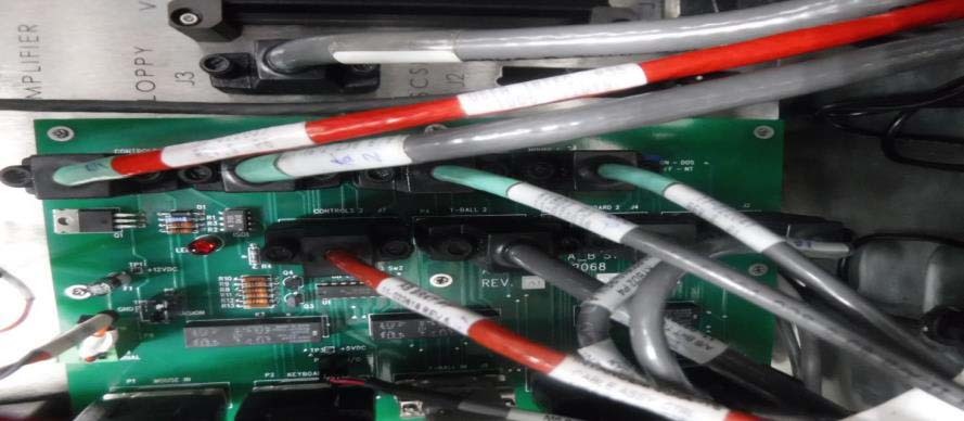
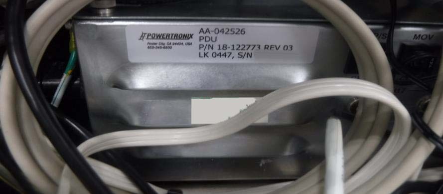
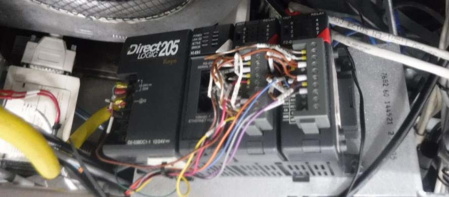
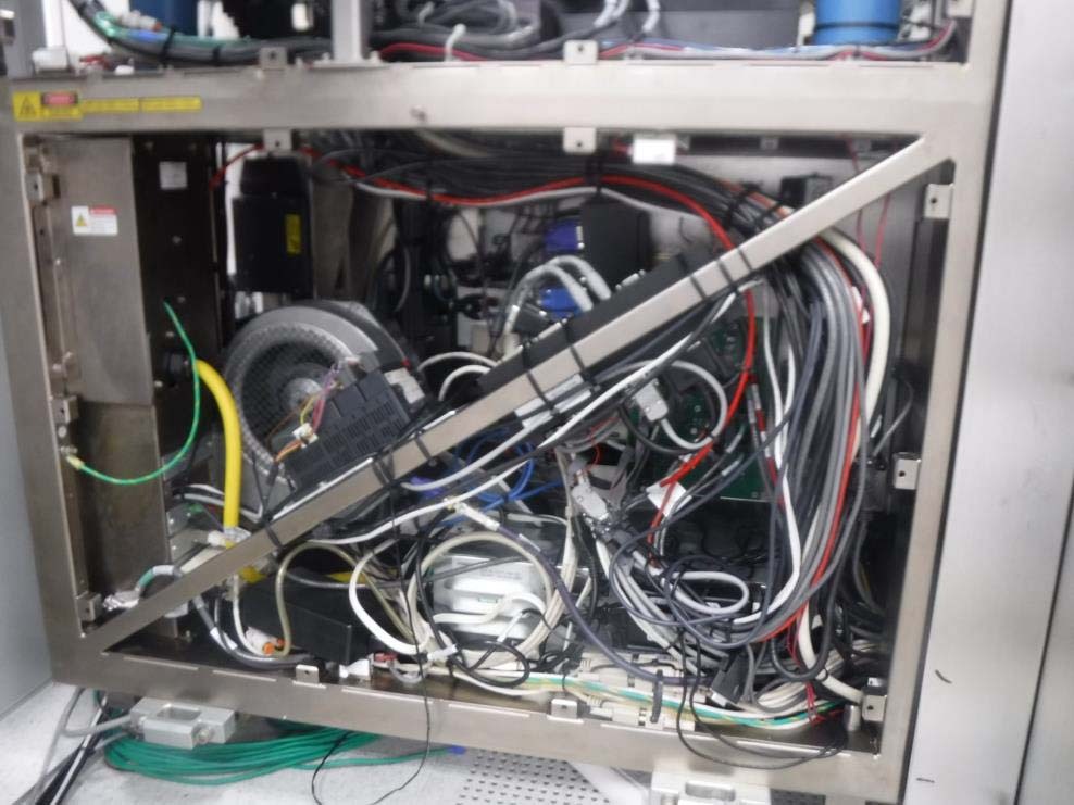
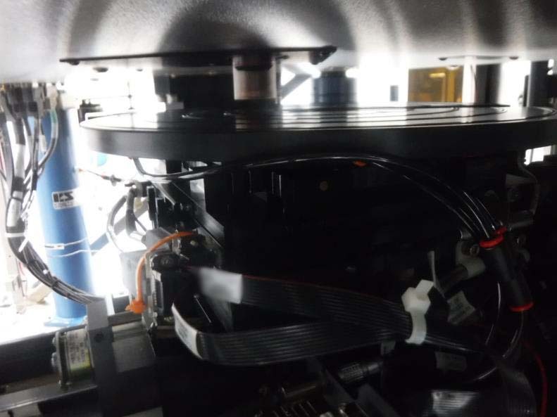

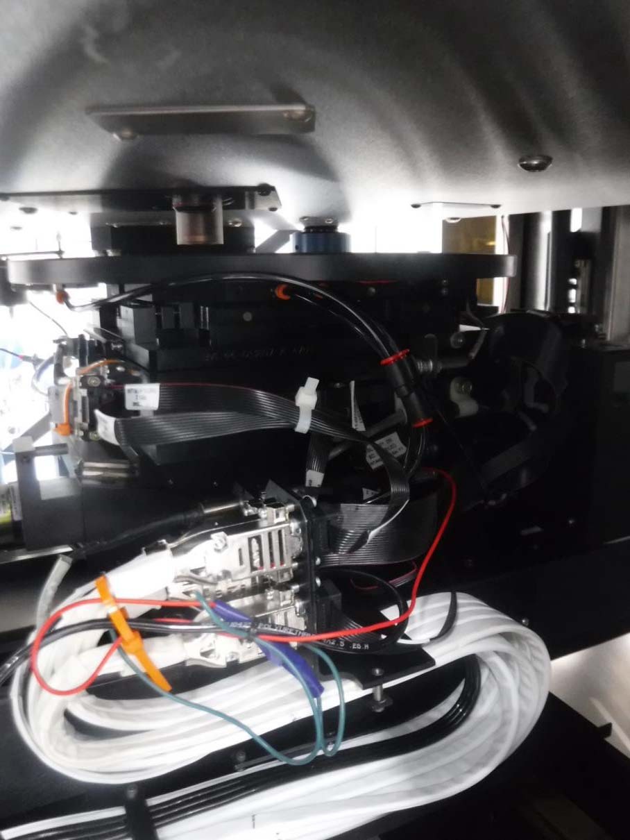
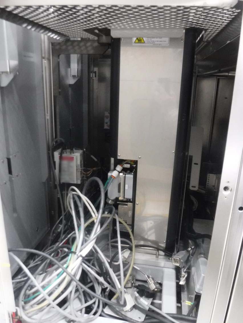
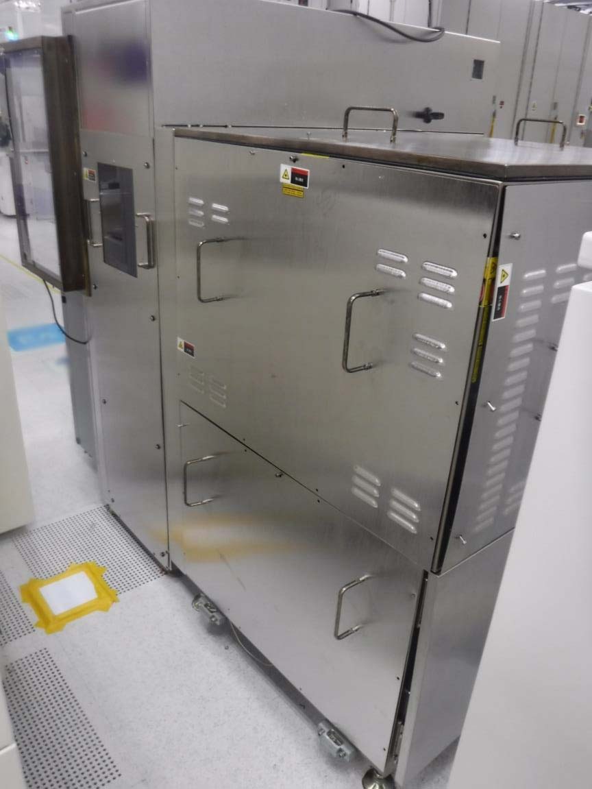
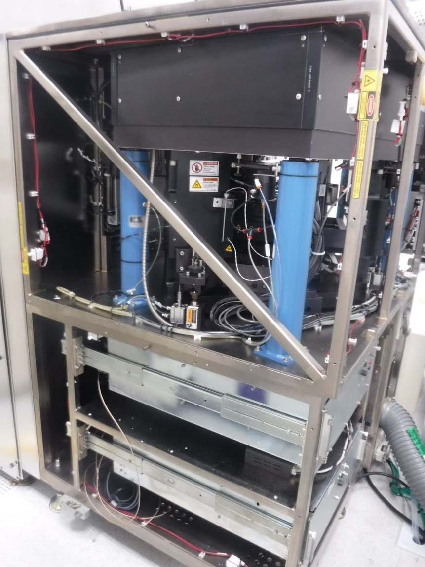
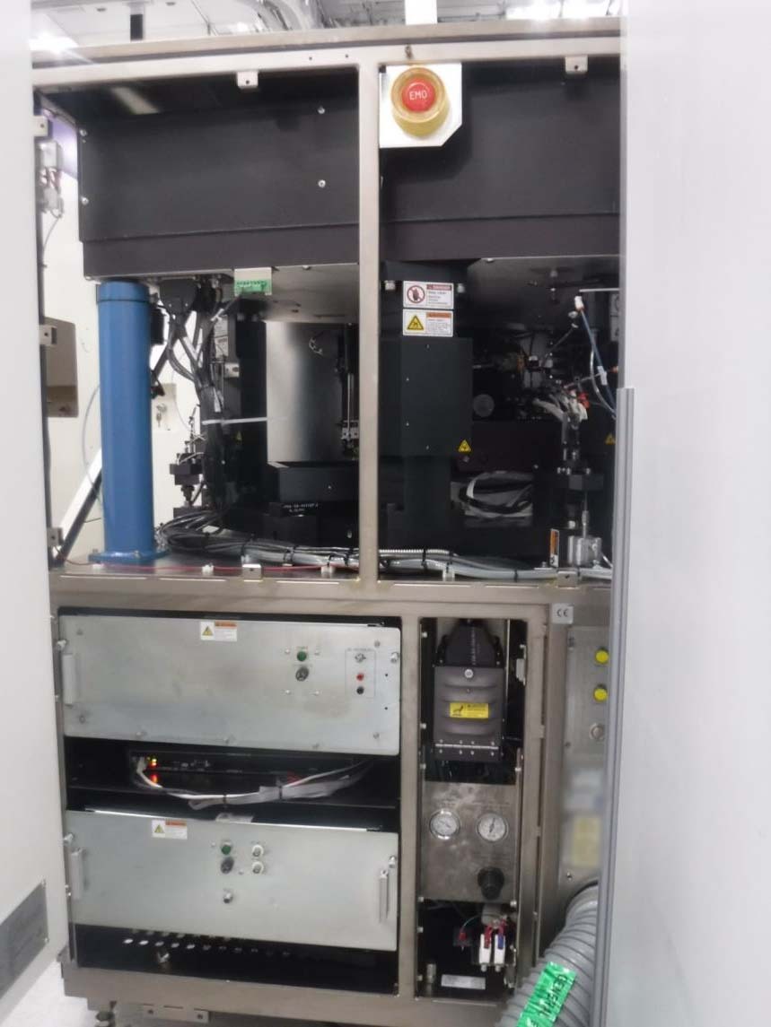
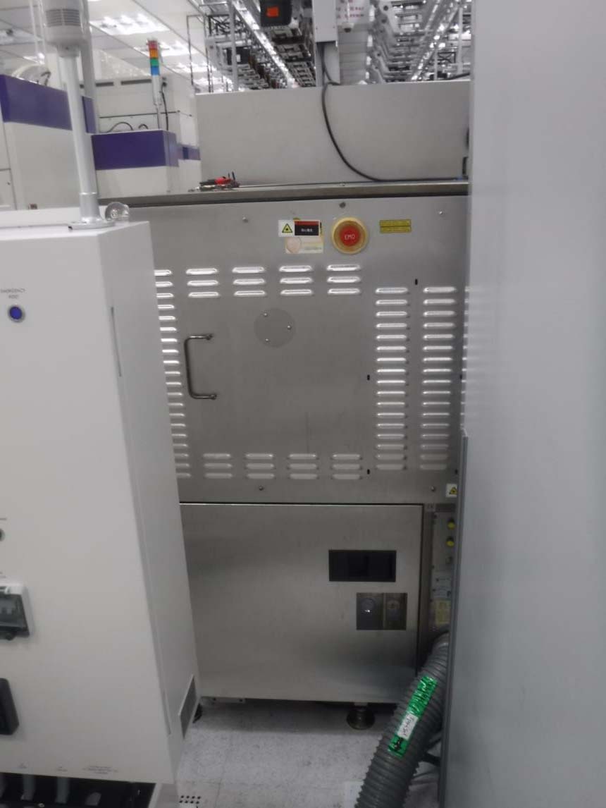
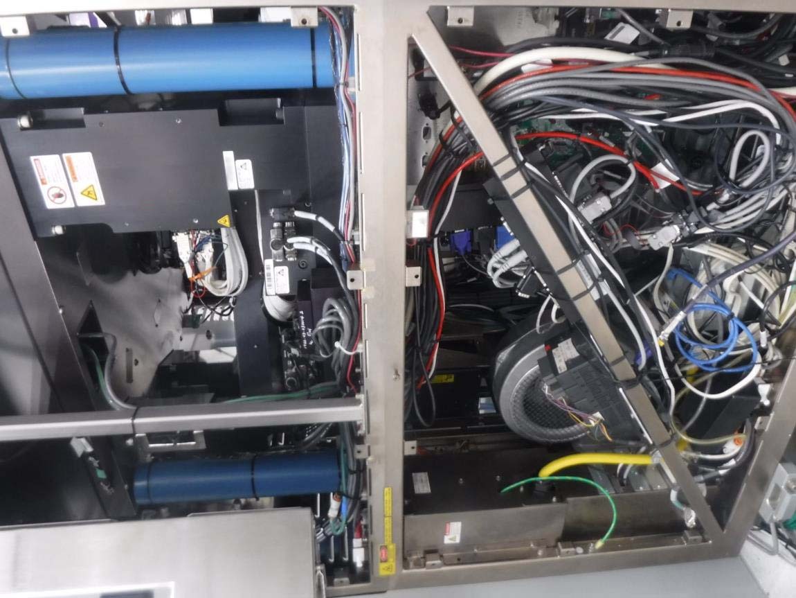
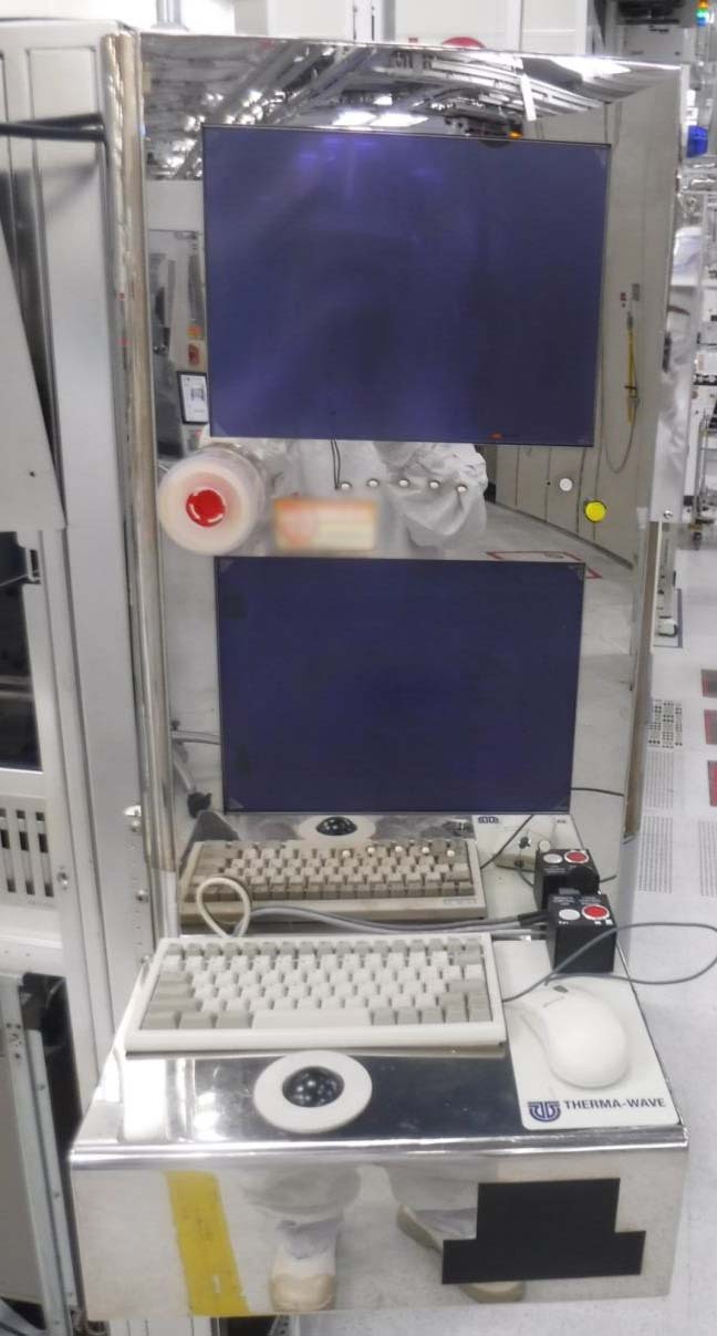
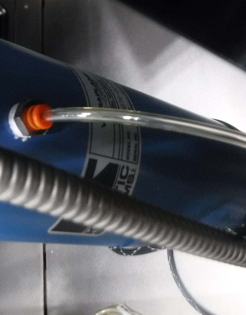
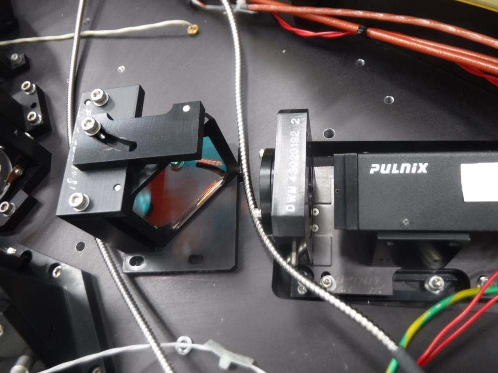
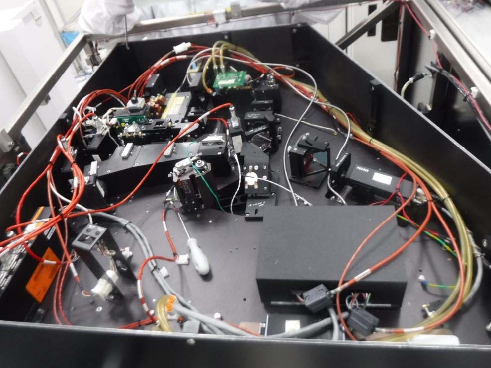
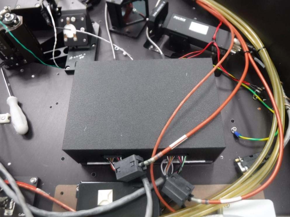
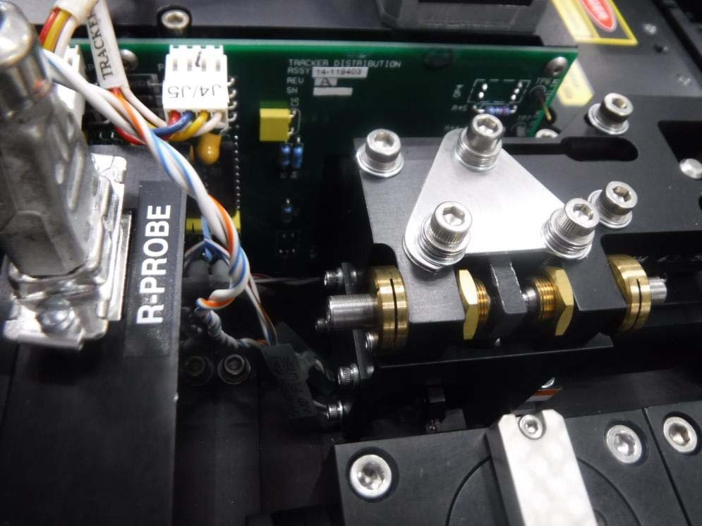
ID: 293759748
Vintage: 2006
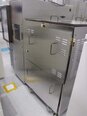
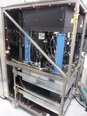
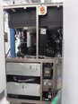
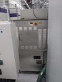
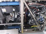
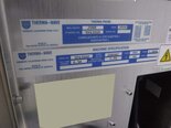
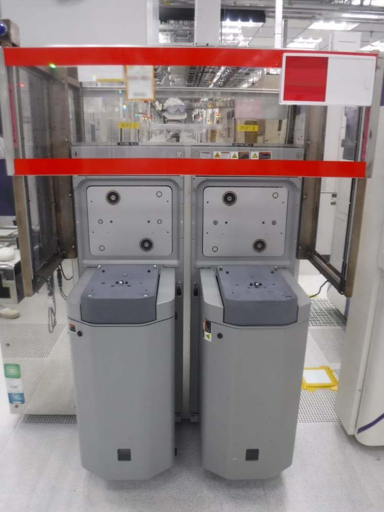
Metrology system
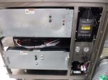
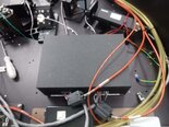
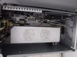
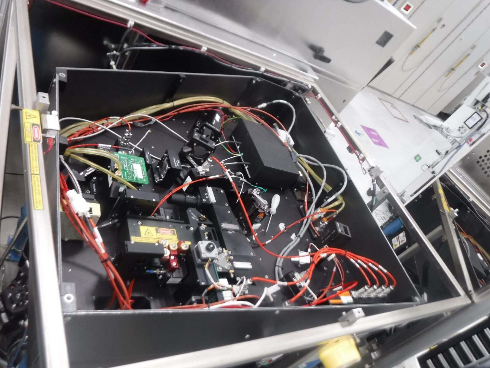
Lamp housing
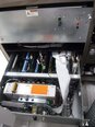
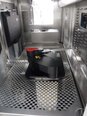
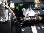
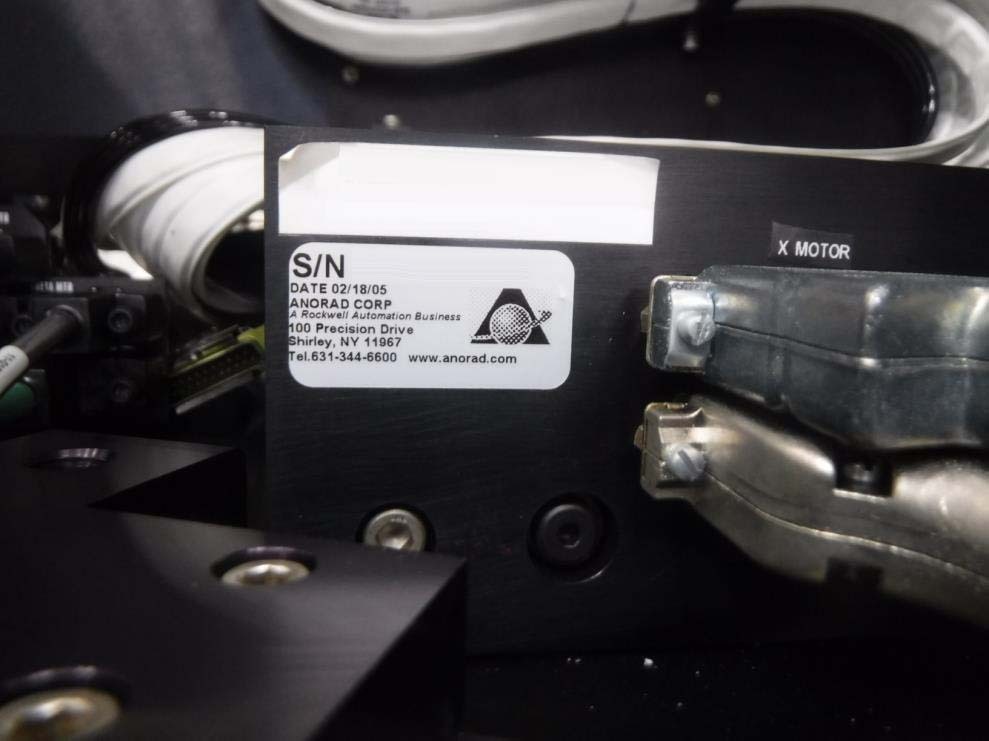
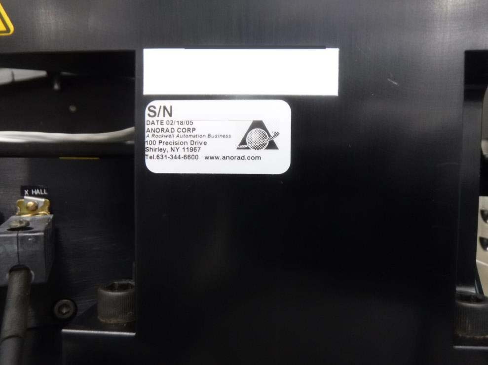
ANORAD Stage assy
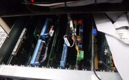
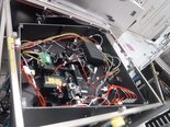
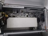
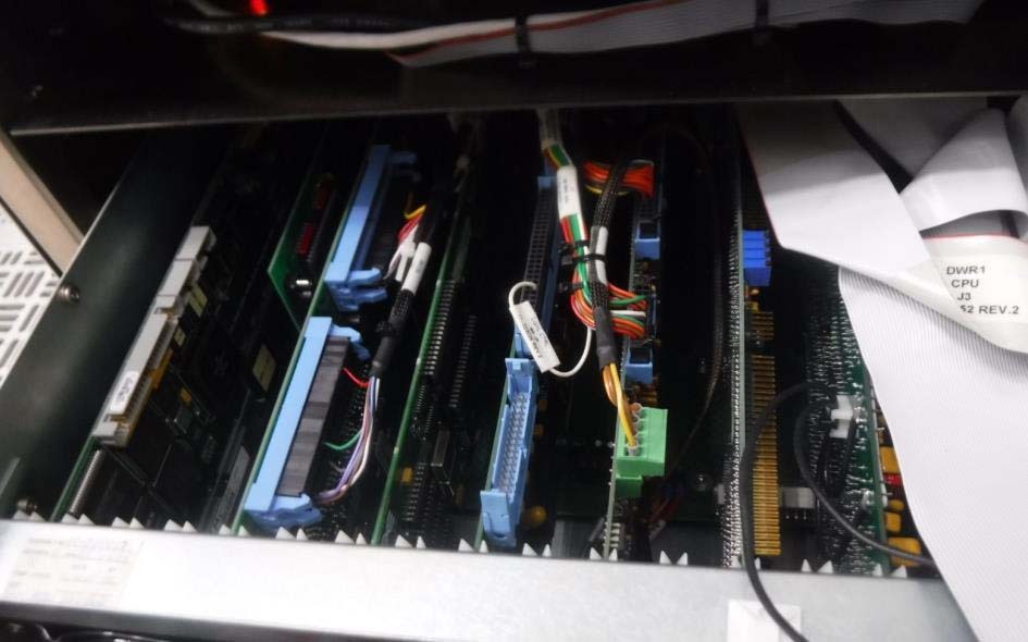
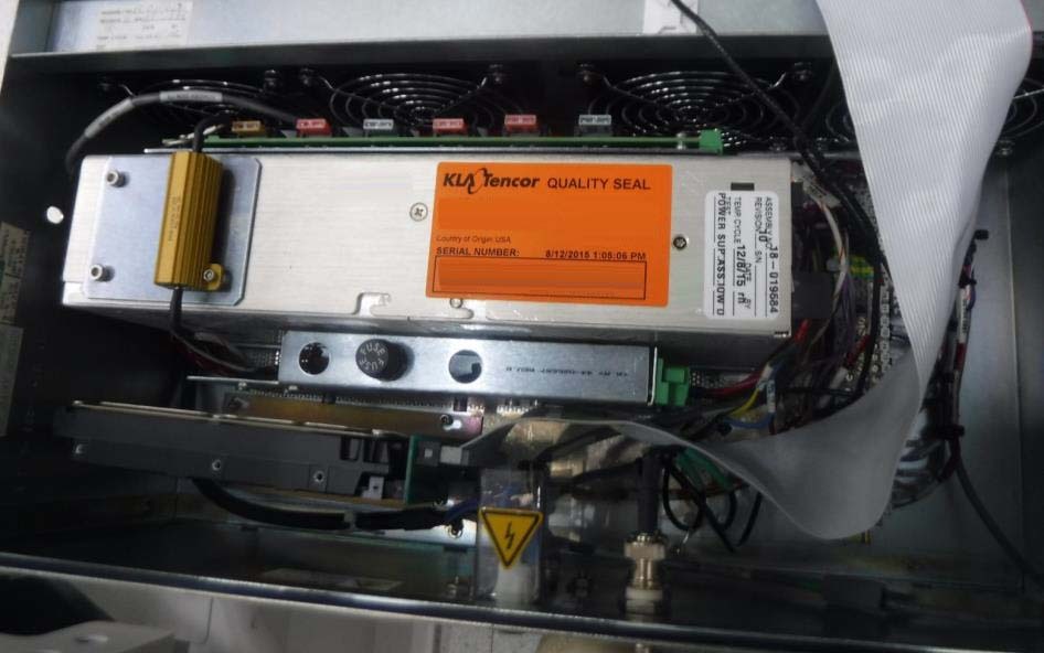
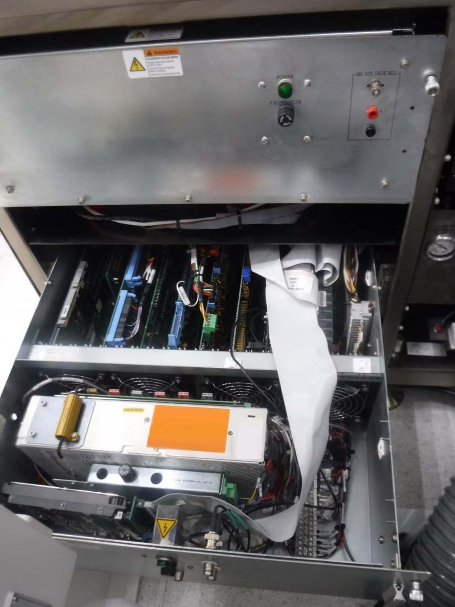
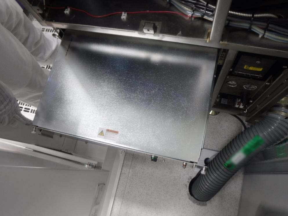
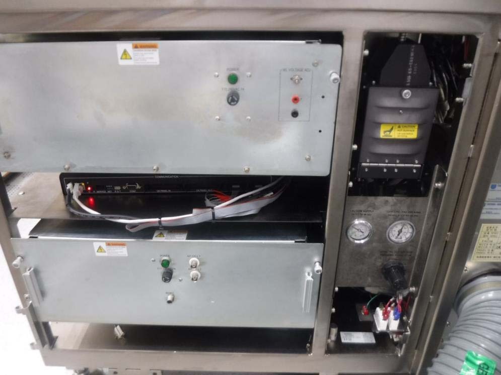
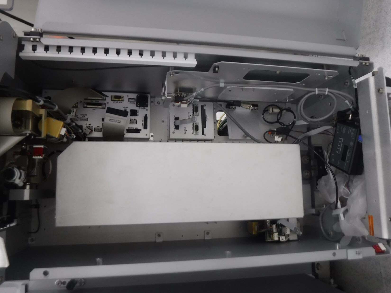
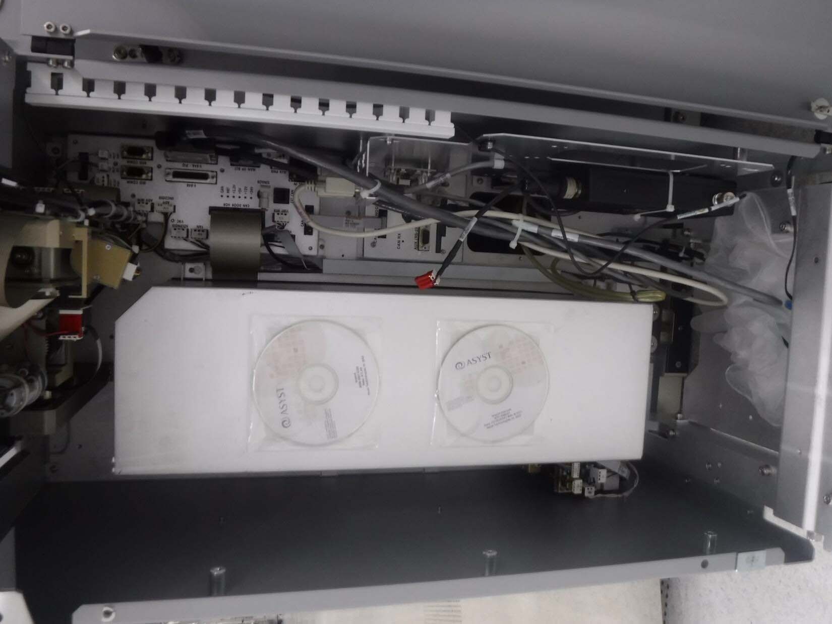
Upper drawer
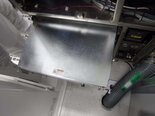
Lower drawer
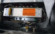
Laser
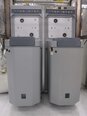
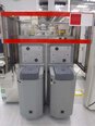
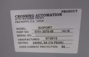
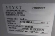
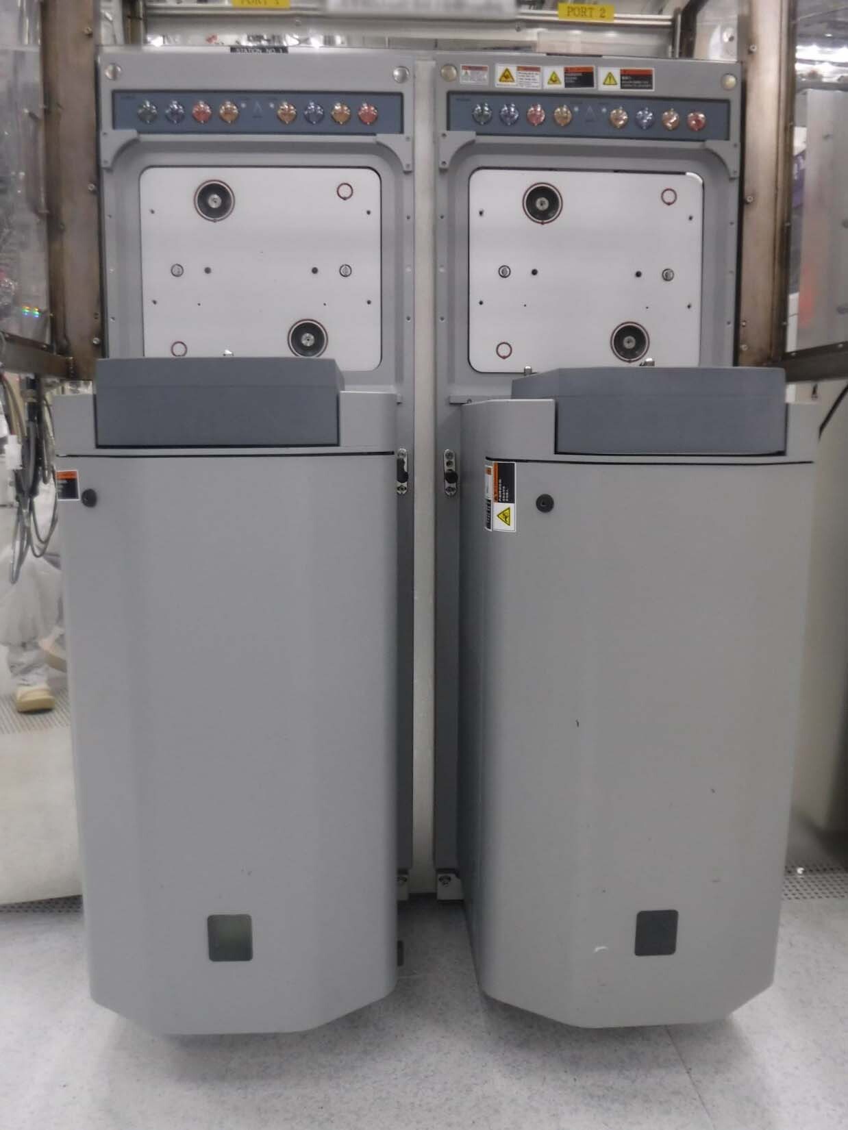
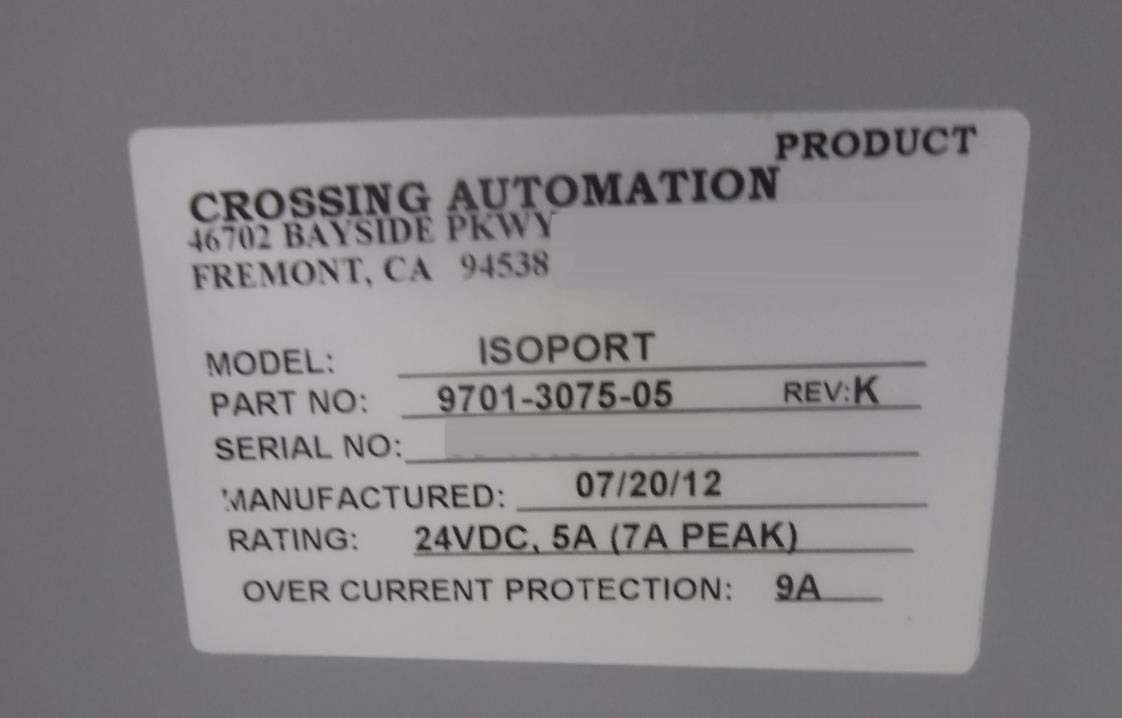
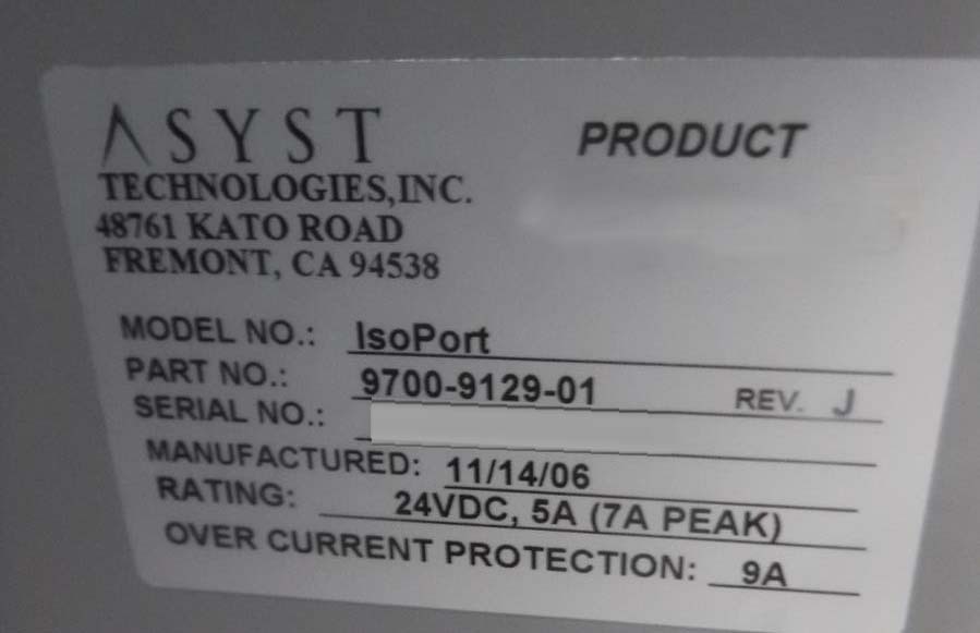
(2) ASYST ISOPORT Load ports
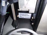
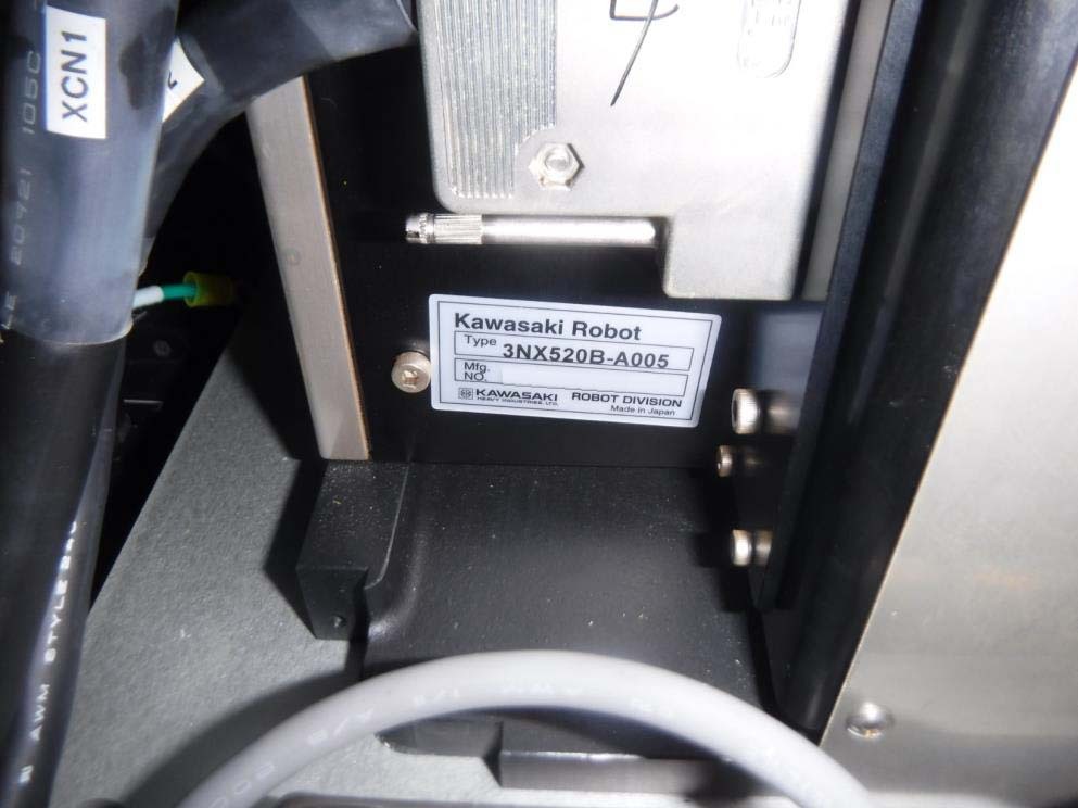
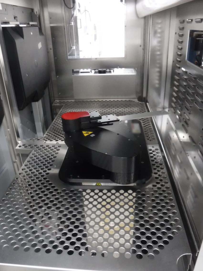
KAWASAKI 3NX520B-A005 Robot
Aligner
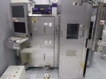
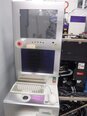
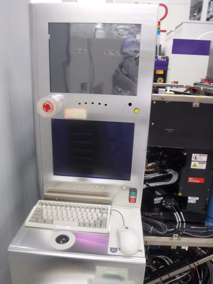
Front UI
Rear UI
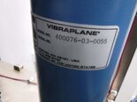
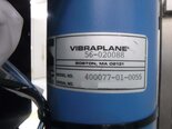
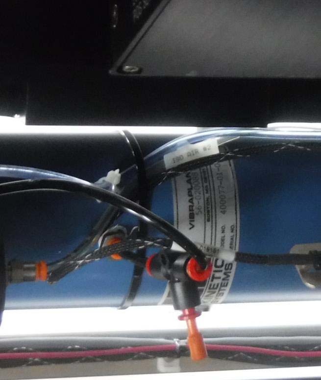
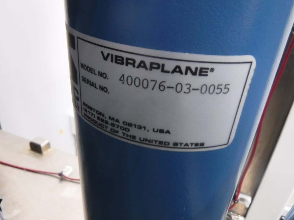
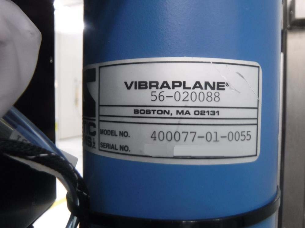
(4) KINETIC SYSTEMS Vibraplane
Part number:
40077-01-0055
40076-03-0055
40076-02-0055
40077-01-0055
PC
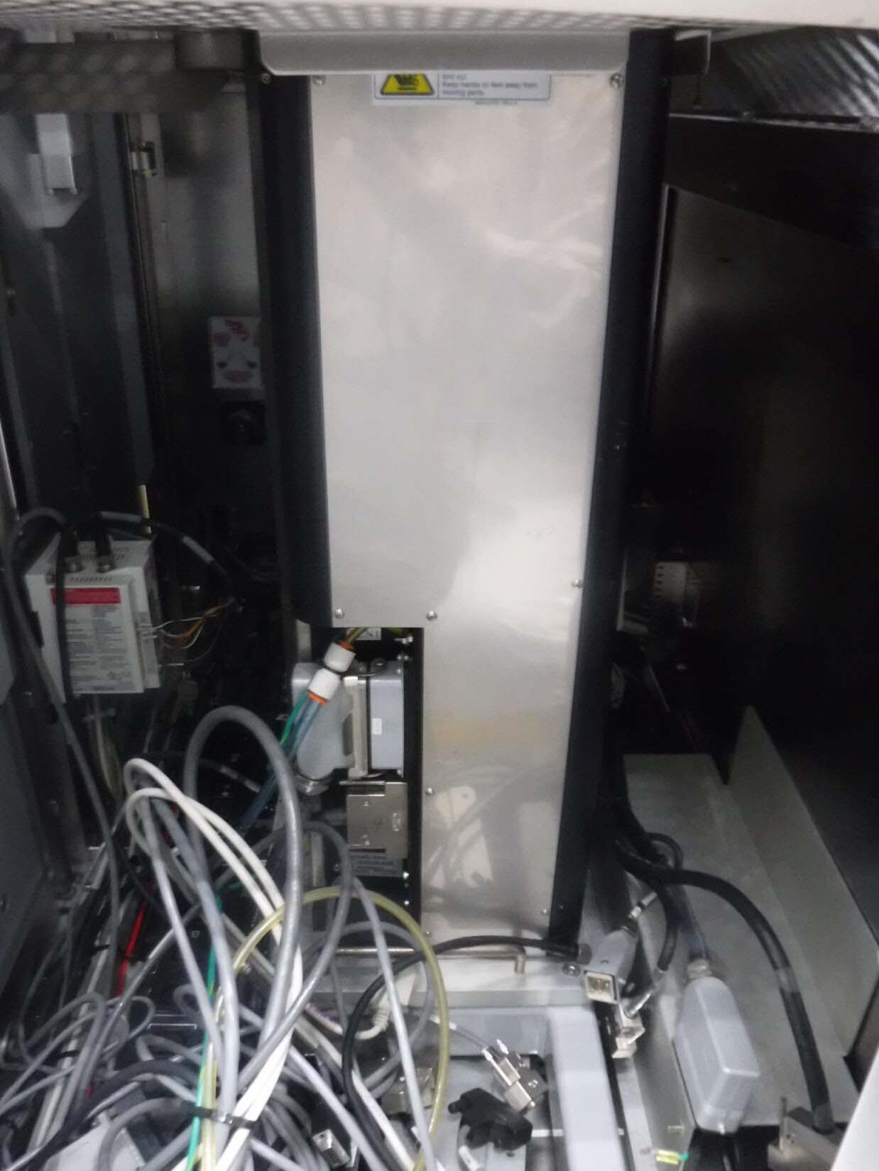
Robot controller missing
2006 vintage.
KLA / TENCOR / THERMA-WAVE TP 630XP is an advanced wafer testing and metrology equipment designed to provide comprehensive analysis and characterization of semiconductor wafers. As a critical component of the semiconductor manufacturing process, this system is utilized for quality control, process optimization, and yield enhancement. By offering a suite of innovative features and capabilities, KLA TP 630XP enables semiconductor manufacturers to meet the demanding requirements of modern integrated circuit fabrication. One of the key features of TENCOR TP630XP is its non-contact, non-destructive measurement capabilities. Utilizing advanced optical technologies, the unit can accurately measure critical parameters such as film thickness, composition, and dopant concentration without the need for physical contact with the wafer surface. This non-invasive measurement approach eliminates the risk of damage to the fragile semiconductor materials, ensuring the integrity of the test data and the continued functionality of the wafers. TENCOR TP 630XP is equipped with a range of measurement modes and techniques to address various wafer testing requirements. The machine can perform reflectance measurements, spectroscopic ellipsometry, and spectral reflectance analysis to characterize the optical properties of thin films and semiconductor layers. These measurements provide valuable insights into film thickness variations, refractive index changes, and composition profiles across the wafer surface. In addition to optical measurements, KLA / TENCOR / THERMA-WAVE TP630XP offers advanced electrical characterization capabilities for analyzing the electronic properties of semiconductor devices. By integrating techniques such as capacitance-voltage (CV) measurements, spreading resistance profiling (SRP), and sheet resistance mapping, the tool can assess device performance, detect defects, and optimize process parameters to improve device yield and reliability. Furthermore, KLA TP630XP features high-resolution imaging capabilities for visual inspection and defect analysis. The asset is equipped with state-of-the-art microscopy modules that enable users to capture detailed images of wafer surfaces, identify defects, and perform root cause analysis to troubleshoot process issues and enhance yield. To streamline the data analysis and reporting process, TP 630XP integrates powerful software tools for data visualization, interpretation, and correlation. The model can generate comprehensive reports with detailed measurement results, statistical analysis, and trend monitoring to support decision-making and process improvement initiatives within the semiconductor manufacturing environment. Overall, THERMA-WAVE TP630XP represents a cutting-edge solution for wafer testing and metrology in the semiconductor industry. With its advanced measurement techniques, non-destructive approach, and comprehensive analysis capabilities, the equipment empowers semiconductor manufacturers to achieve higher levels of quality, performance, and efficiency in their production processes. By leveraging the capabilities of THERMA-WAVE TP 630XP, semiconductor companies can drive innovation, reduce time-to-market, and enhance their competitive edge in the fast-paced semiconductor market.
There are no reviews yet