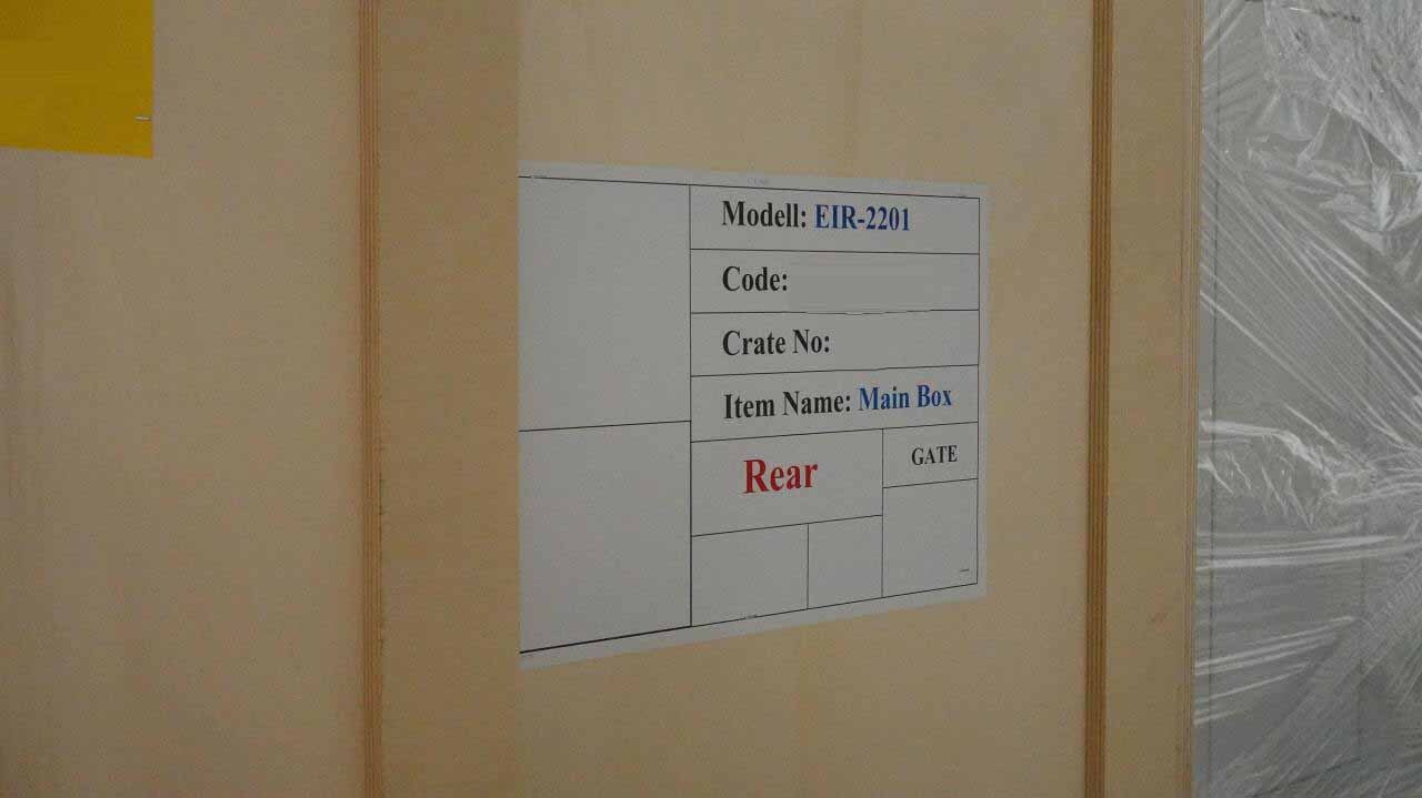
Used SEMILAB EIR-2201 #293802484 for sale
URL successfully copied!



Tap to zoom
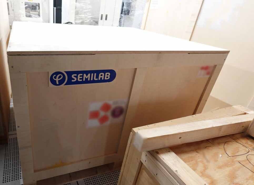

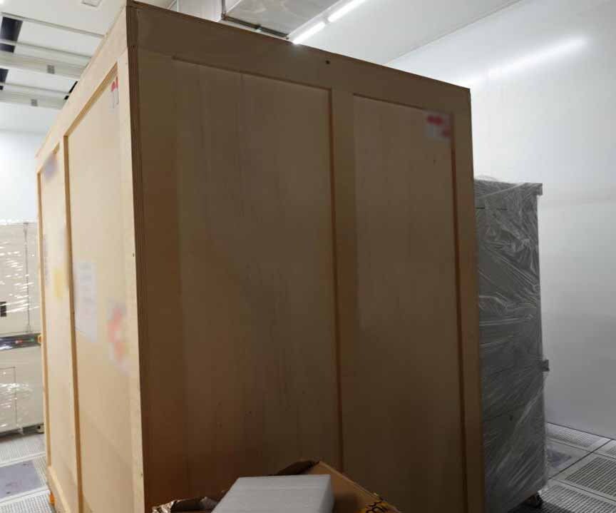

ID: 293802484
Wafer Size: 6"
FT-IR System, 6"
(2) Open cassette load ports
X-Y Mapping stage: 200 mm
3-Color signal tower
HMI
Utility specification:
Connection type: Swagelok female
Utility type / Connection size / Pressure / Flow
Nitrogen N2 / 3/8" / 550-830 KPa / 3-5 SLM
Nitrogen exhaust / 1/2" / - / 4 SLM
Vacuum / 3/8" / -65 KPa / 15 SLM
Clean Dry Air (CDA) / 3/8" / - / 10 SLM
Environment and vibration specification:
Ambient temperature: 20° to 25° C
Humidity: Between 20% and 50%
Vibration sensitivity: VC-B
Maximum power consumption: 1.5 kW
Full load current: 17.5 A / 8.3 A
Apparent power: 575 VA
Power supply: 110-230 VAC, Single phase, 20 A, 3 Wires, 50/60 Hz.
SEMILAB EIR-2201 is a cutting-edge wafer testing and metrology equipment that offers high precision and accuracy in measuring various parameters of semiconductor wafers. This advanced tool incorporates state-of-the-art technology to provide semiconductor manufacturers with the ability to analyze and characterize wafers quickly and efficiently, ensuring the production of high-quality semiconductor devices. At the core of EIR-2201 is its advanced optical and electrical measurement capabilities. The system utilizes a combination of techniques such as ellipsometry, reflectometry, and spectroscopic imaging to capture detailed information about the physical and chemical properties of the wafer surfaces. These measurements are critical for understanding the structural characteristics, material composition, and performance of the semiconductor devices being manufactured. One of the key features of SEMILAB EIR-2201 is its ability to perform non-destructive measurements on wafers of various sizes and materials. The unit is designed to handle both standard and advanced semiconductor materials, including silicon, compound semiconductors, and thin films. This versatility enables semiconductor manufacturers to analyze a wide range of wafer types and structures without the need for multiple testing tools. In terms of metrology capabilities, EIR-2201 offers high spatial resolution and sensitivity, allowing for detailed analysis of even the smallest features on the wafer surface. The machine can map out thickness variations, refractive indices, and other parameters with micron-level precision, providing valuable insights into the uniformity and quality of the semiconductor materials. Moreover, SEMILAB EIR-2201 is equipped with advanced data analysis and visualization tools that enable users to process and interpret the measurement data effectively. The tool can generate detailed reports, graphs, and images that help semiconductor engineers and researchers understand the characteristics of the wafers and make informed decisions about process optimization and device design. Another notable feature of EIR-2201 is its user-friendly interface and automation capabilities. The asset is designed to streamline the wafer testing process, allowing users to set up experiments, run measurements, and analyze results with ease. Its intuitive software interface provides flexibility in customizing measurement protocols and parameters to suit specific testing requirements. Additionally, SEMILAB EIR-2201 is equipped with advanced data management and connectivity options, enabling seamless integration with semiconductor manufacturing workflows. The model can communicate with other equipment, databases, and software tools to streamline data transfer and analysis, ensuring efficient collaboration and decision-making within the production environment. In summary, EIR-2201 is a sophisticated wafer testing and metrology equipment that combines advanced optical and electrical measurement techniques with high precision and automation capabilities. Its versatility, accuracy, and user-friendly interface make it an essential tool for semiconductor manufacturers looking to optimize the quality and performance of their devices.
There are no reviews yet