Used SEMILAB SSM2000 #293665614 for sale
URL successfully copied!



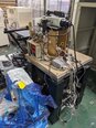
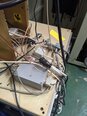
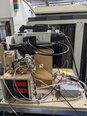
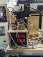

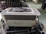
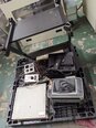
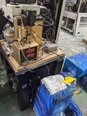

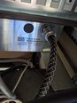
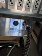
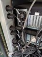
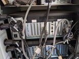

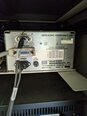
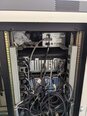
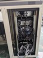
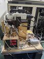
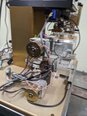
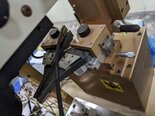
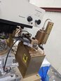
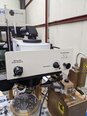
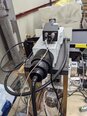
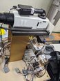
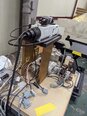
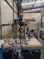
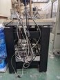
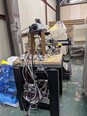
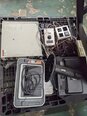
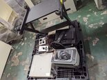
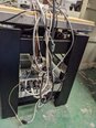
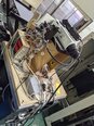

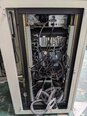
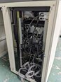
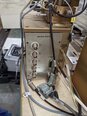
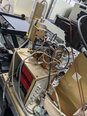
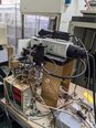
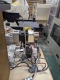
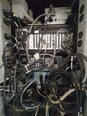
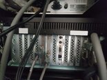
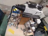
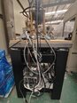
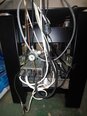
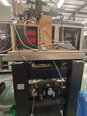
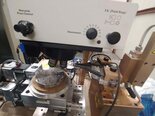
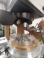
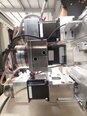
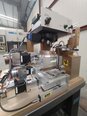
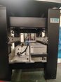





Tap to zoom
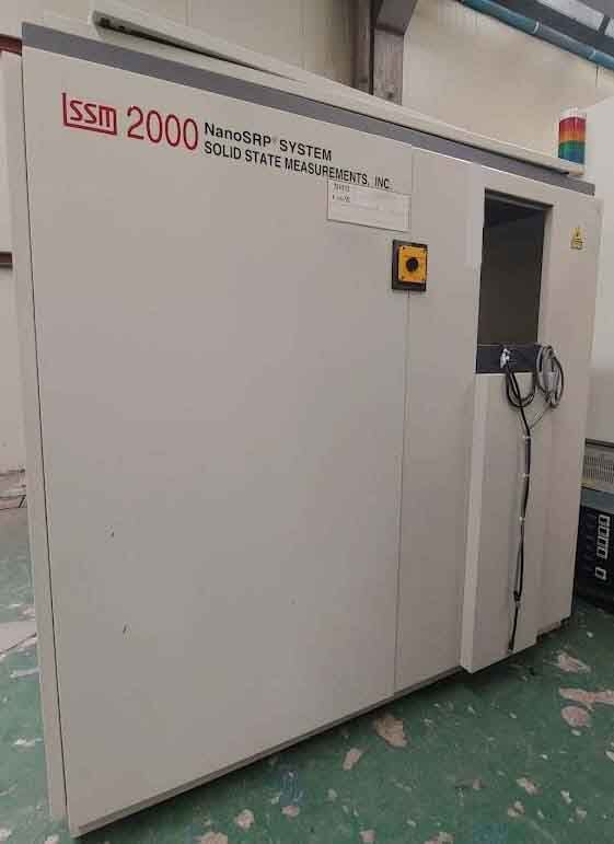

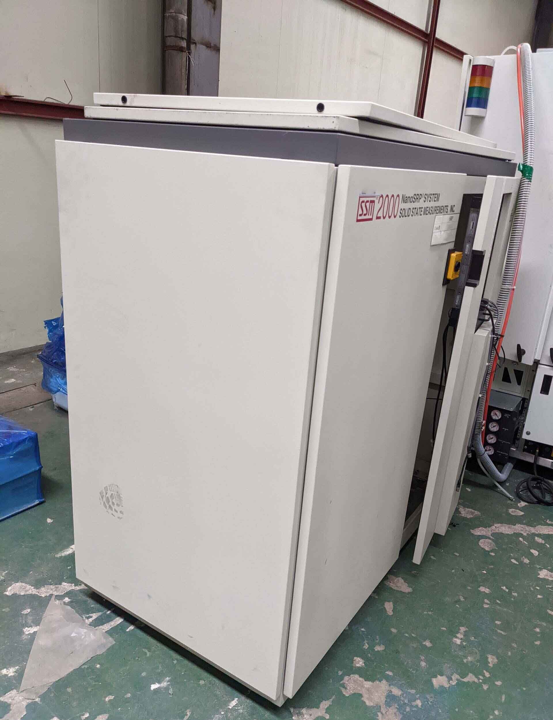
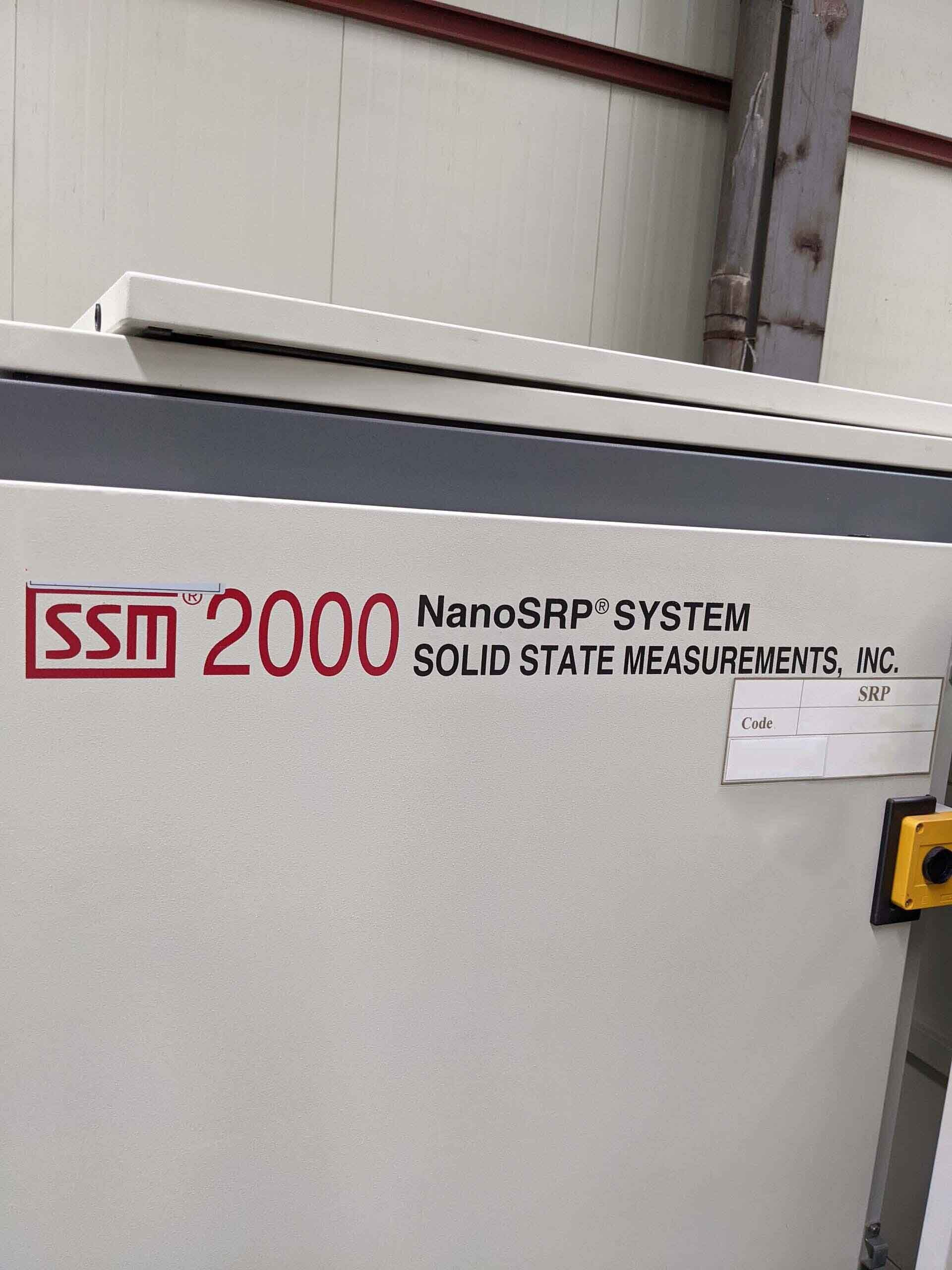
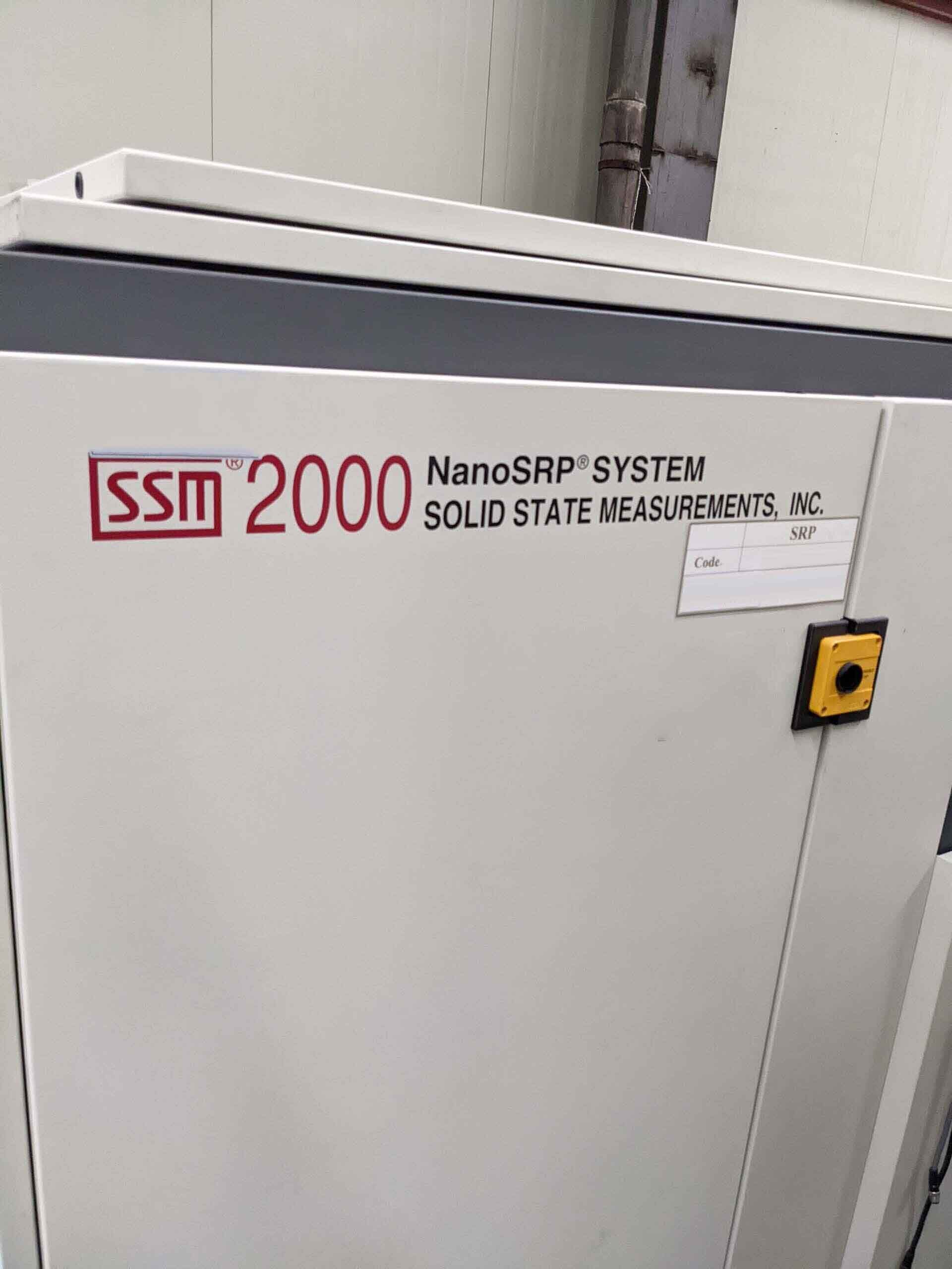
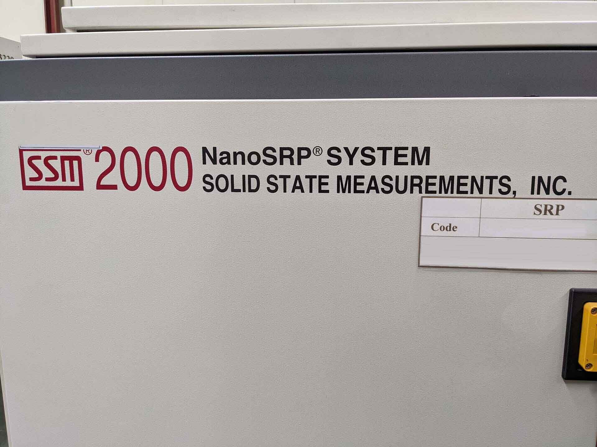
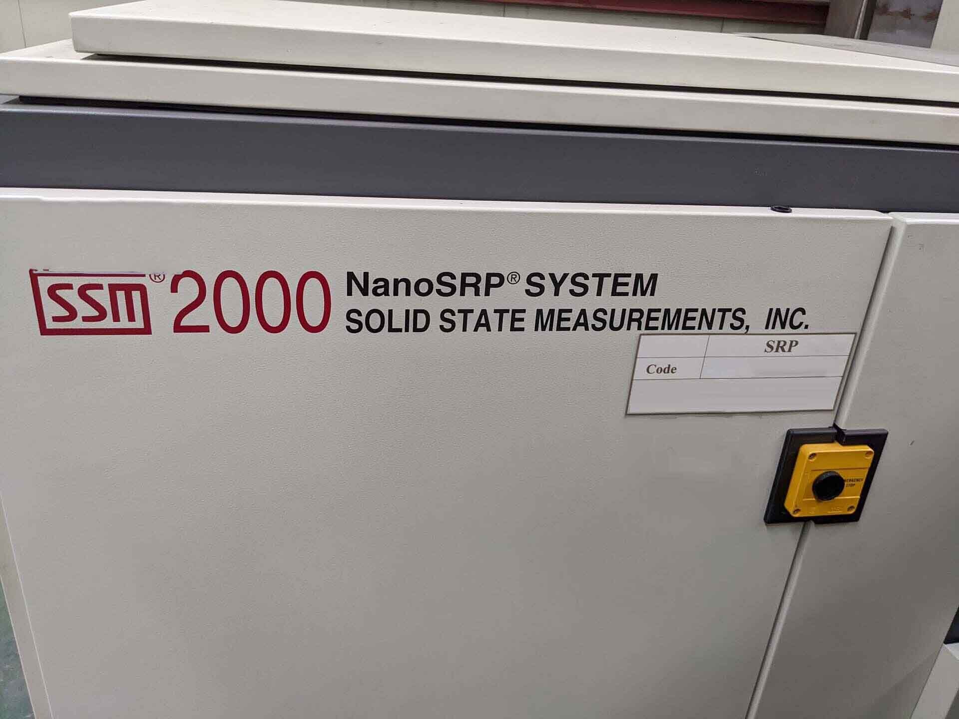
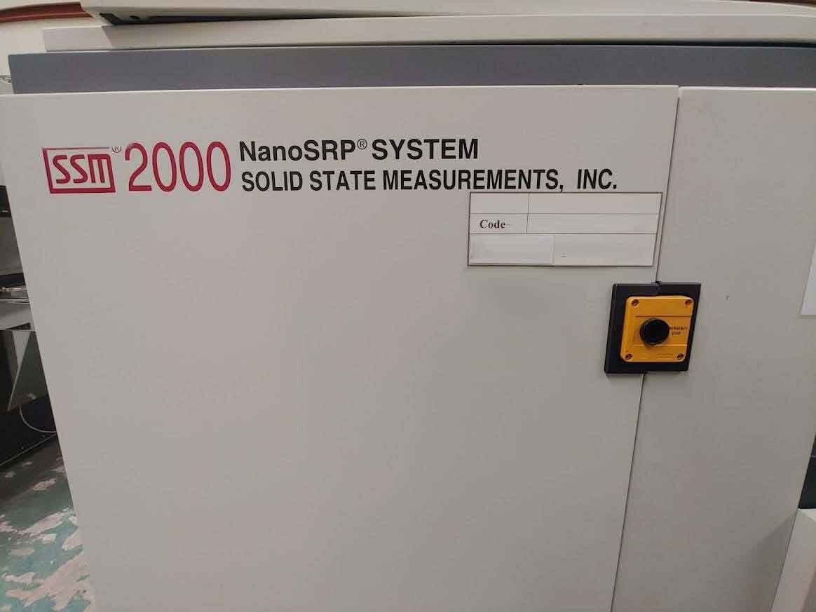
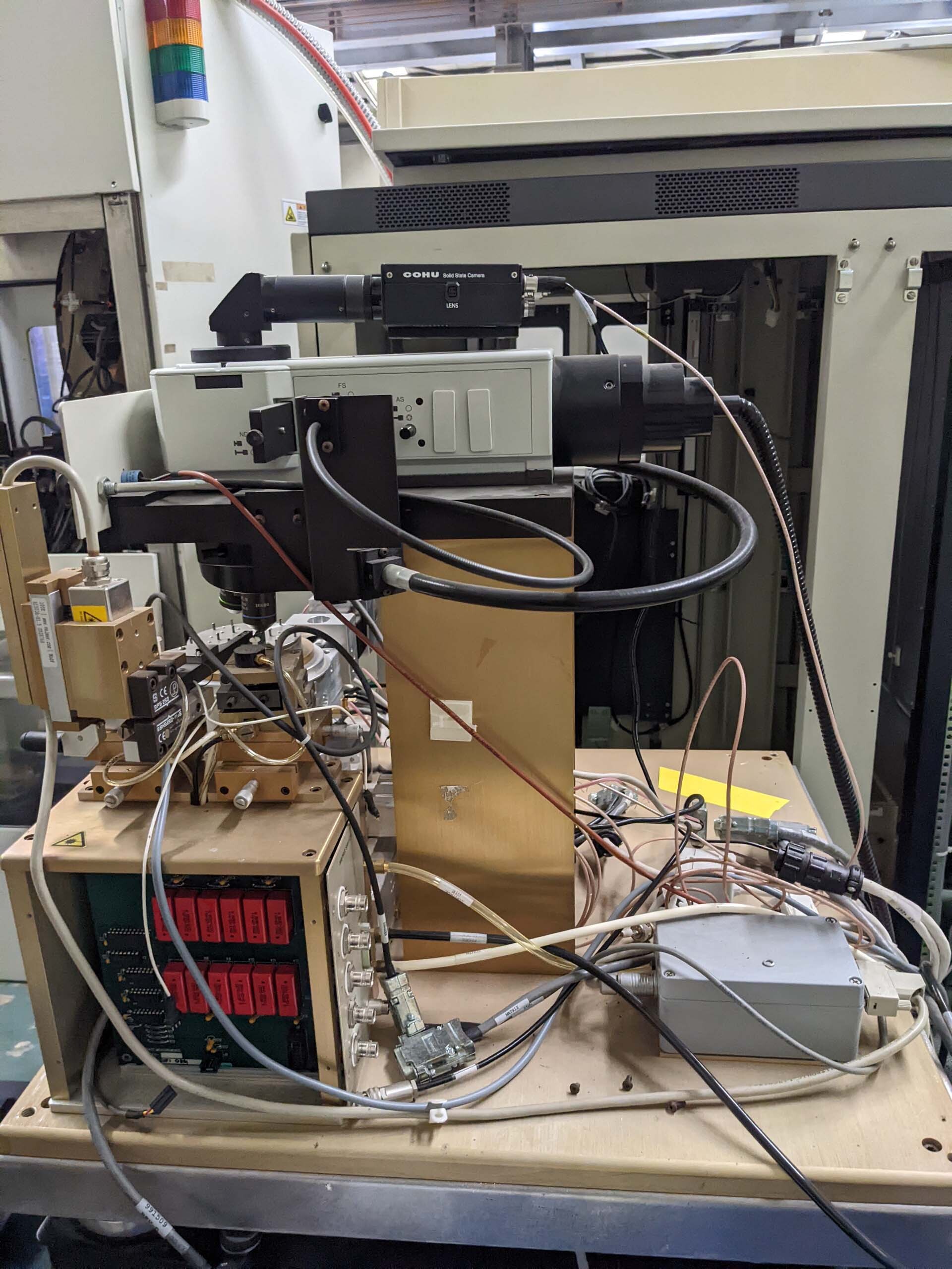
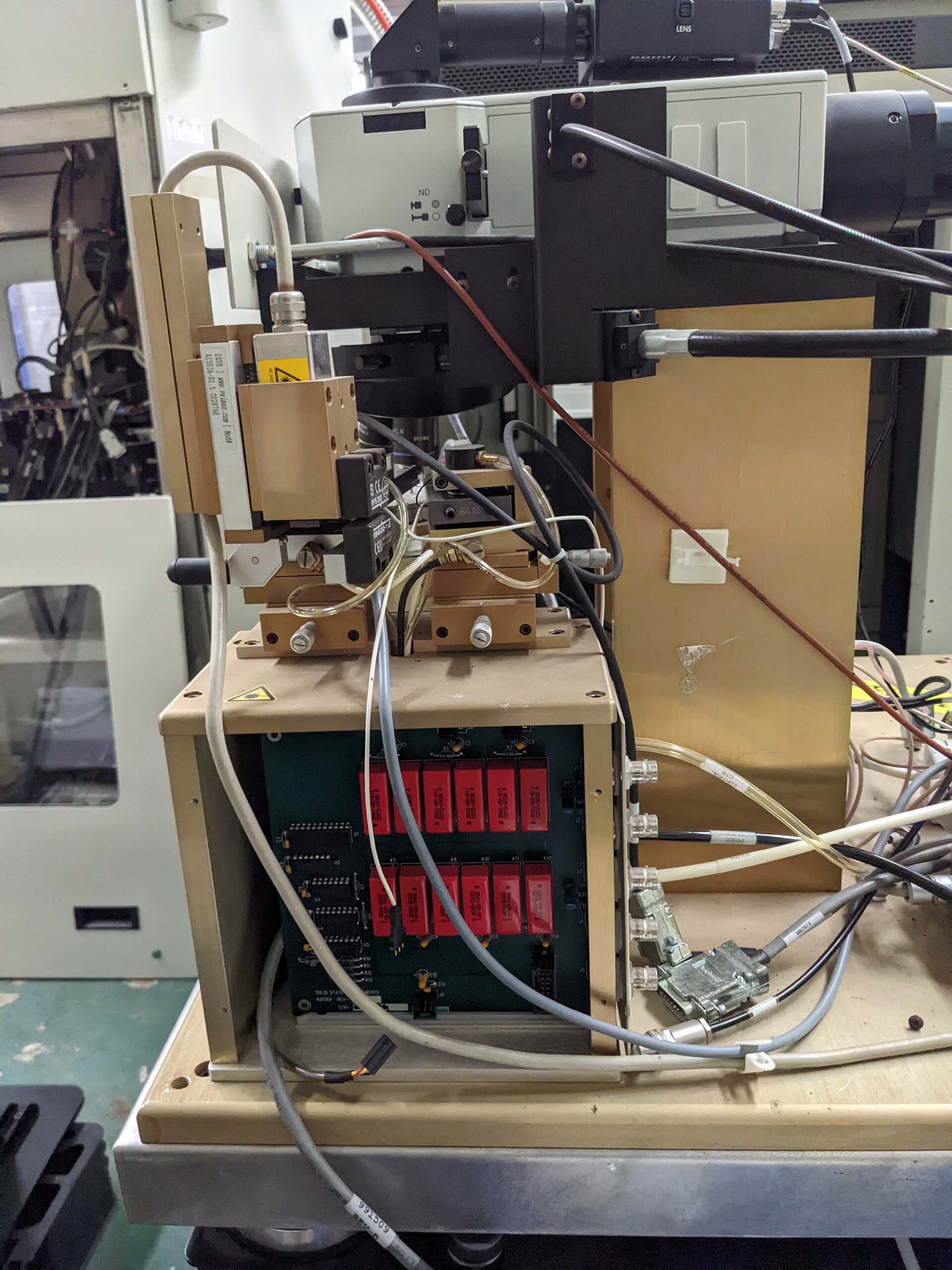
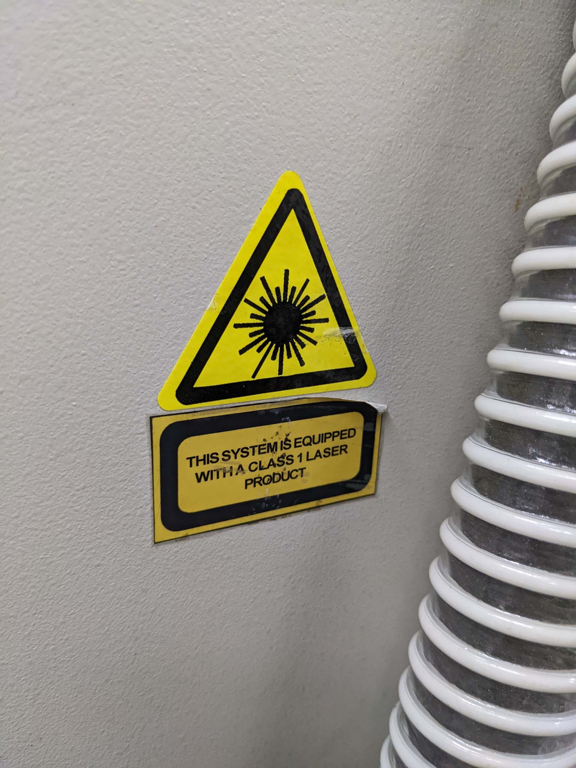
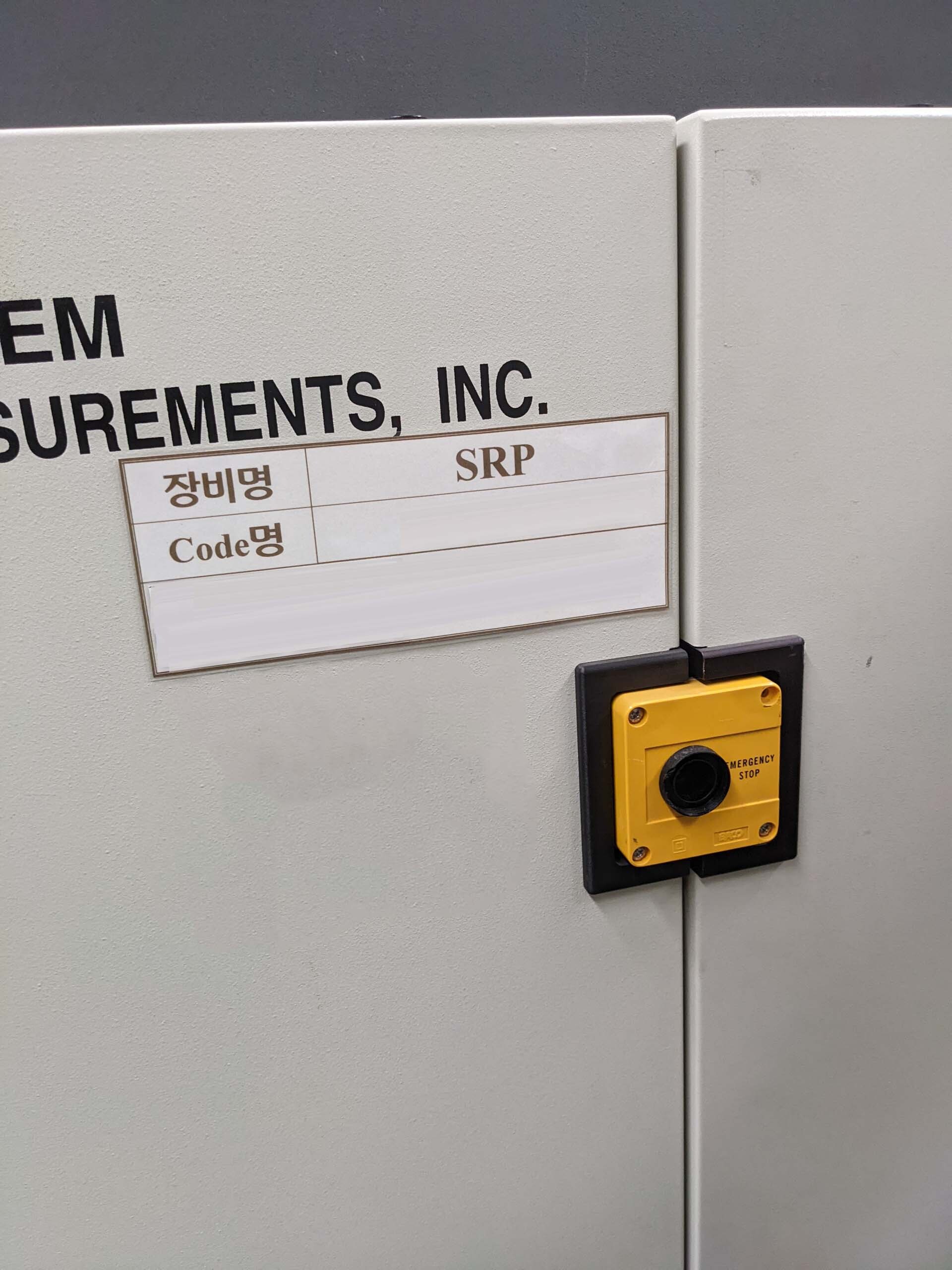
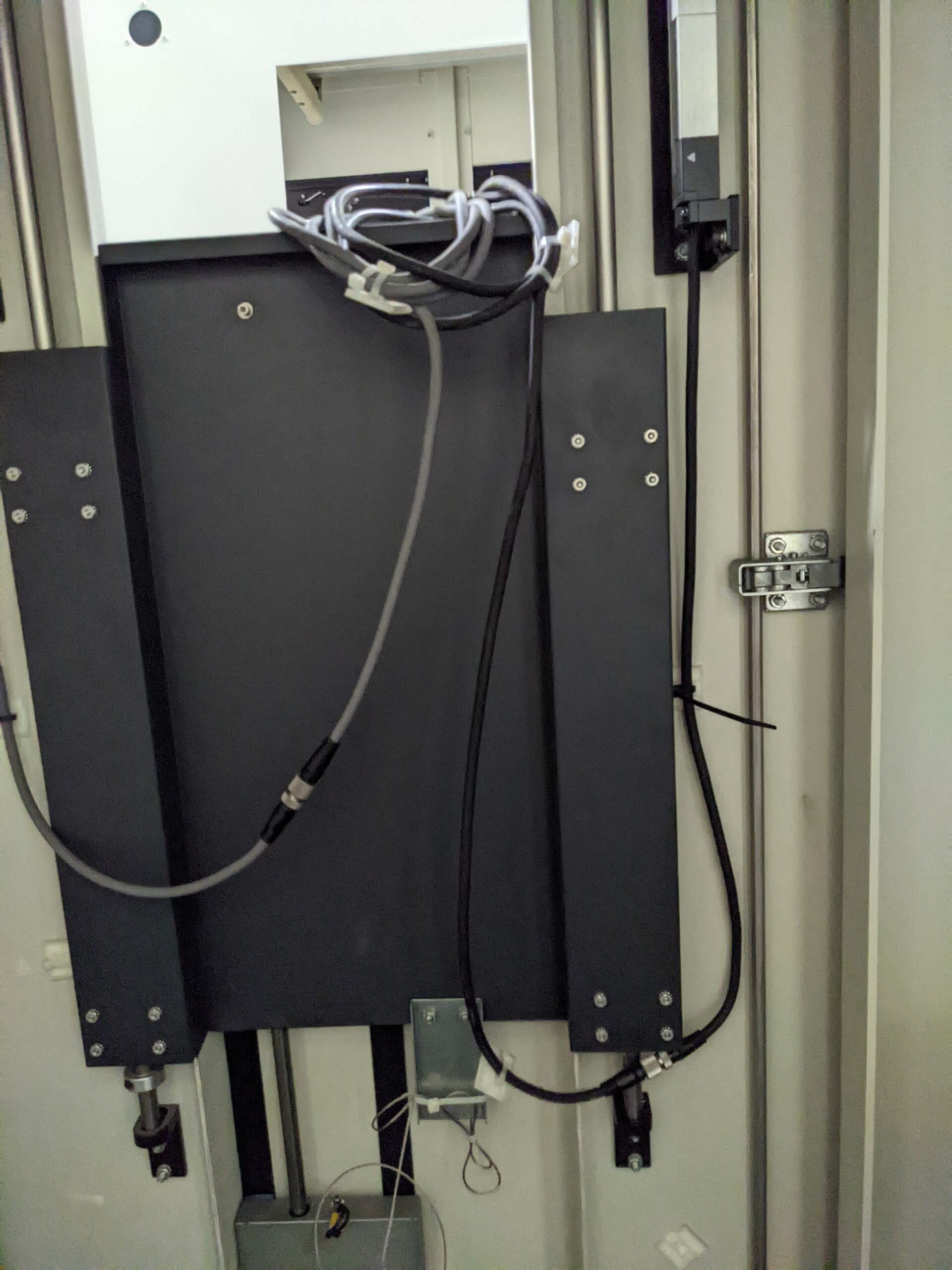
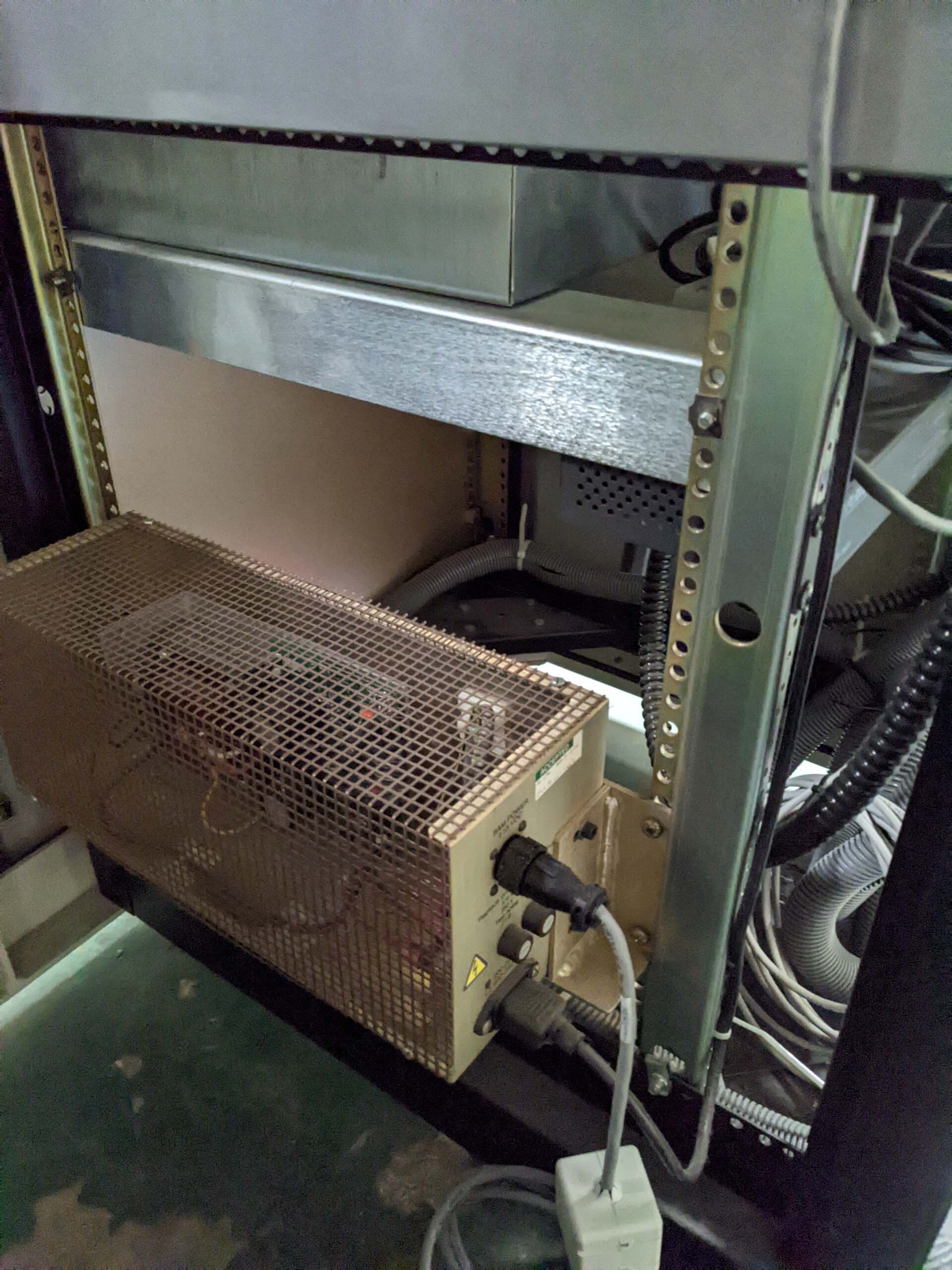
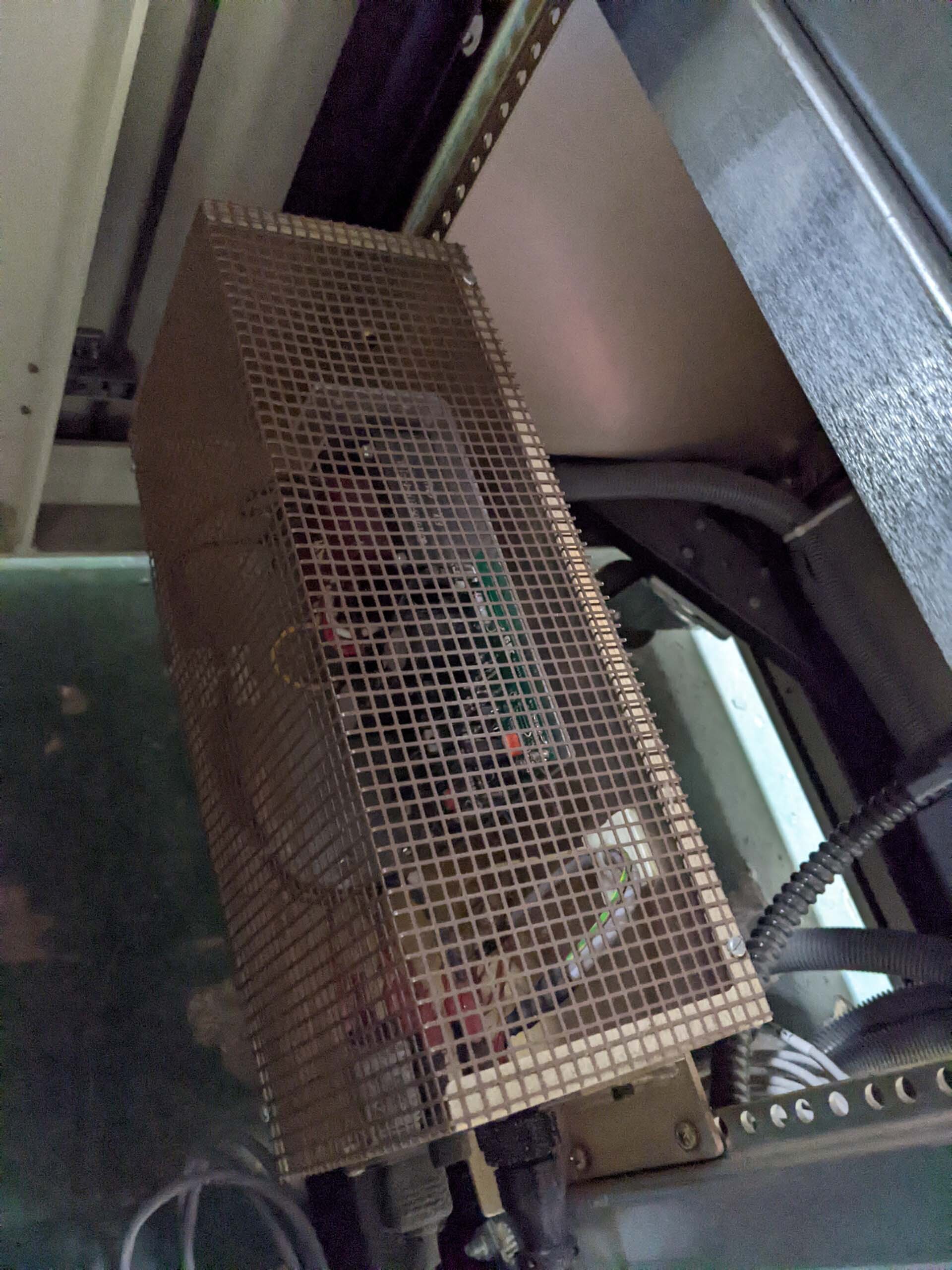
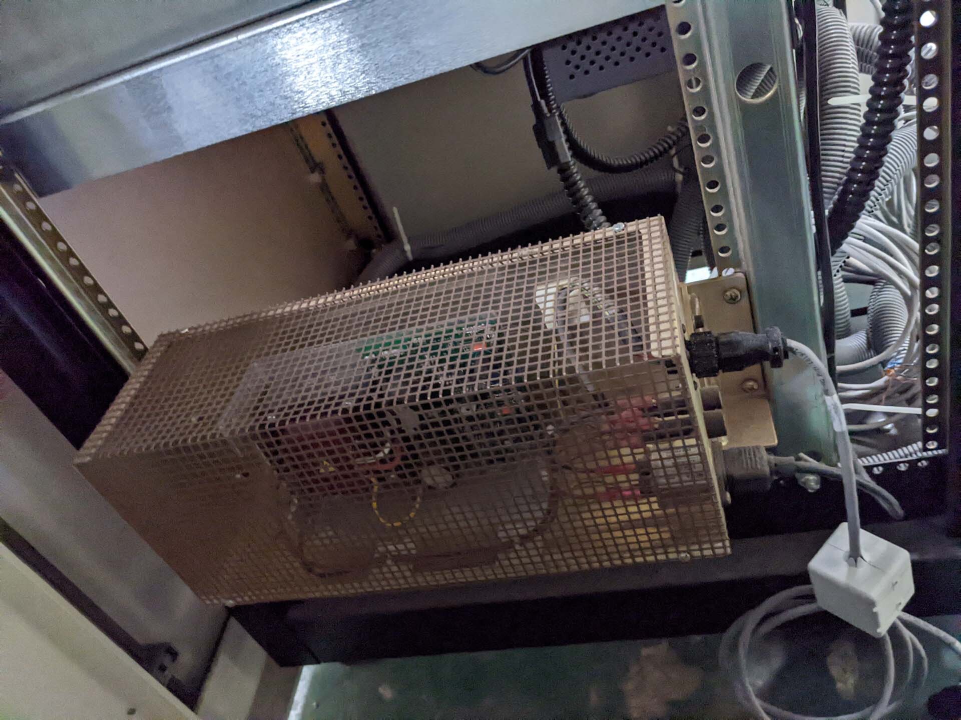
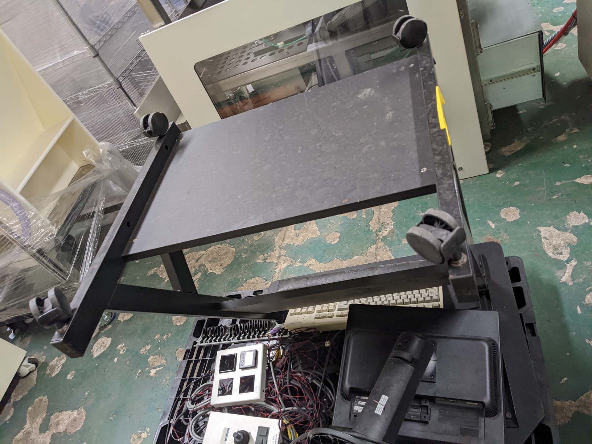
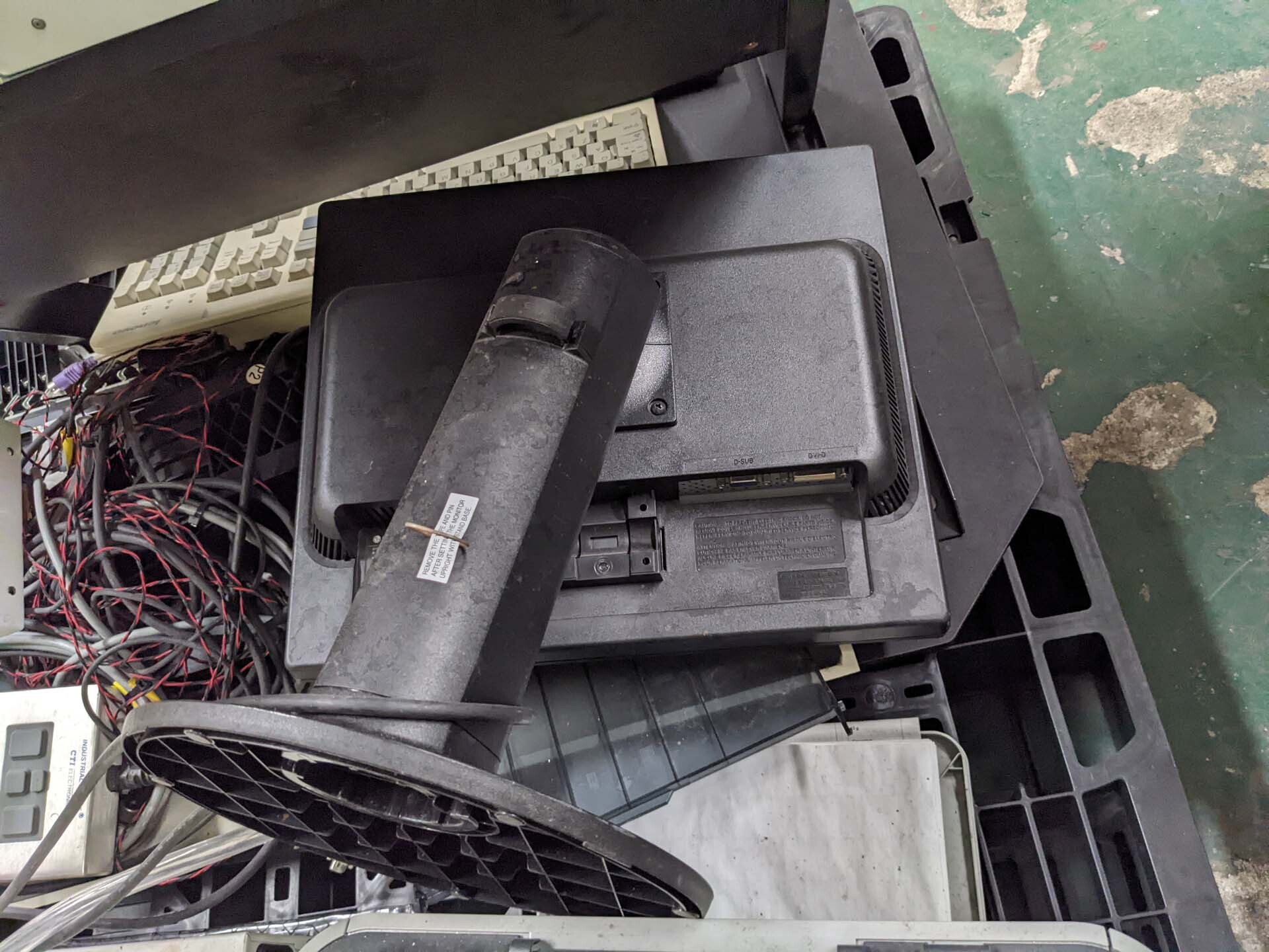
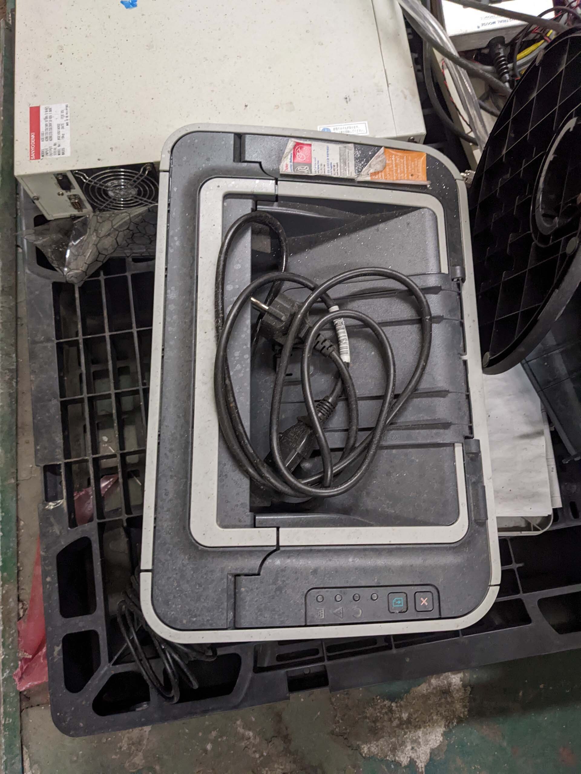
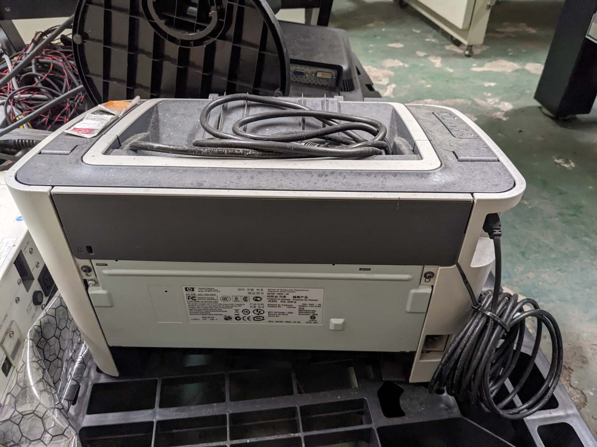

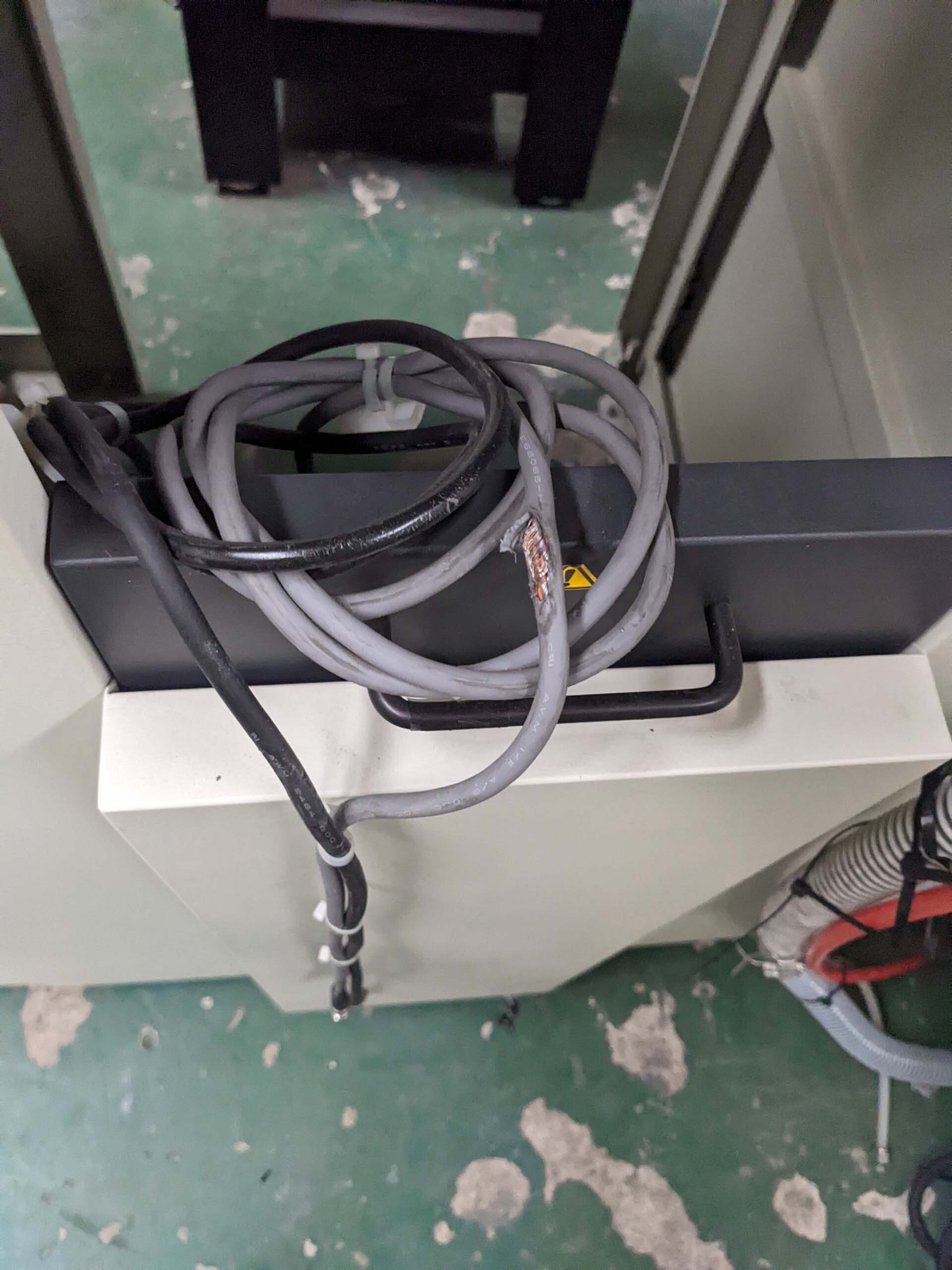
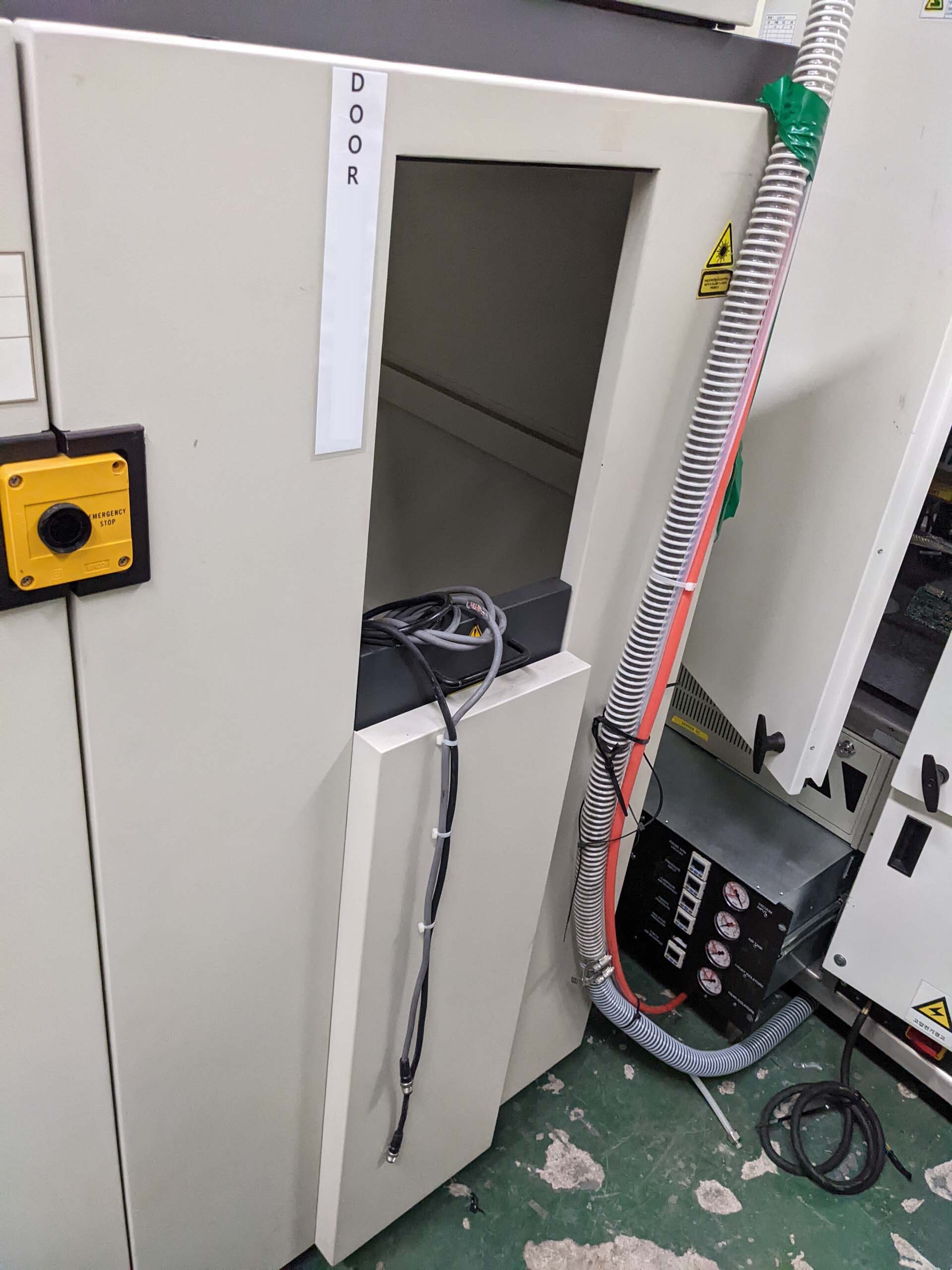
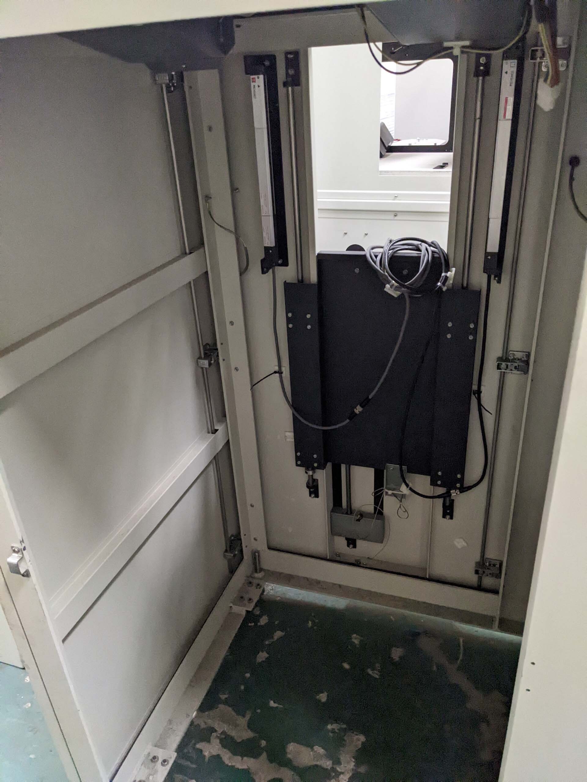
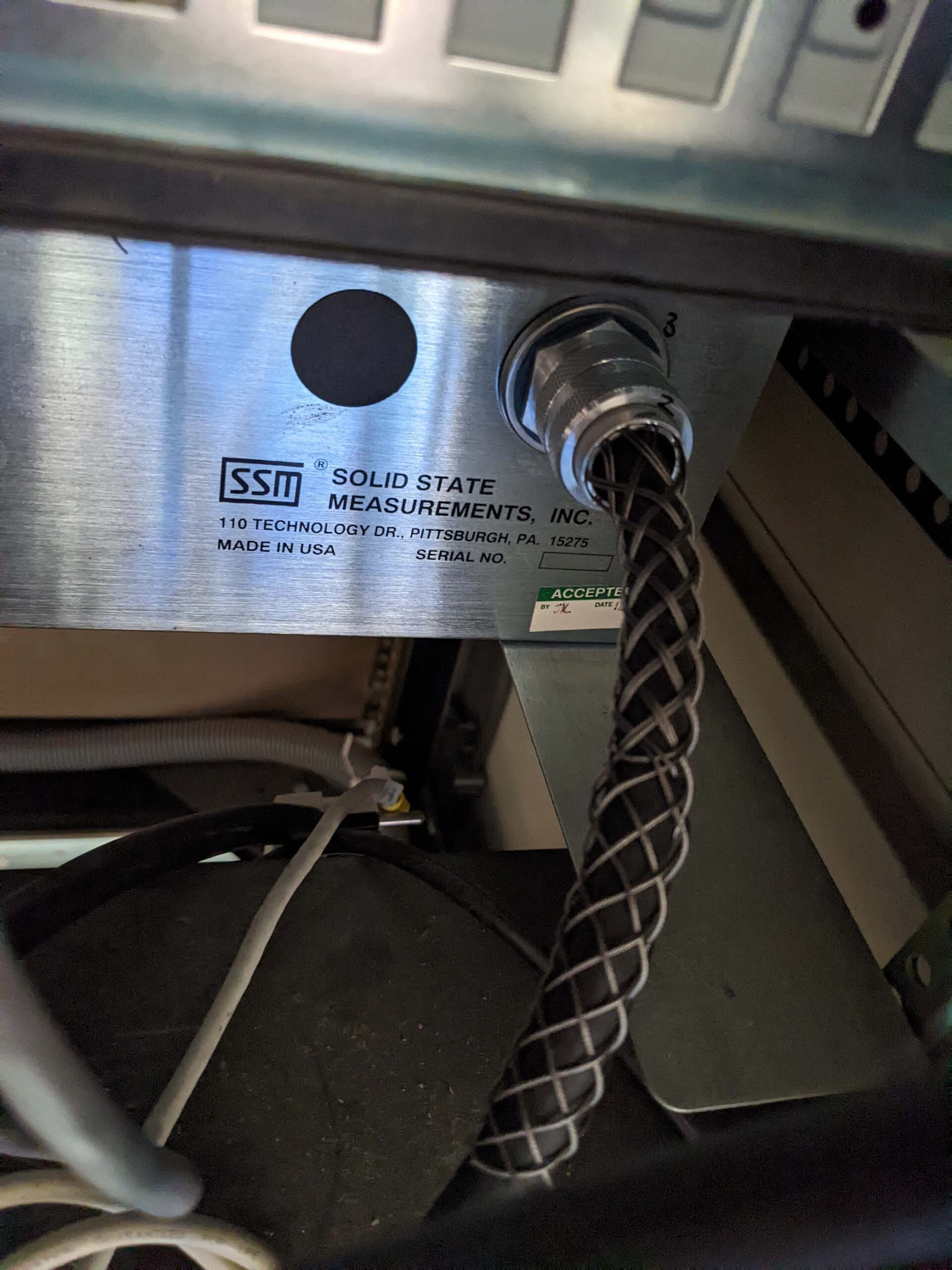
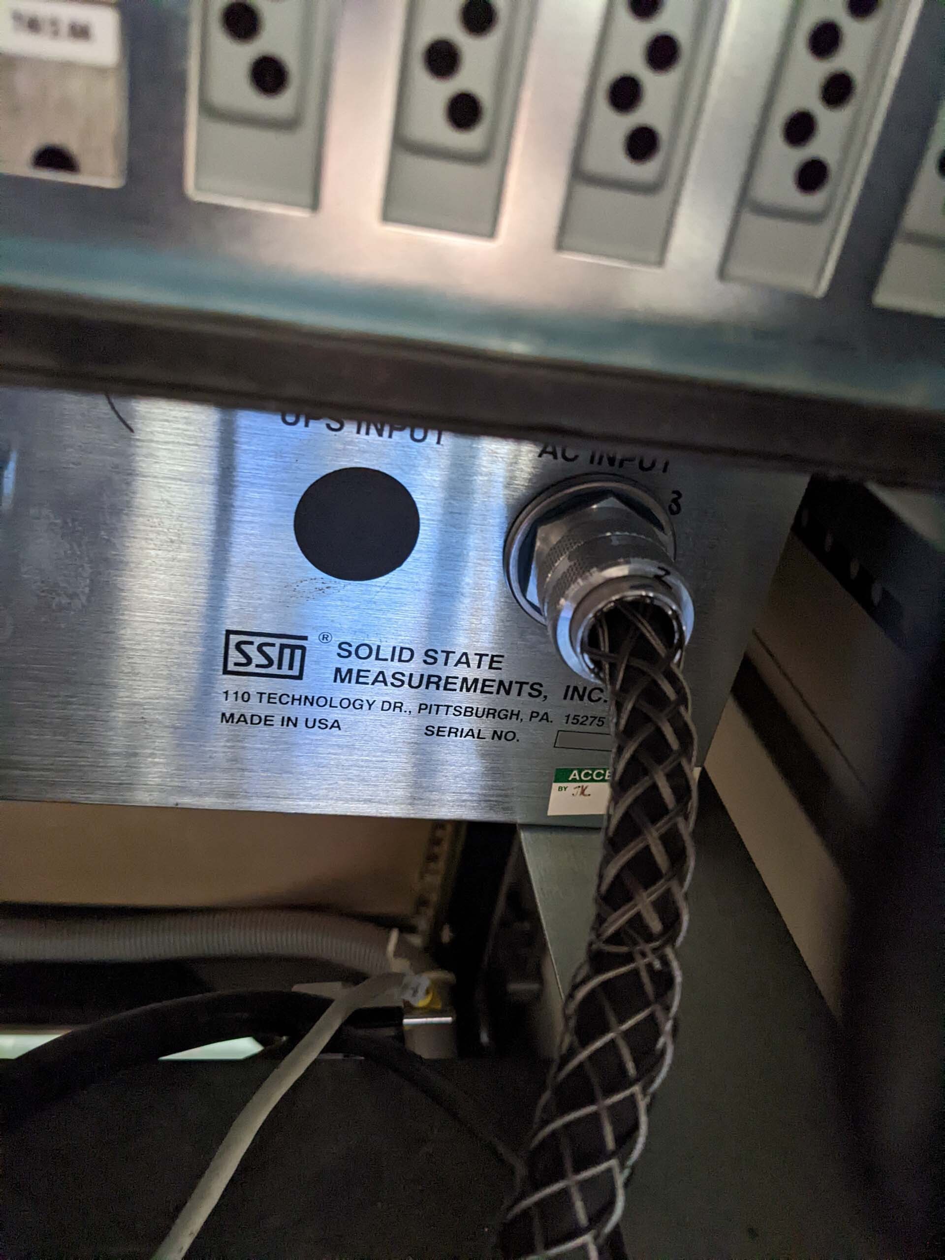
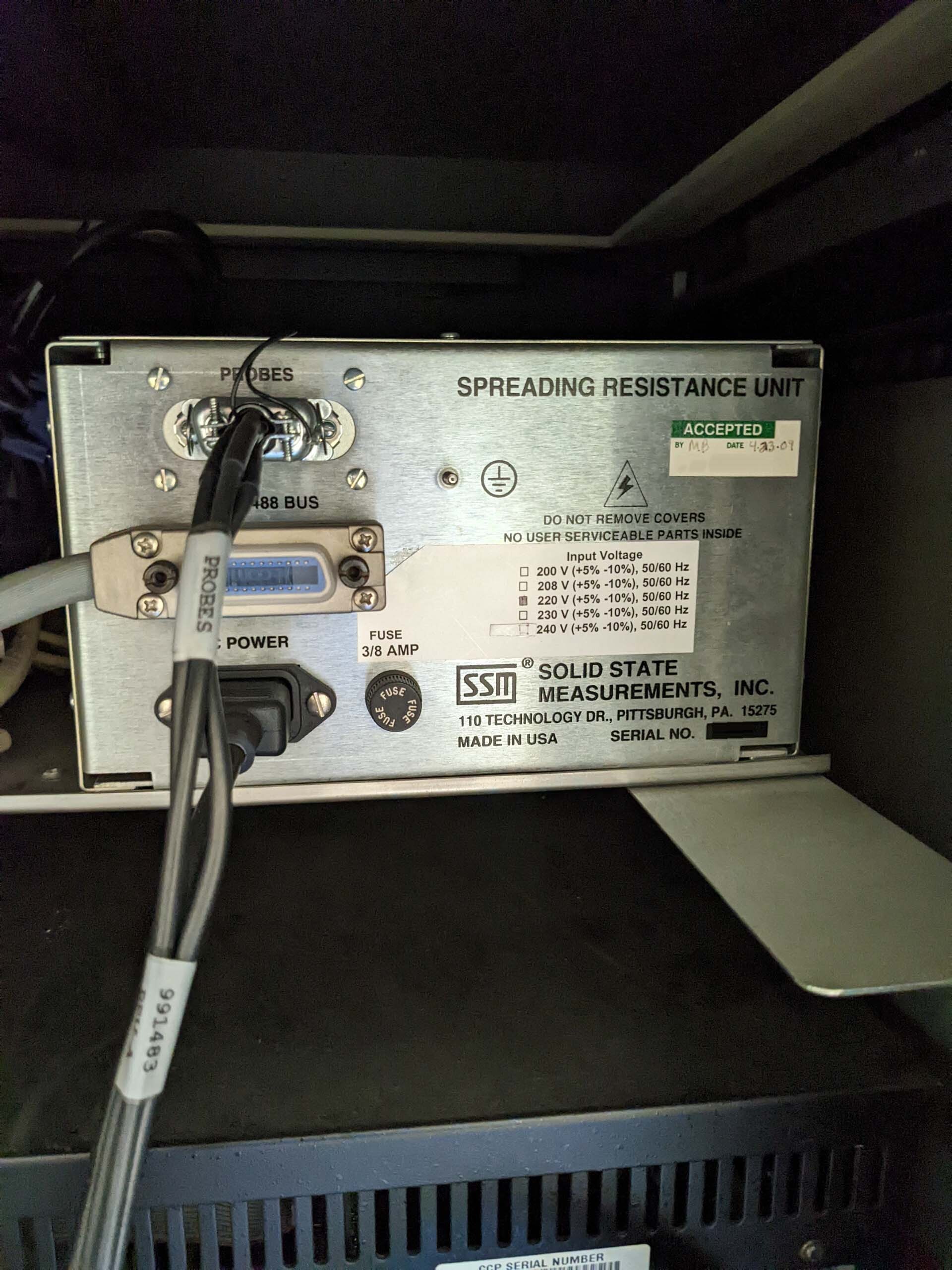
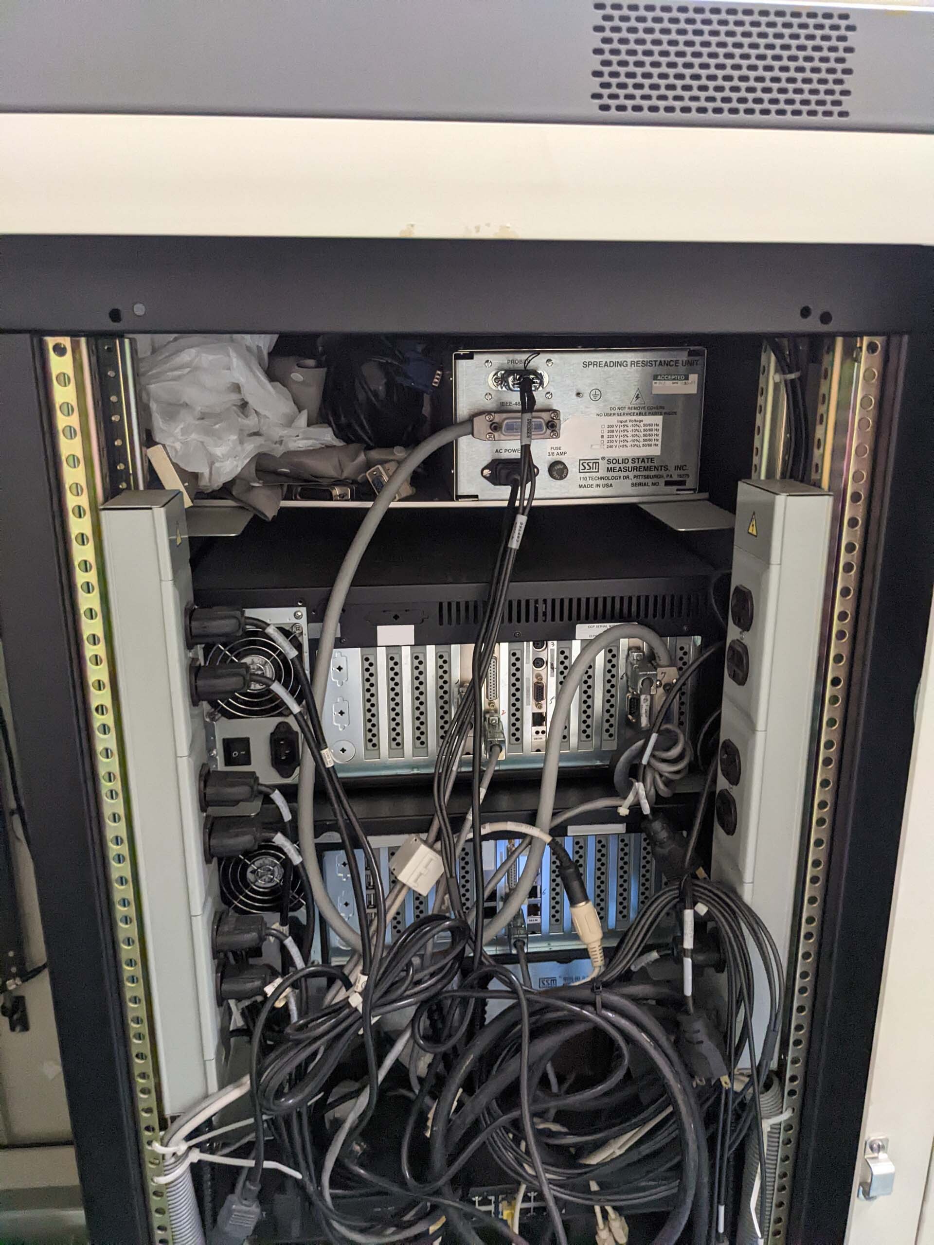
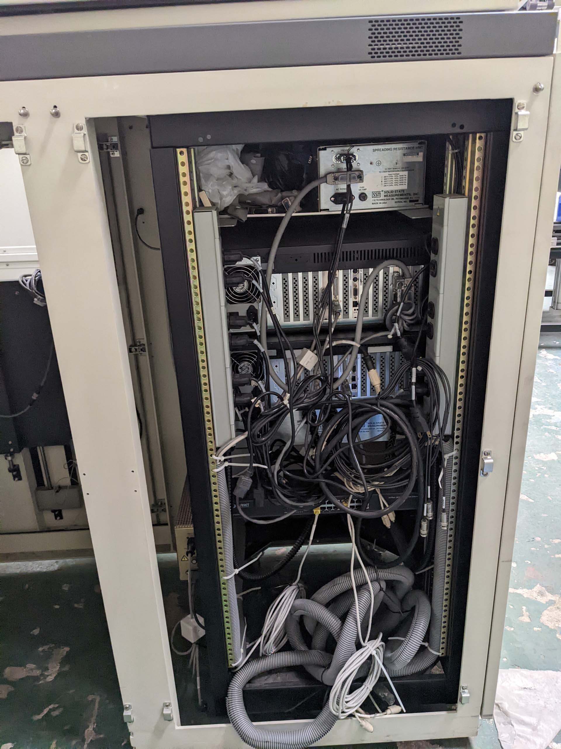
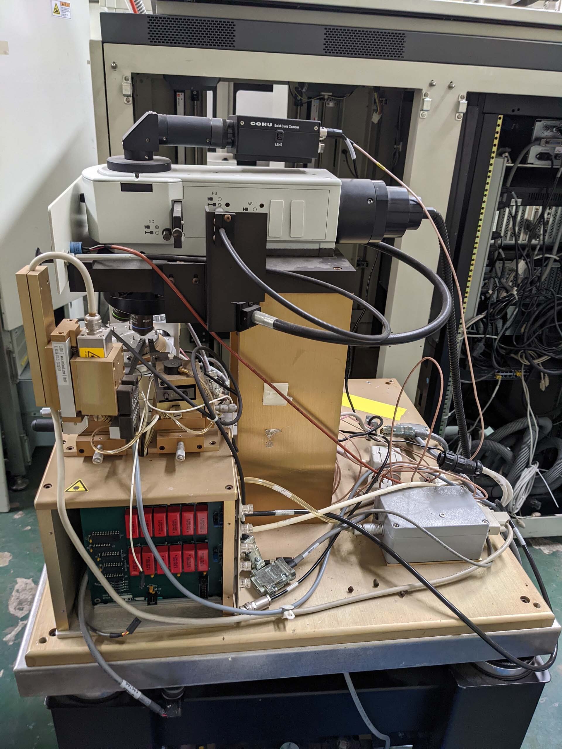

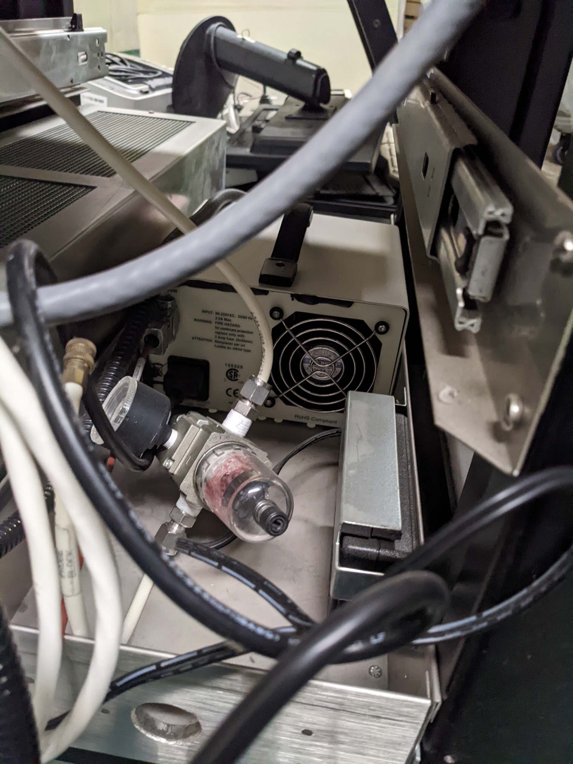
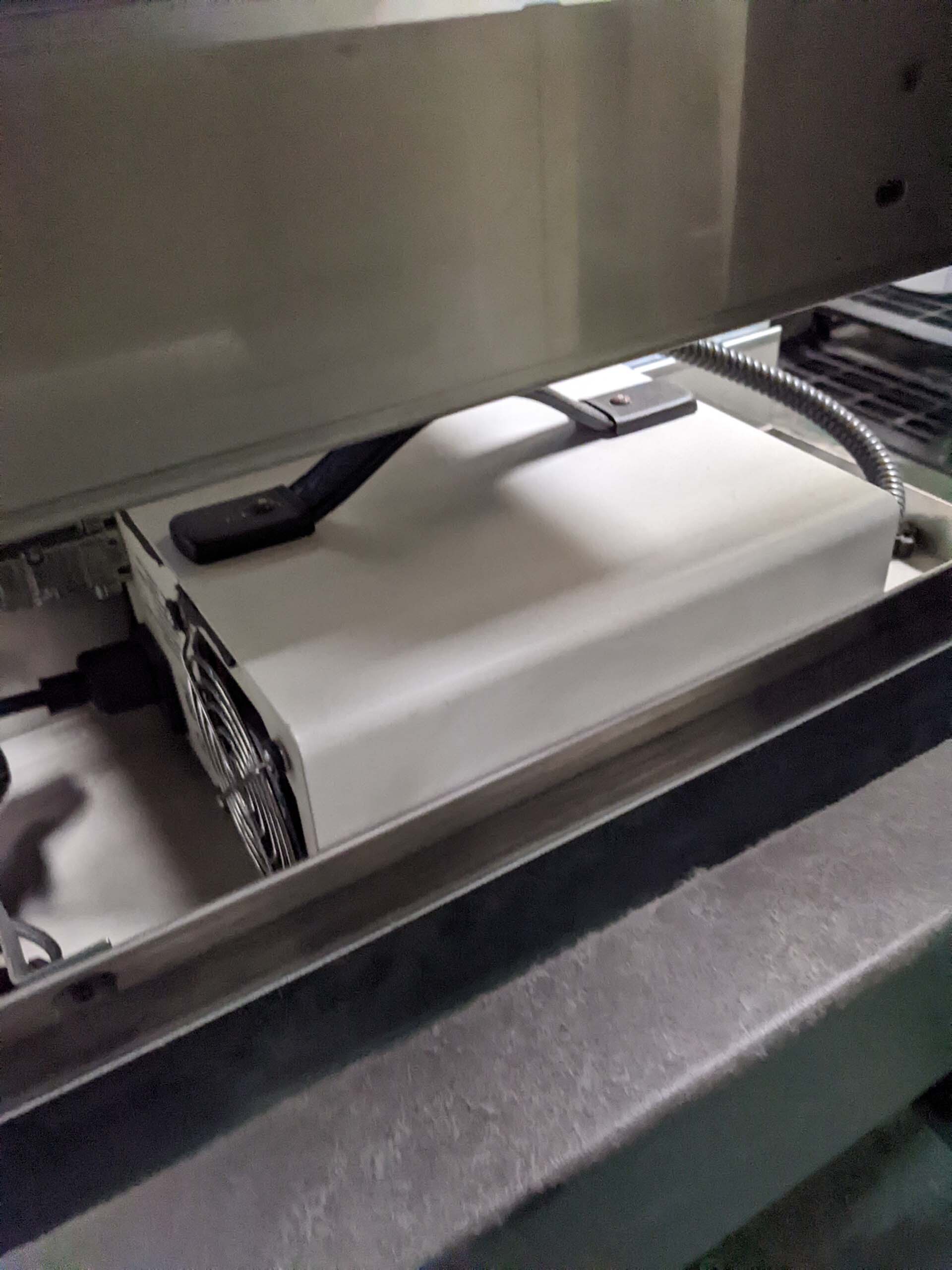
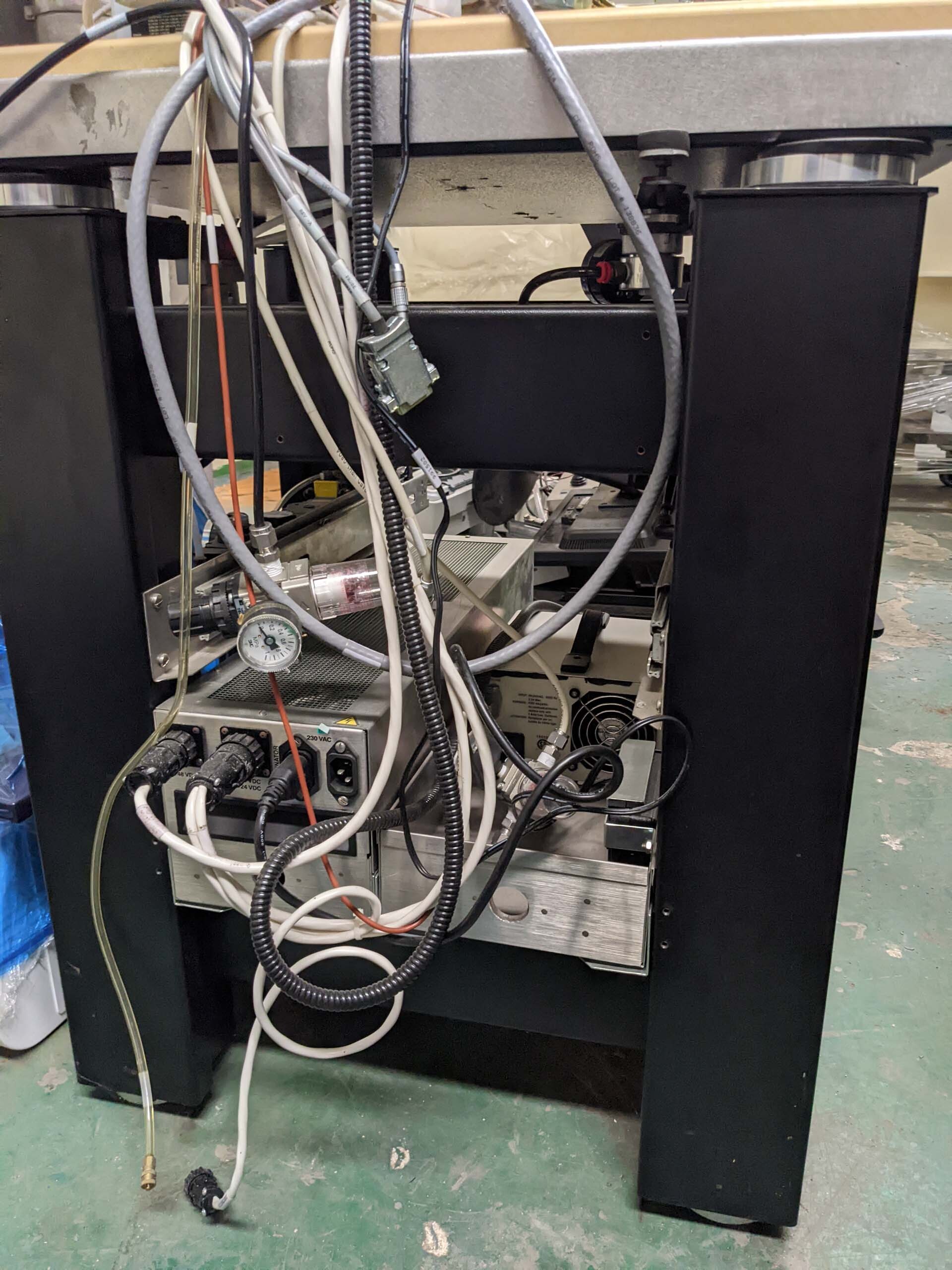
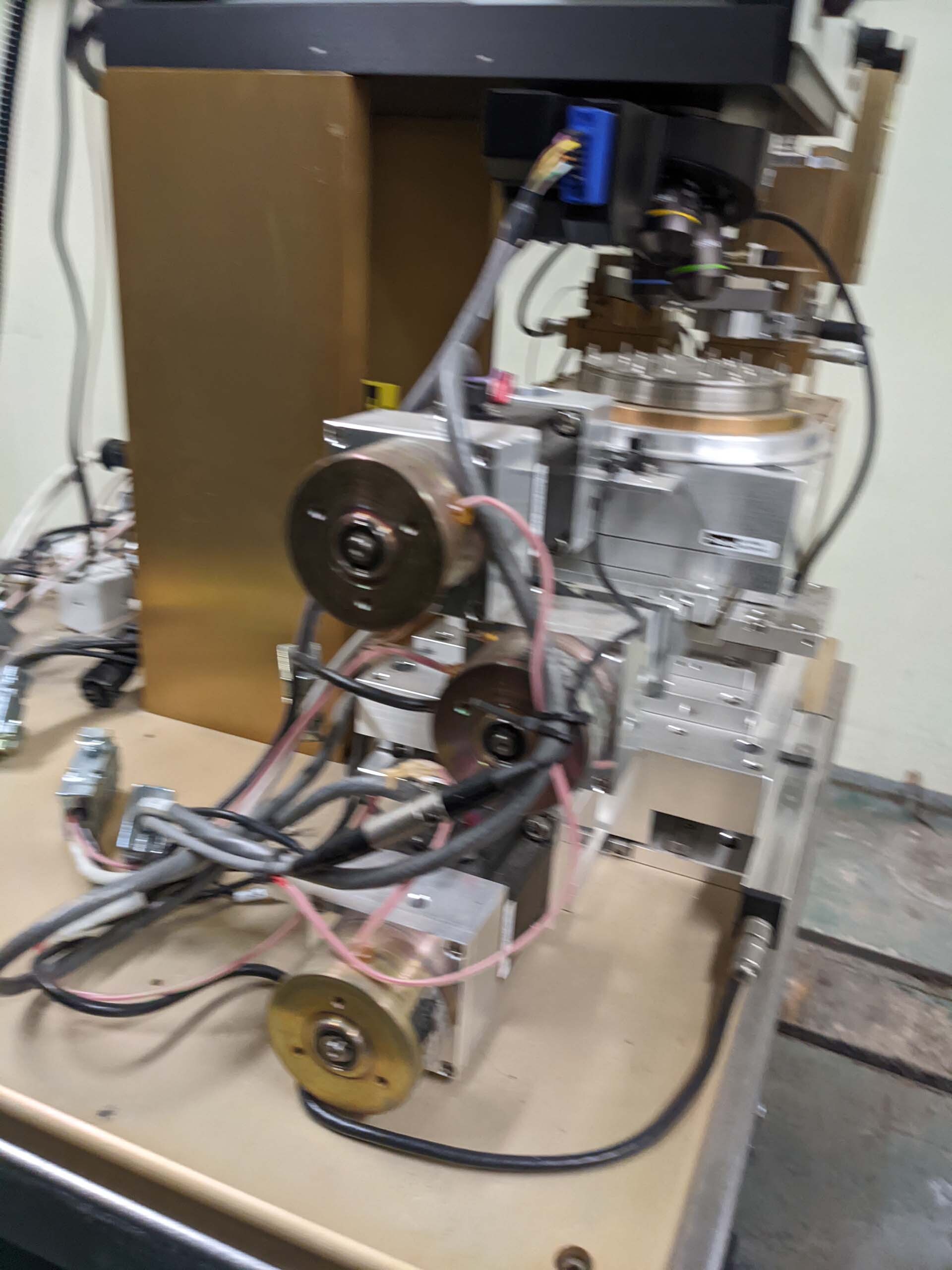
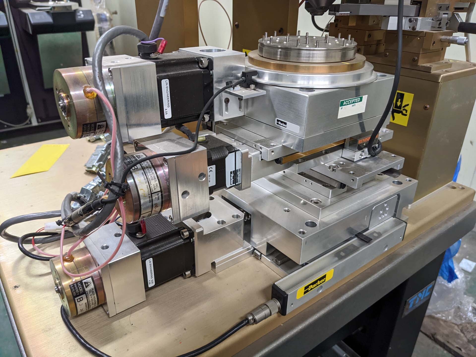
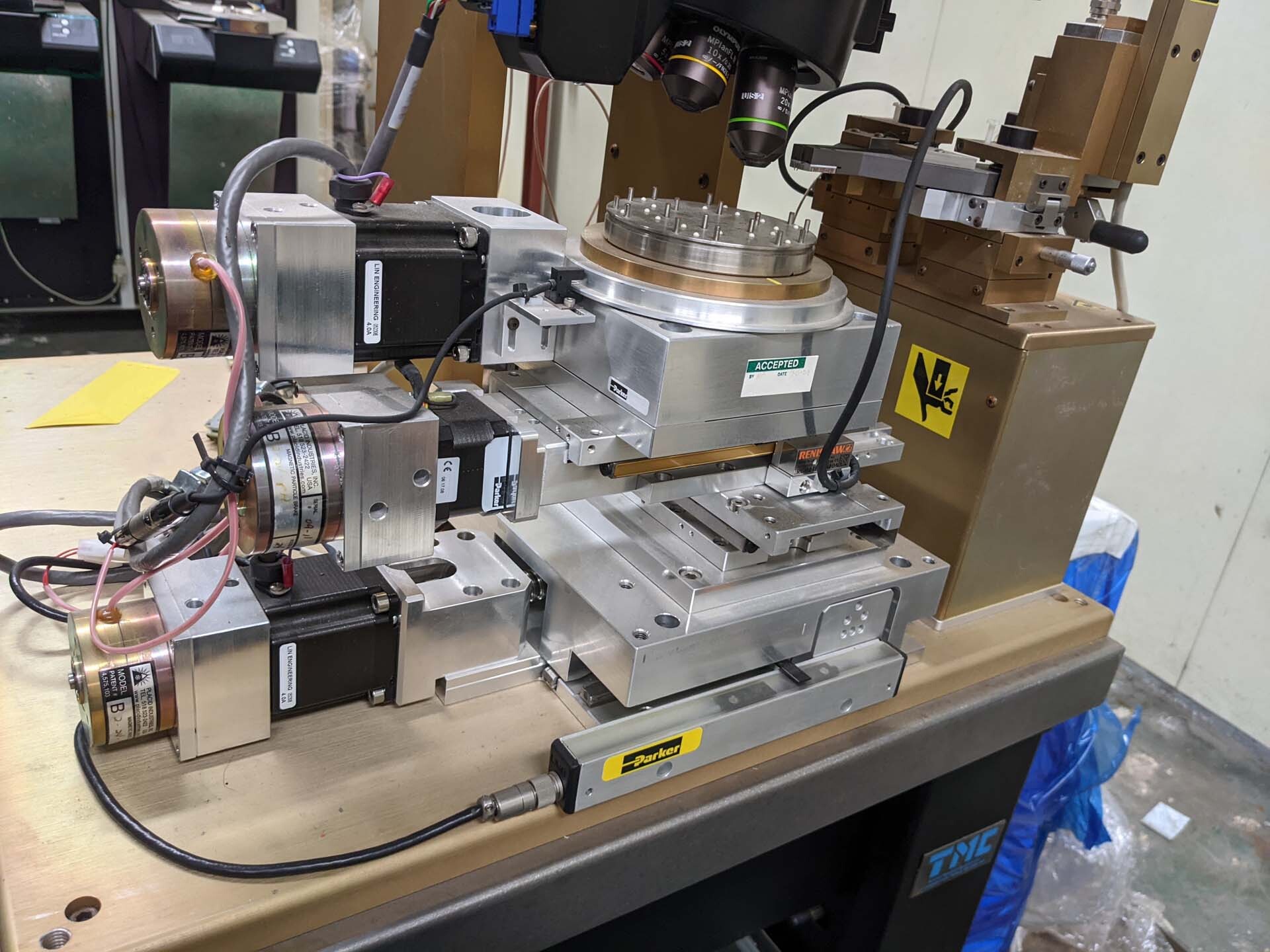
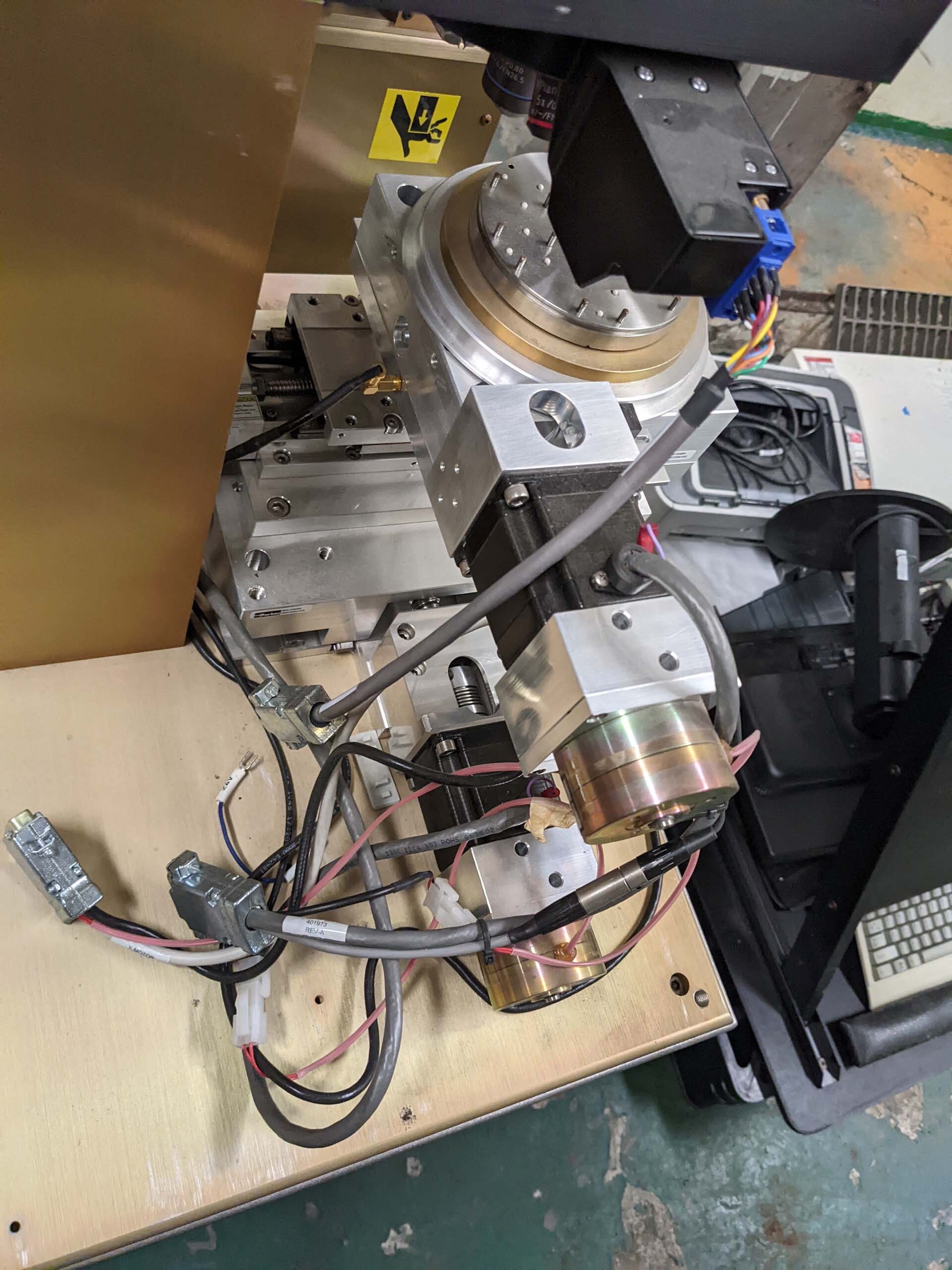
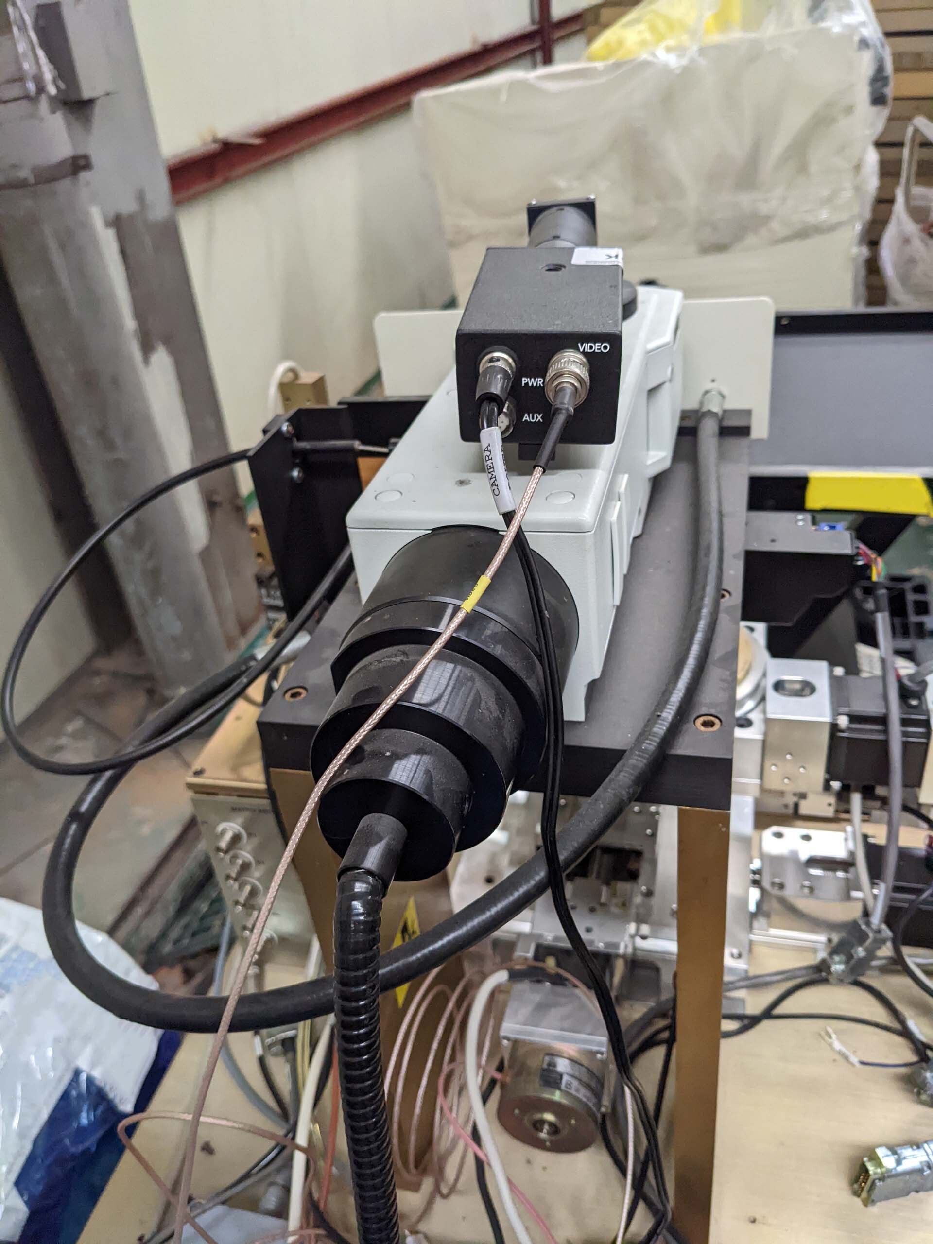
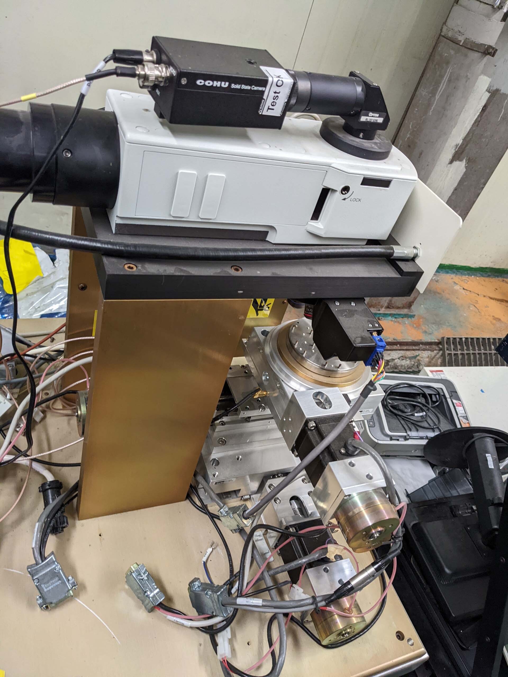
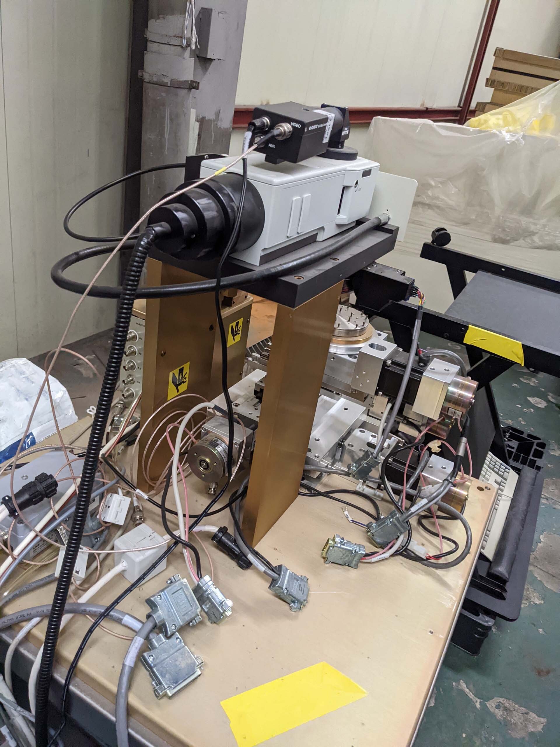
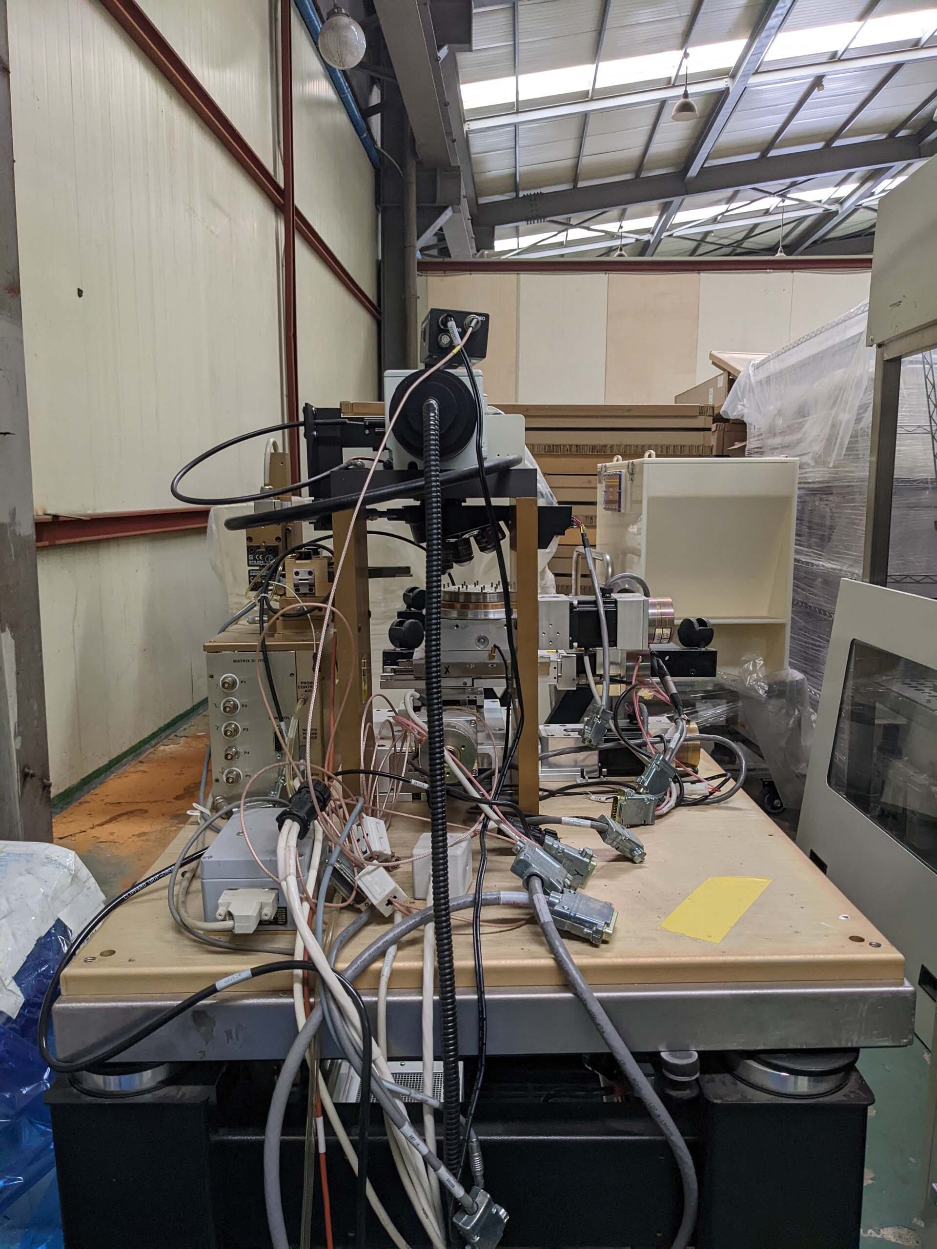
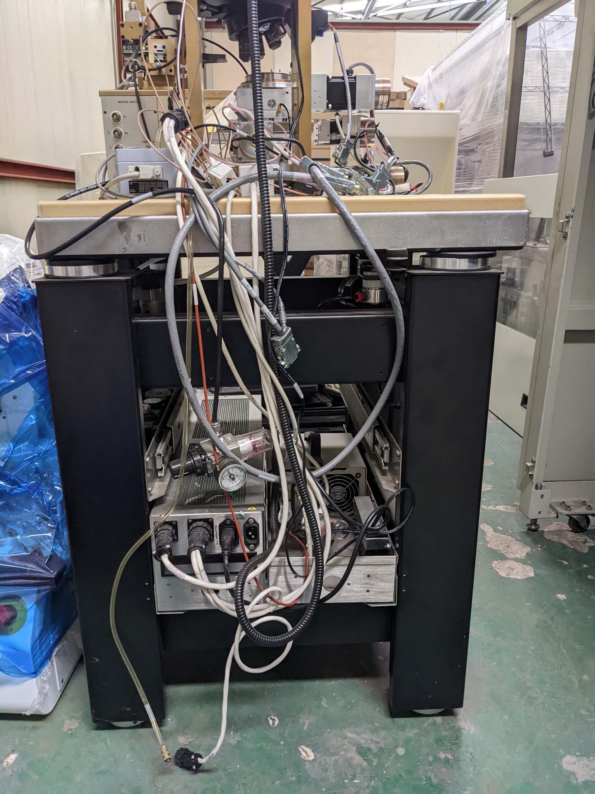
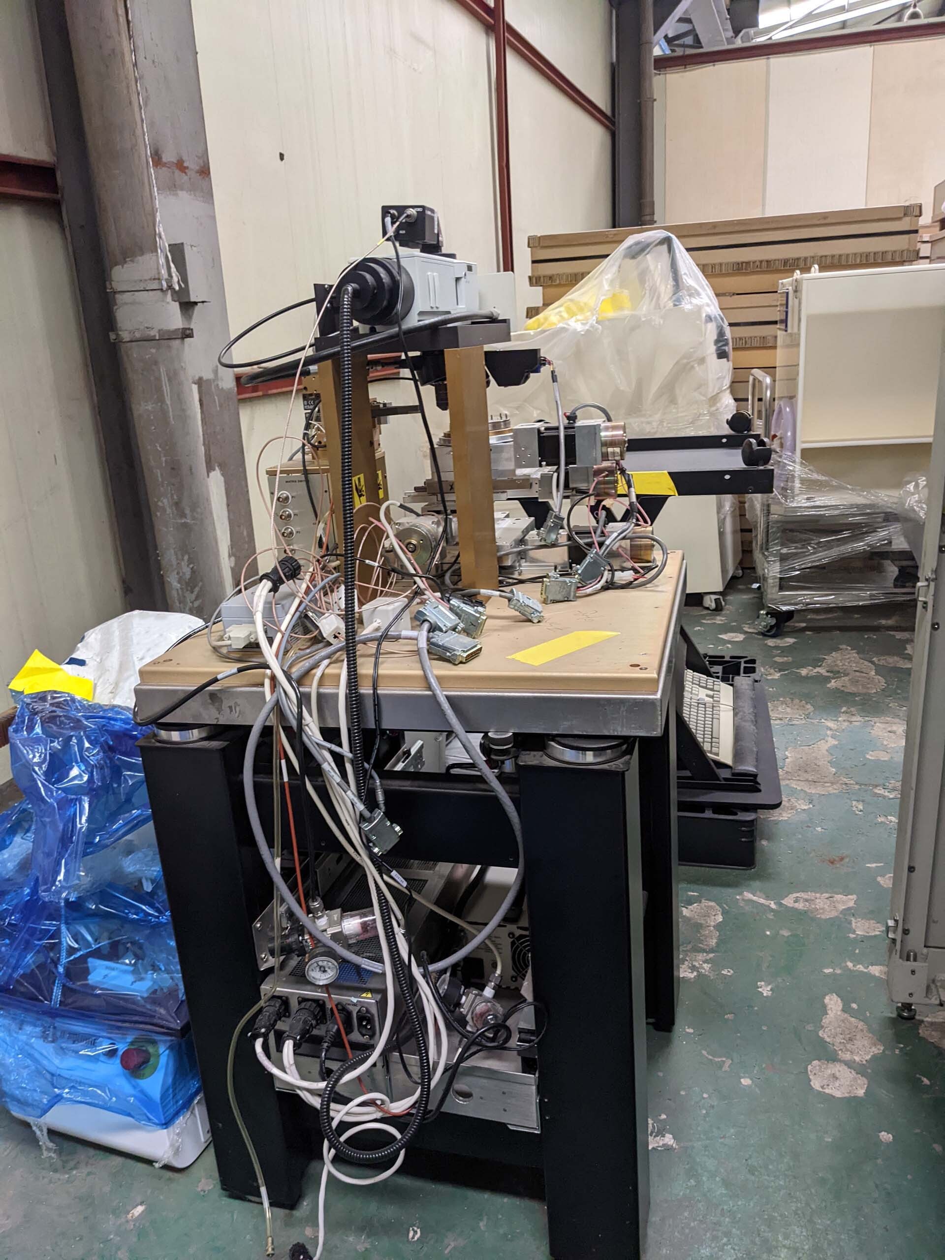
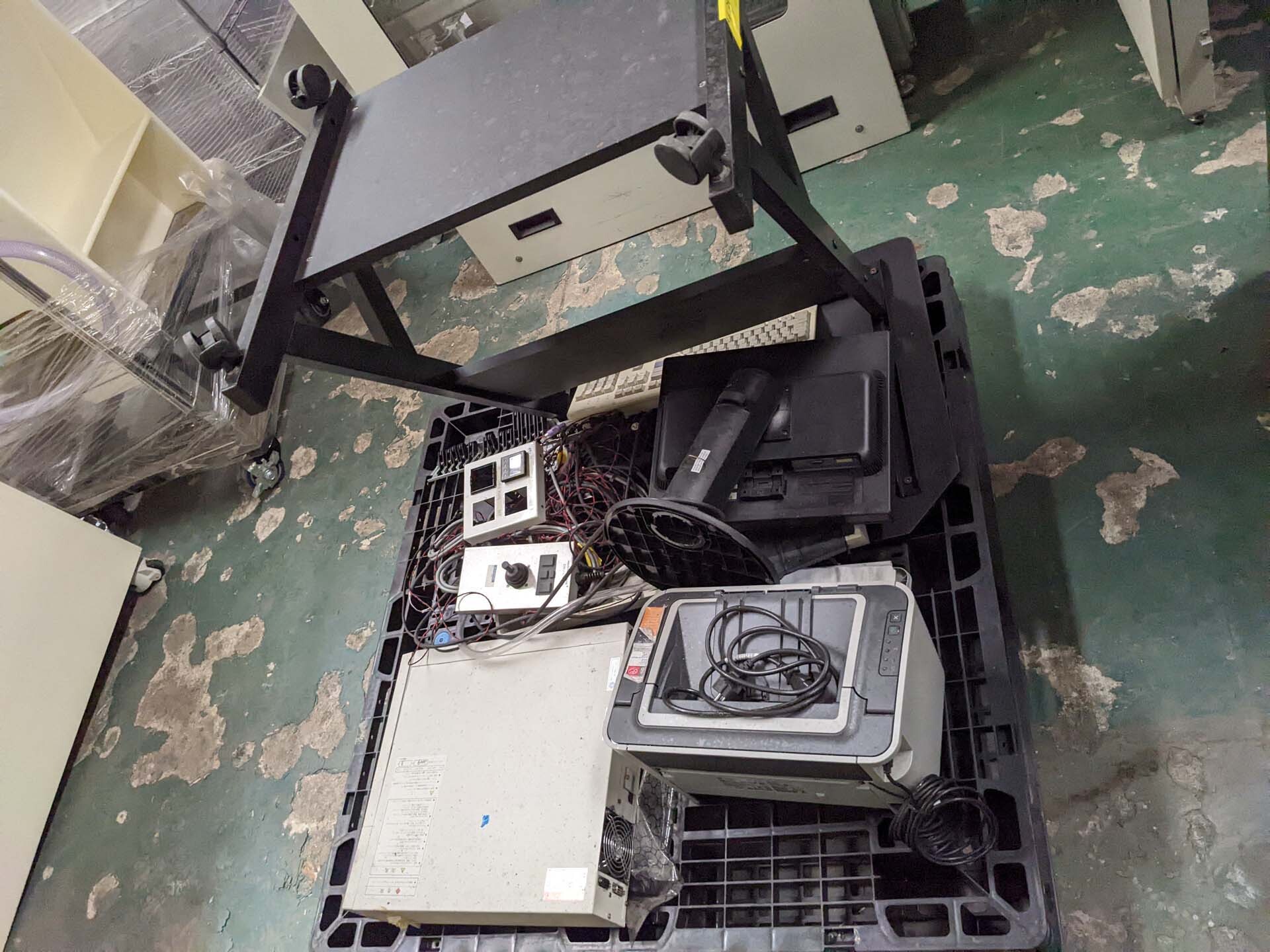
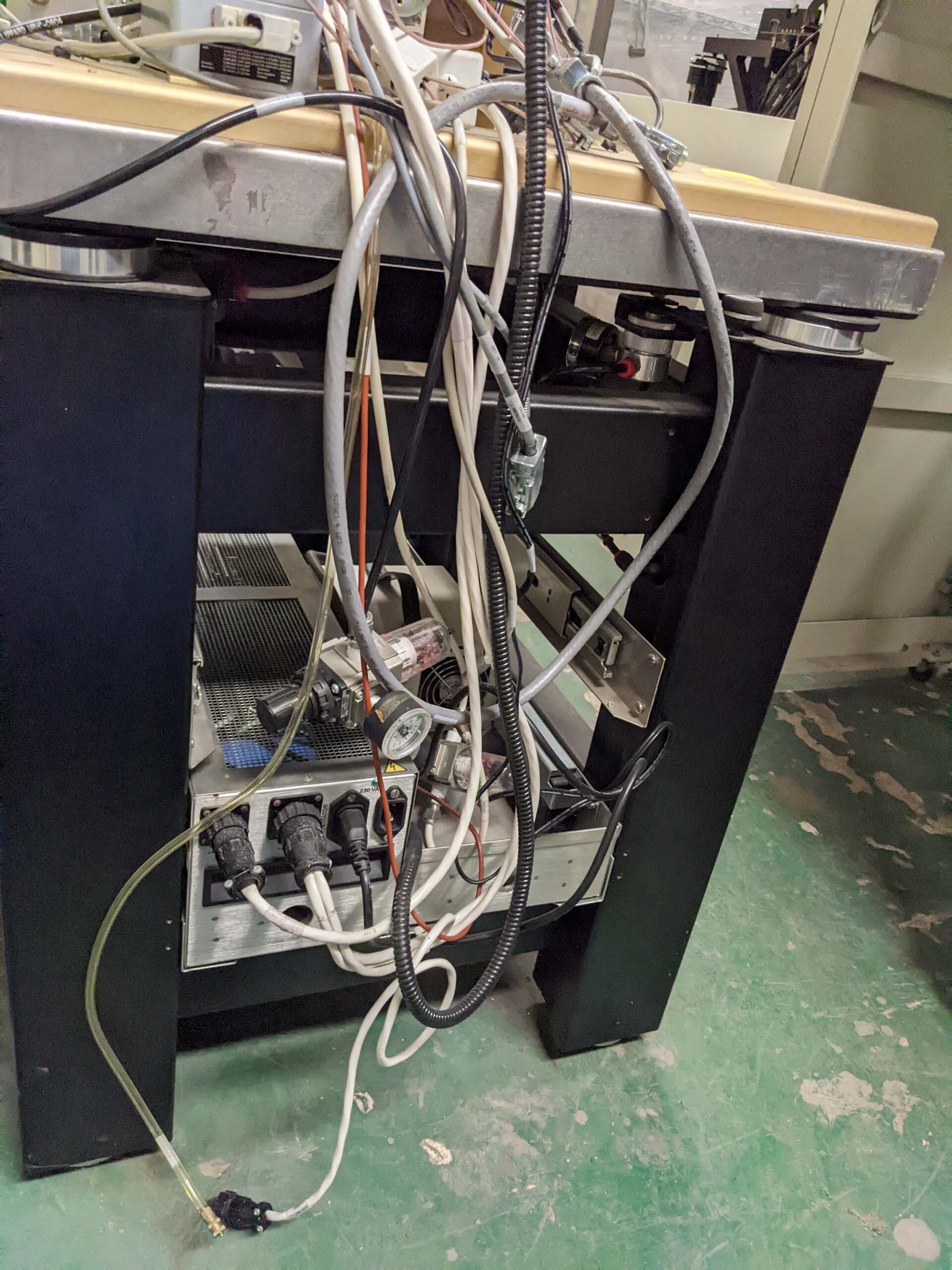
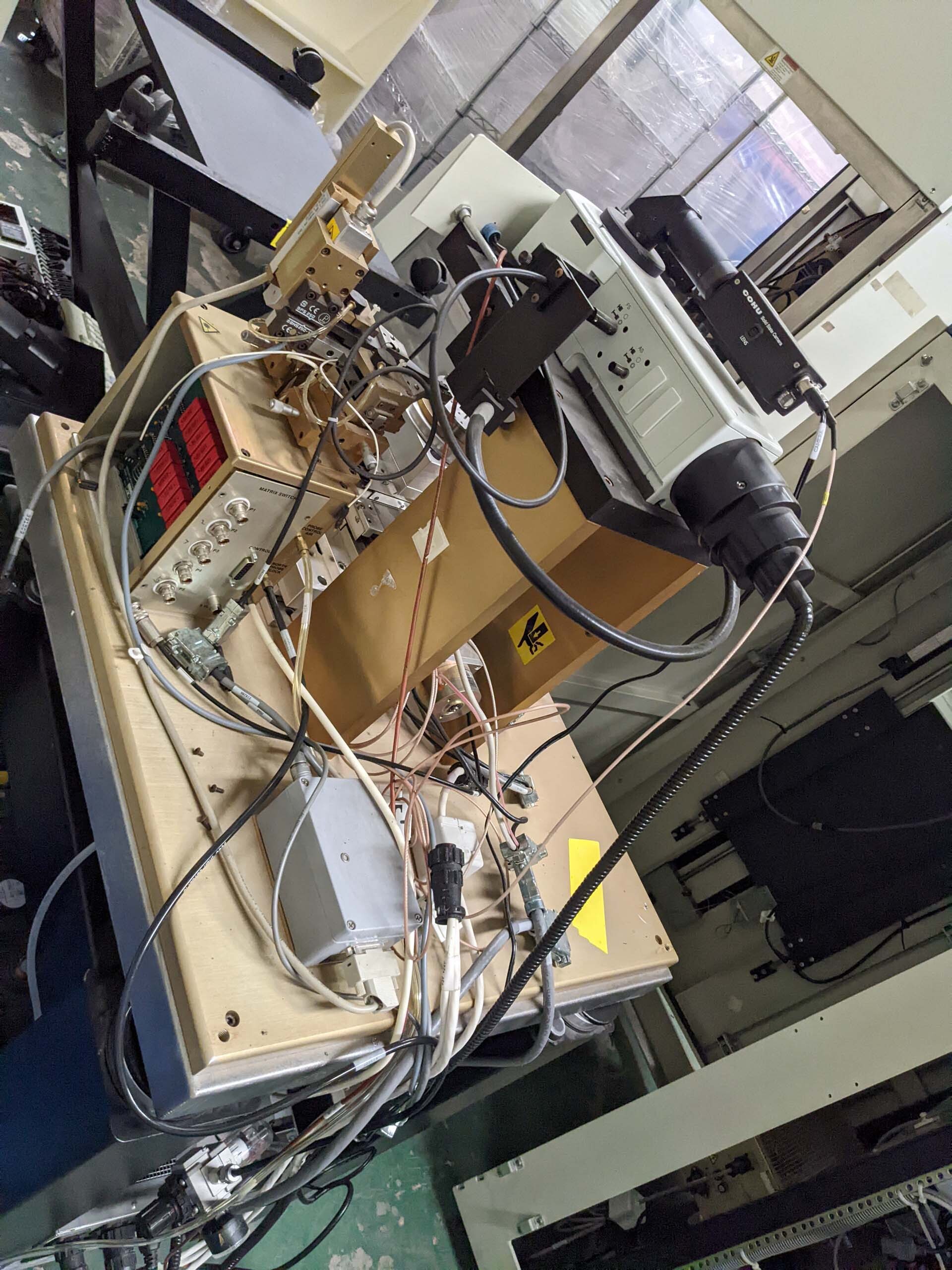
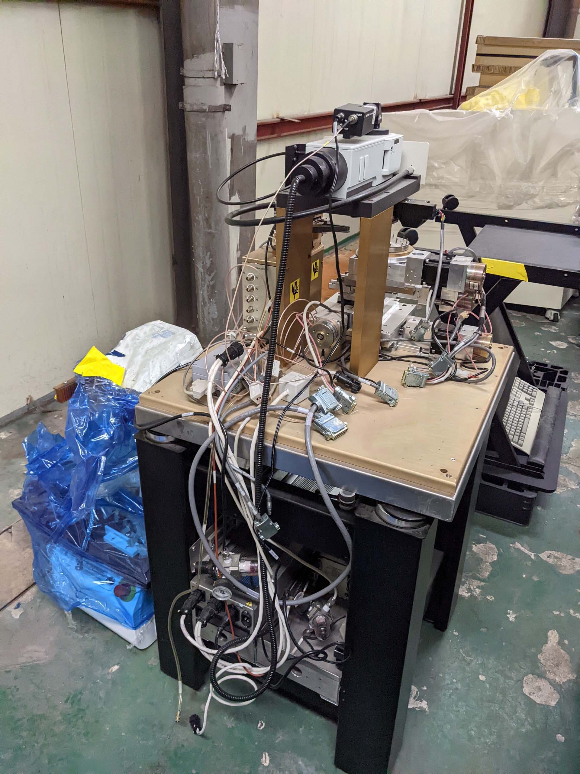
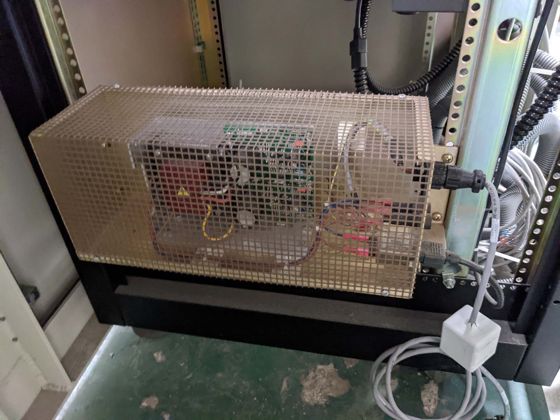
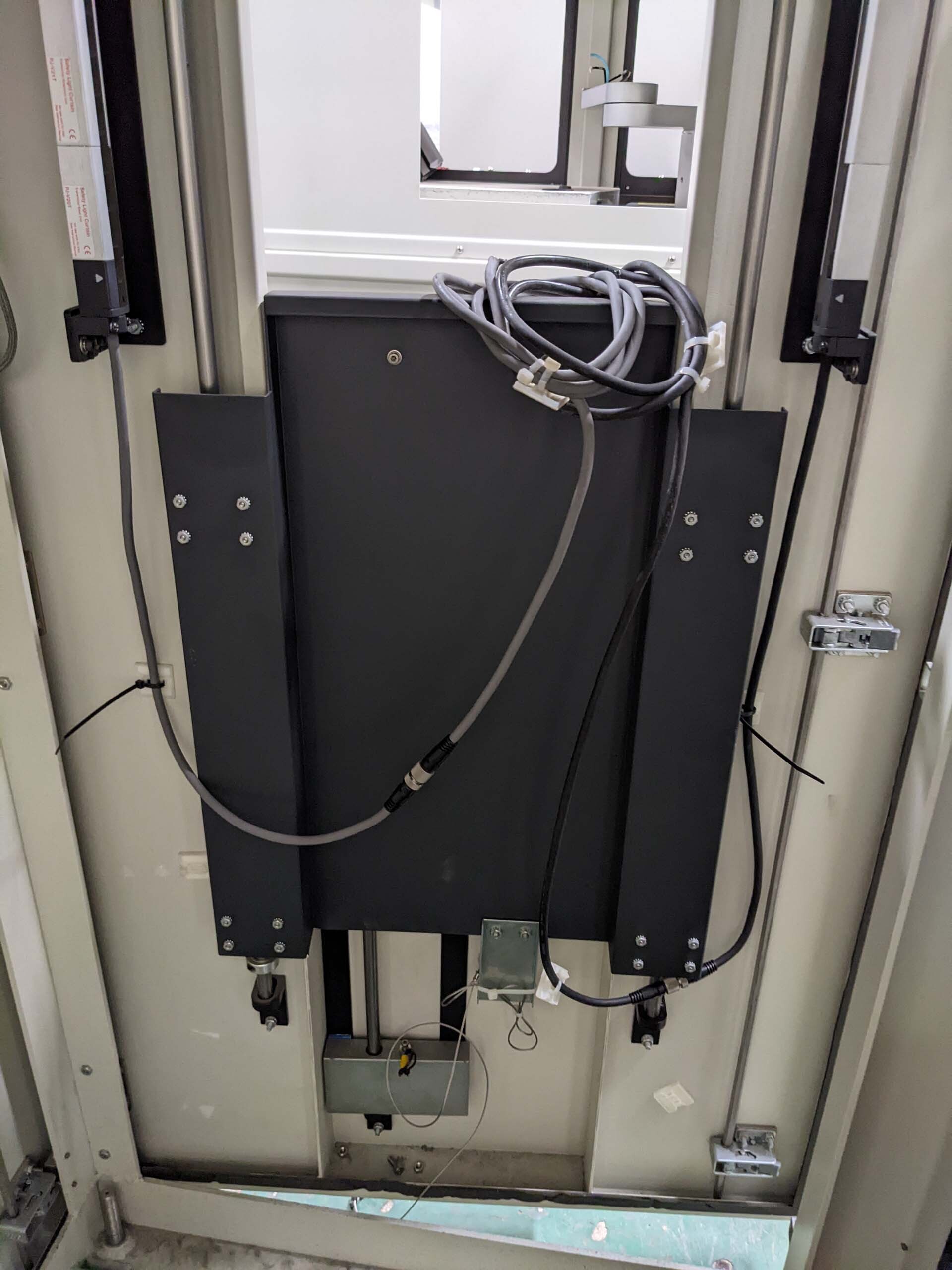
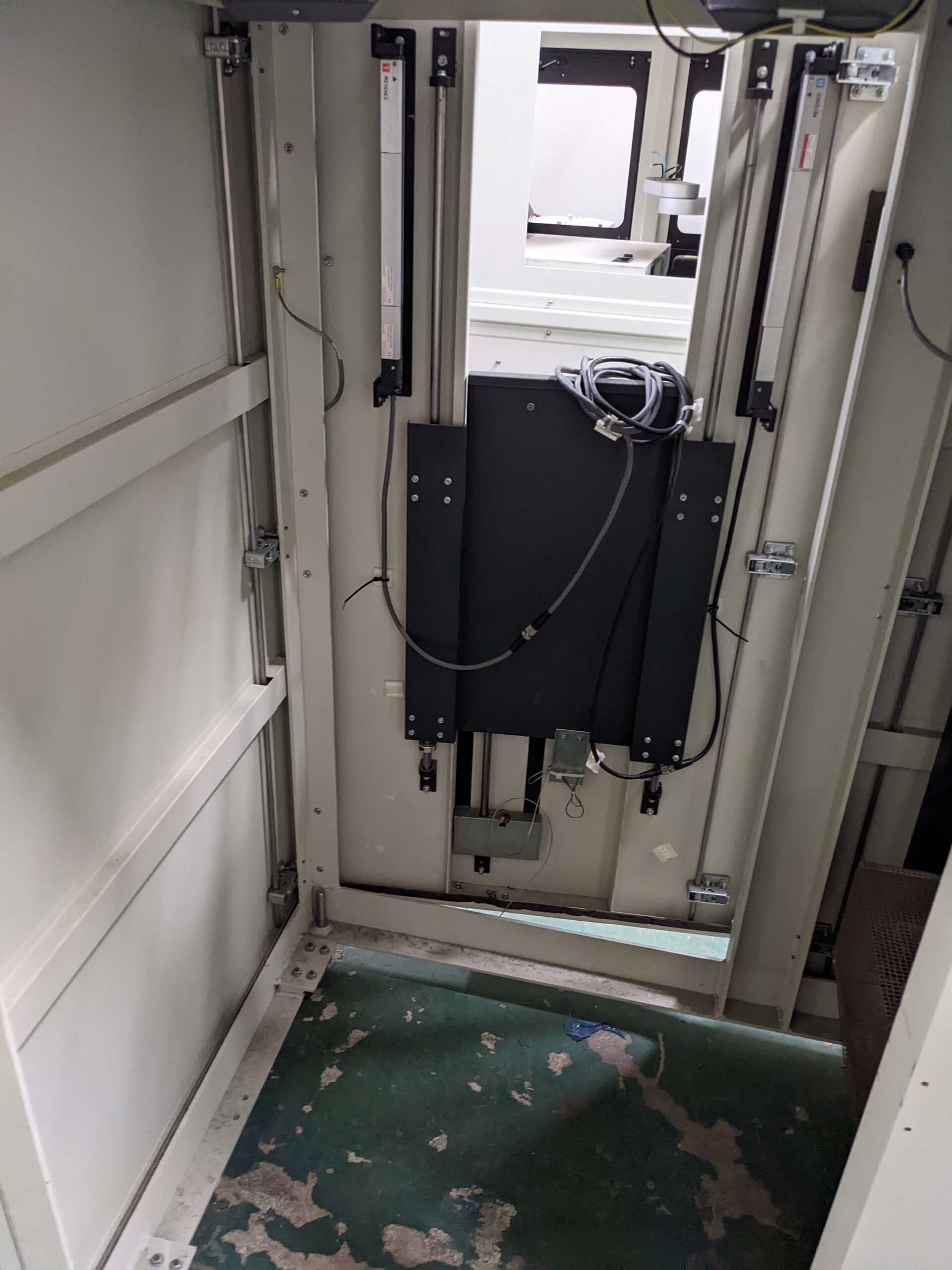
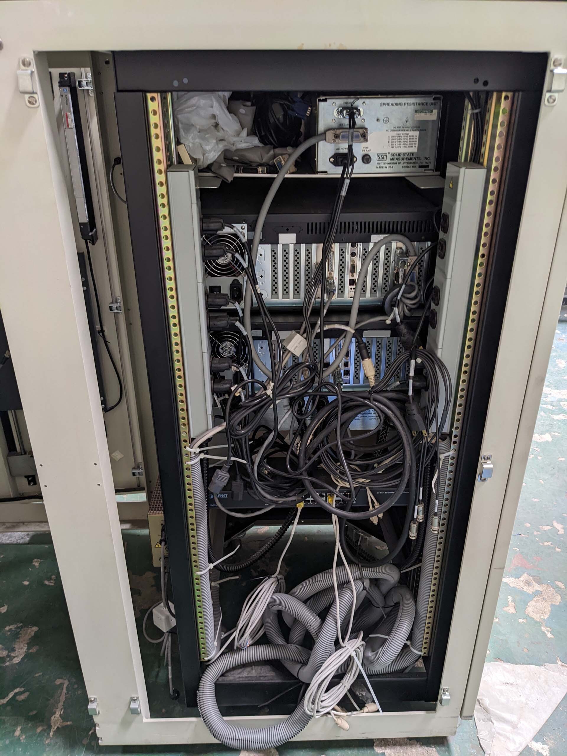
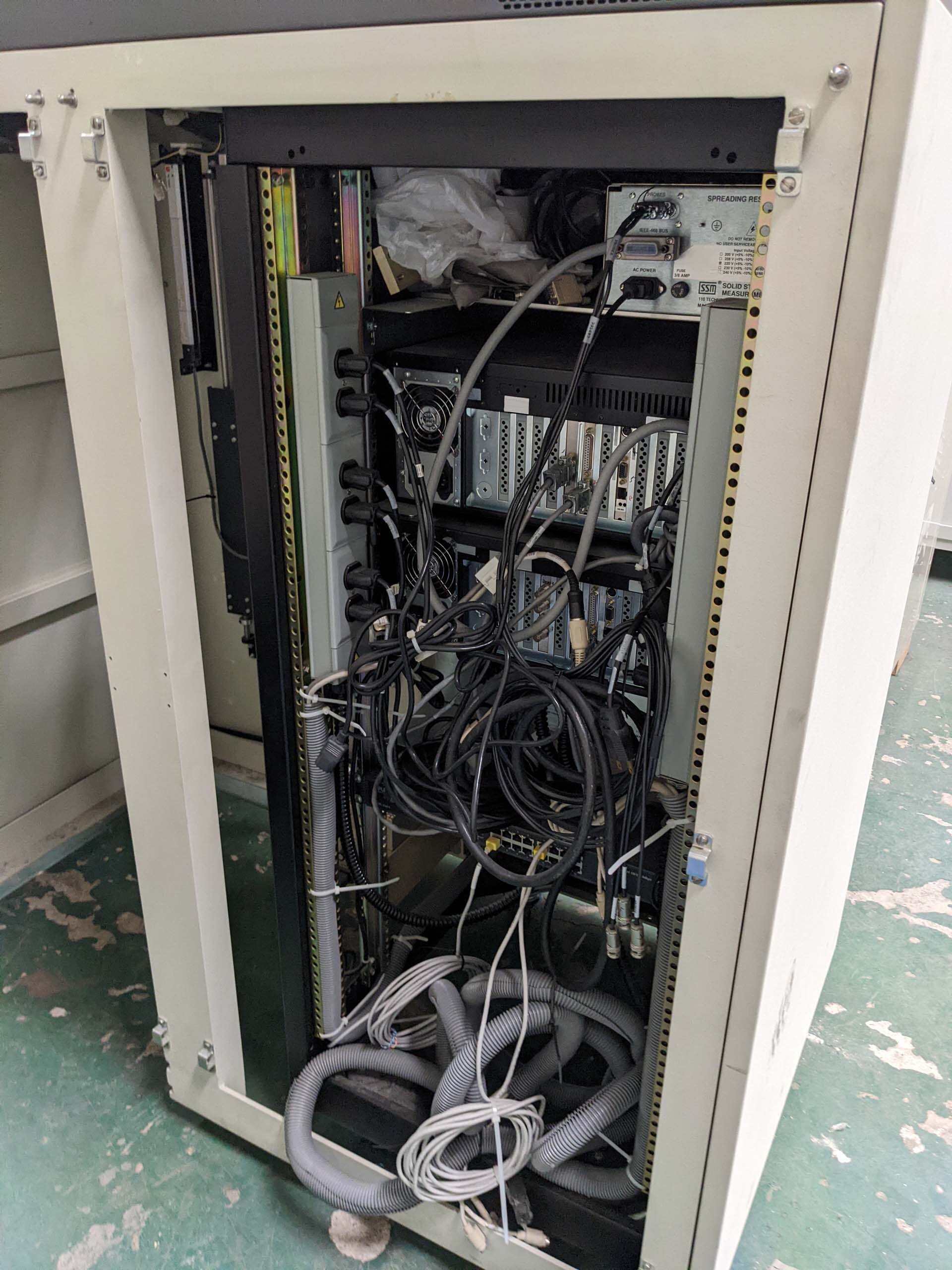
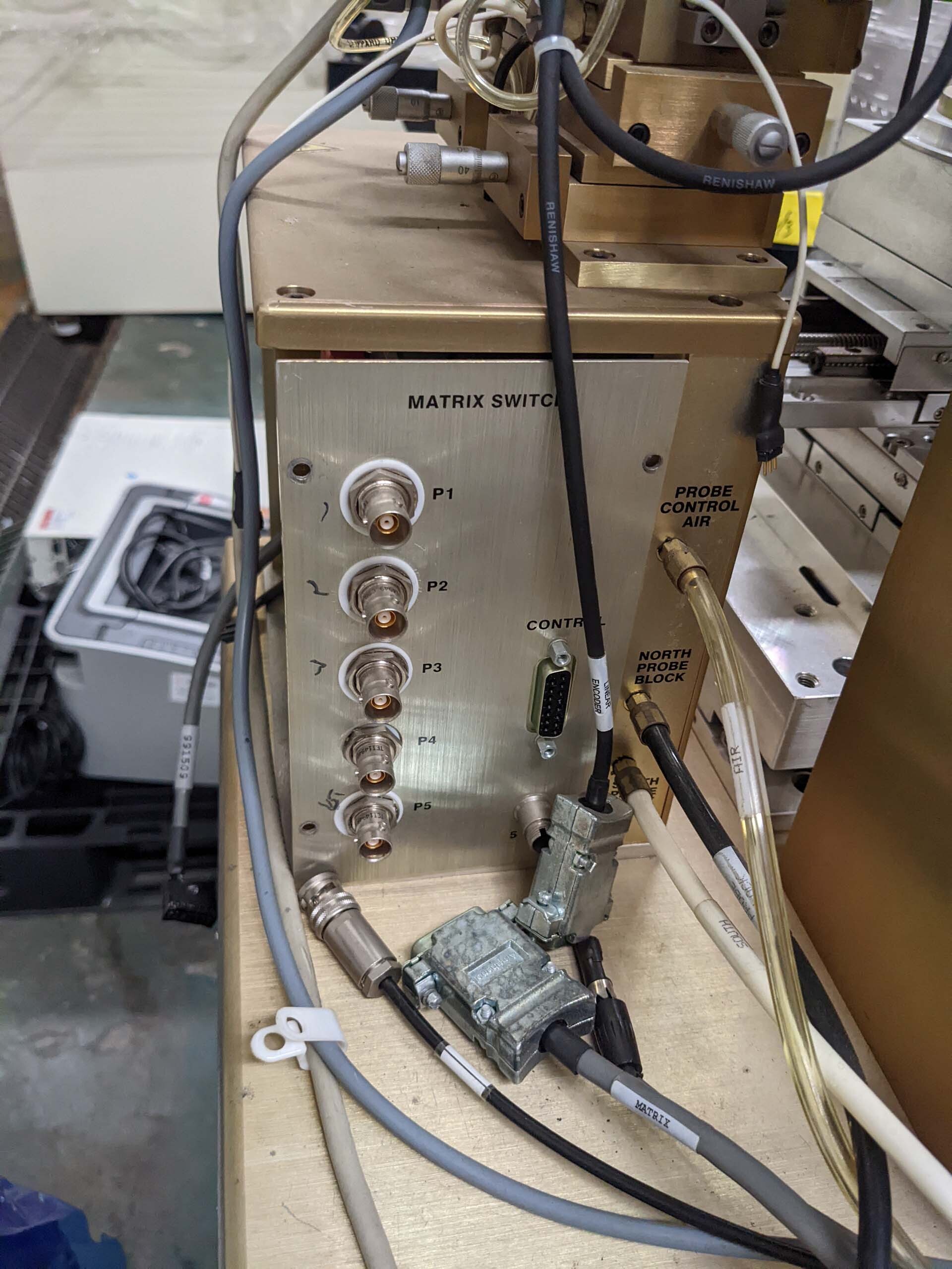
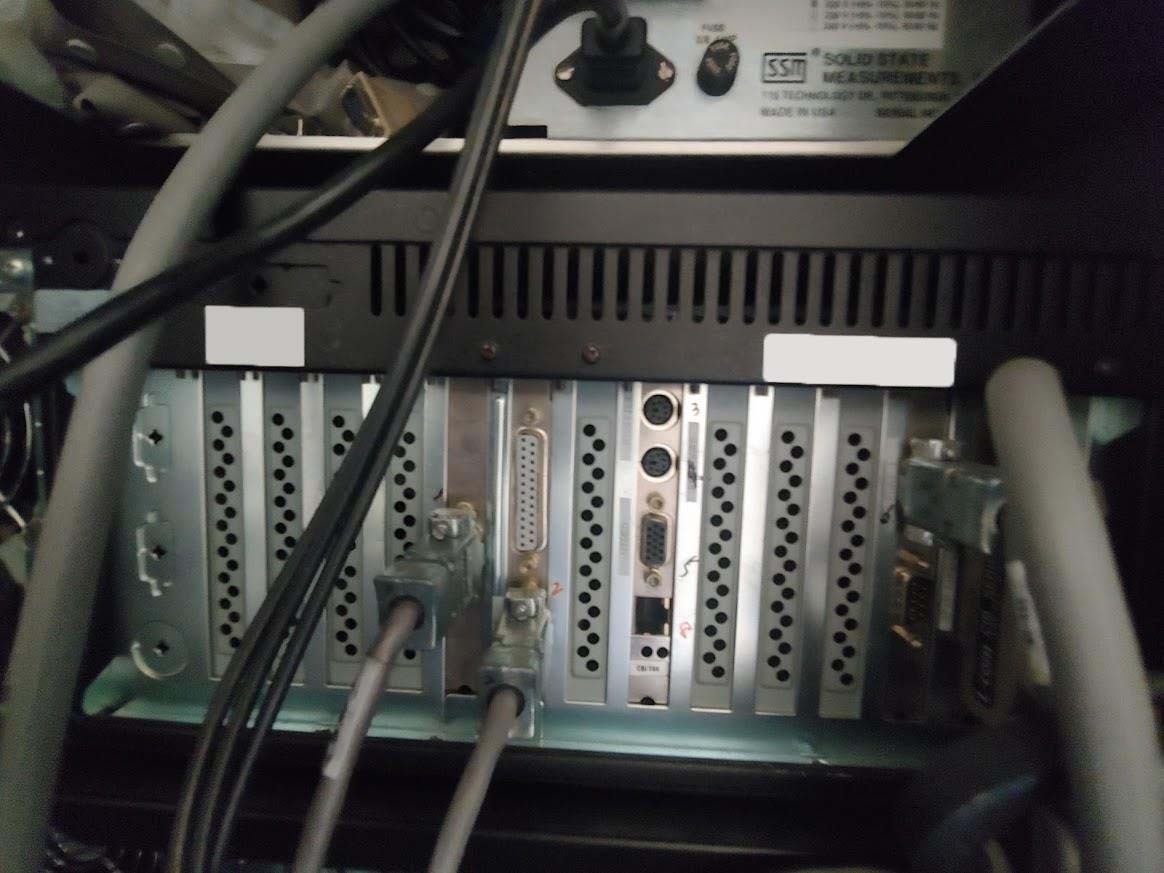
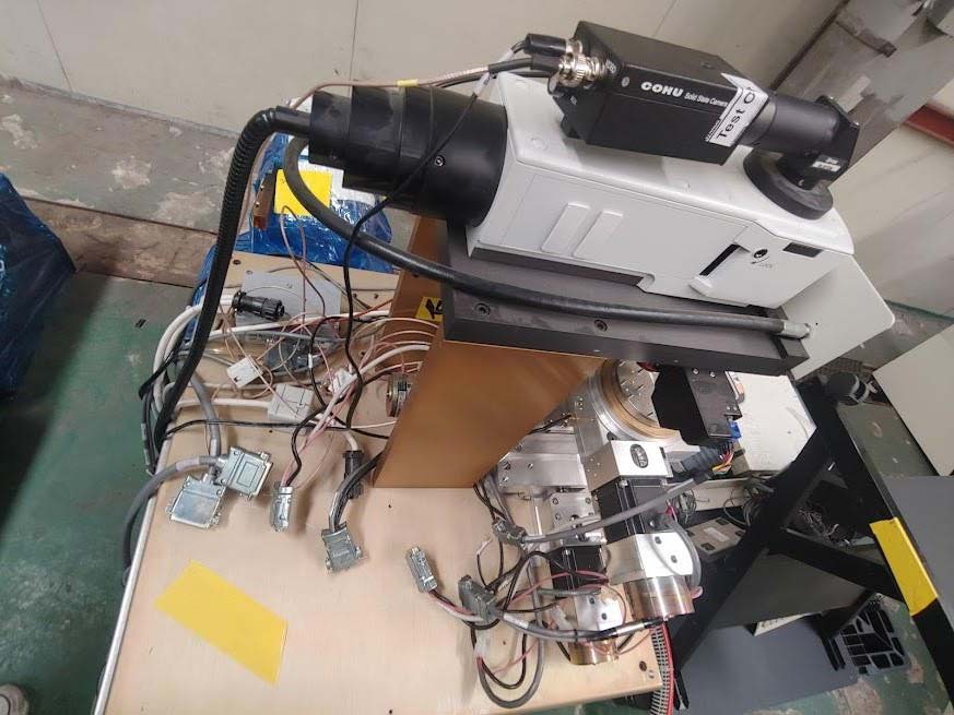
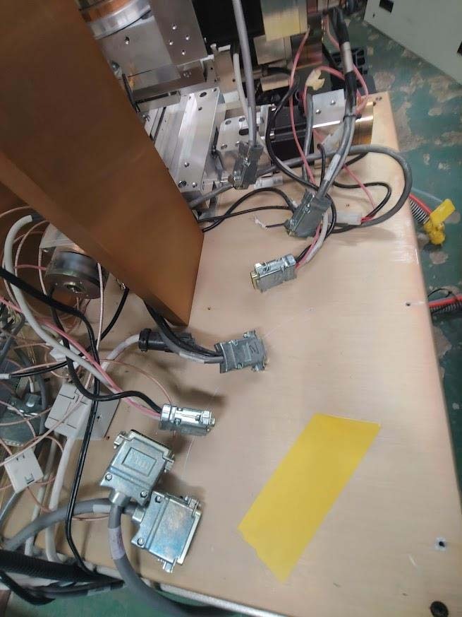
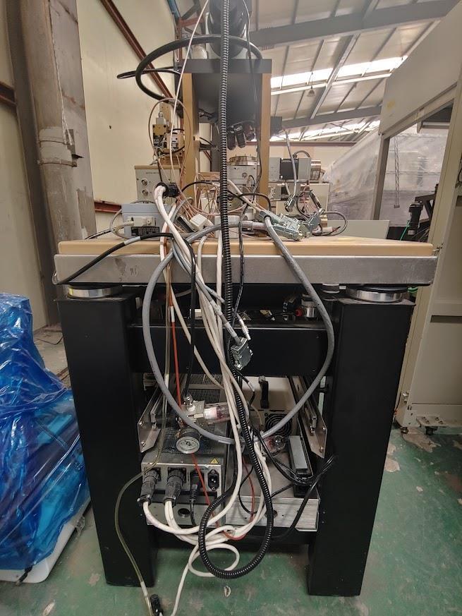
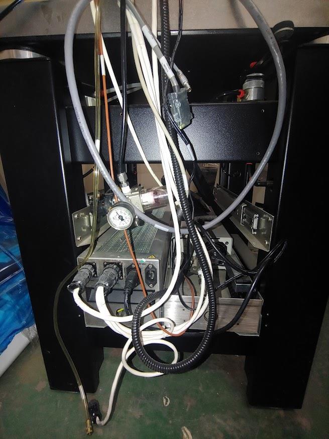
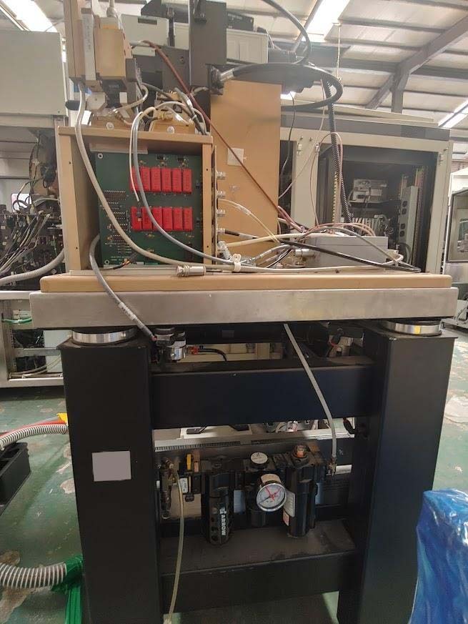
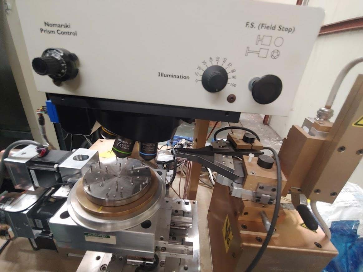
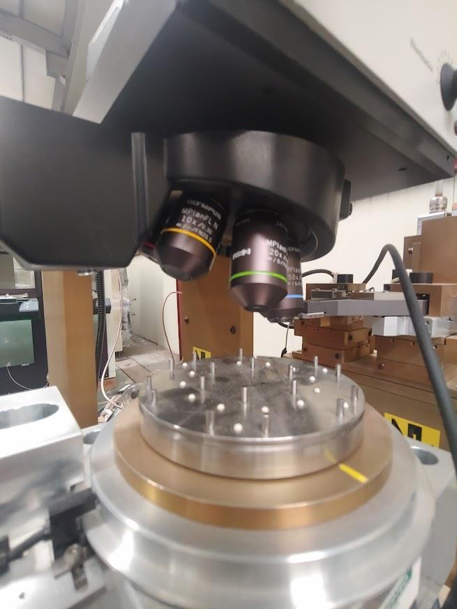


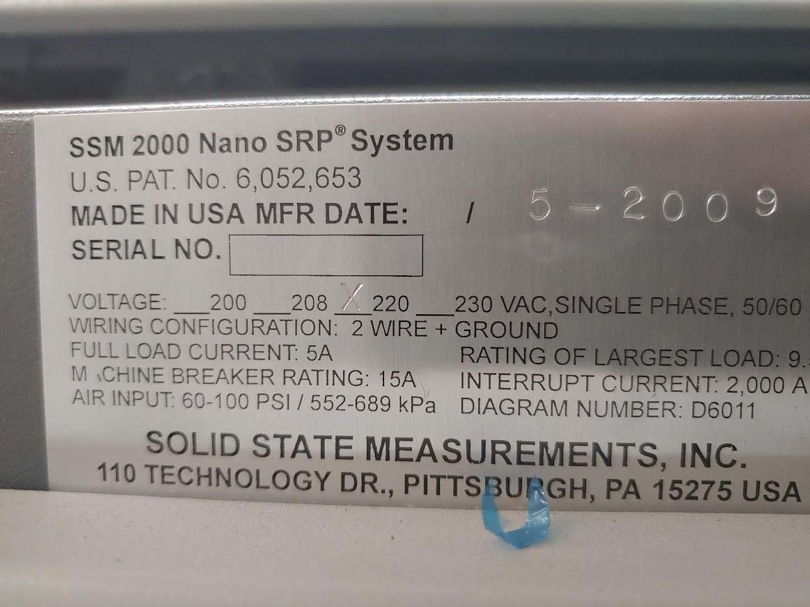
ID: 293665614
Vintage: 2009
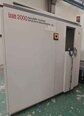
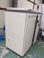
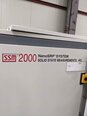
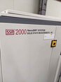
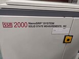
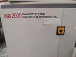
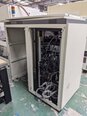
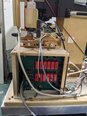
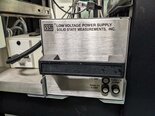
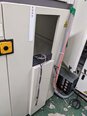
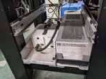
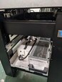
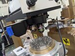
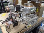
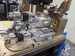
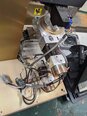
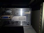
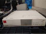
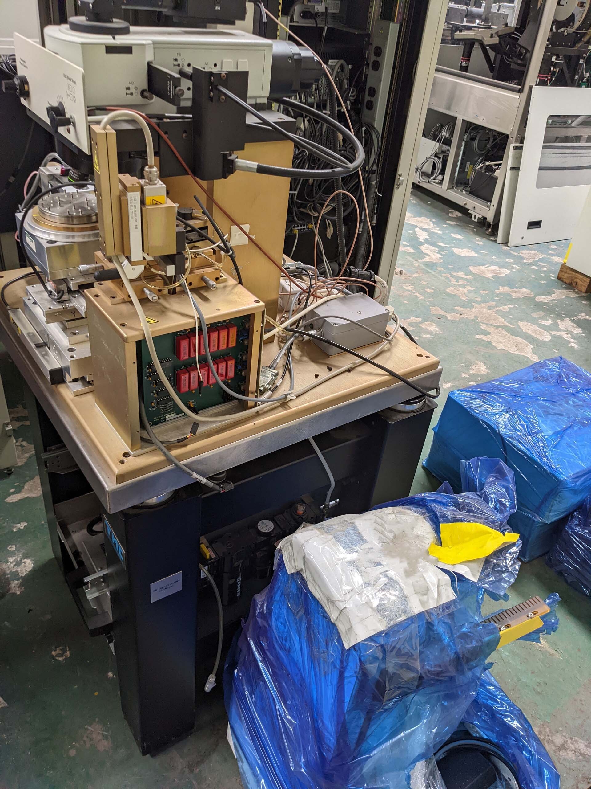
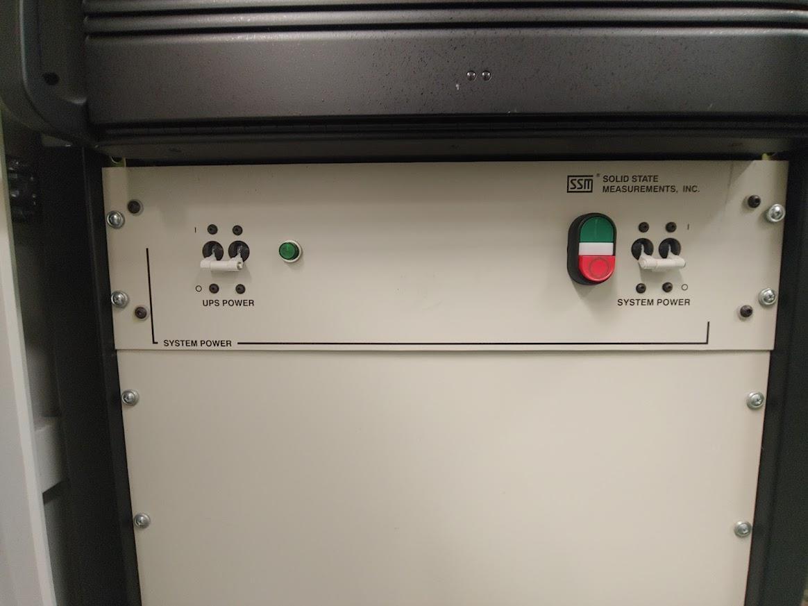
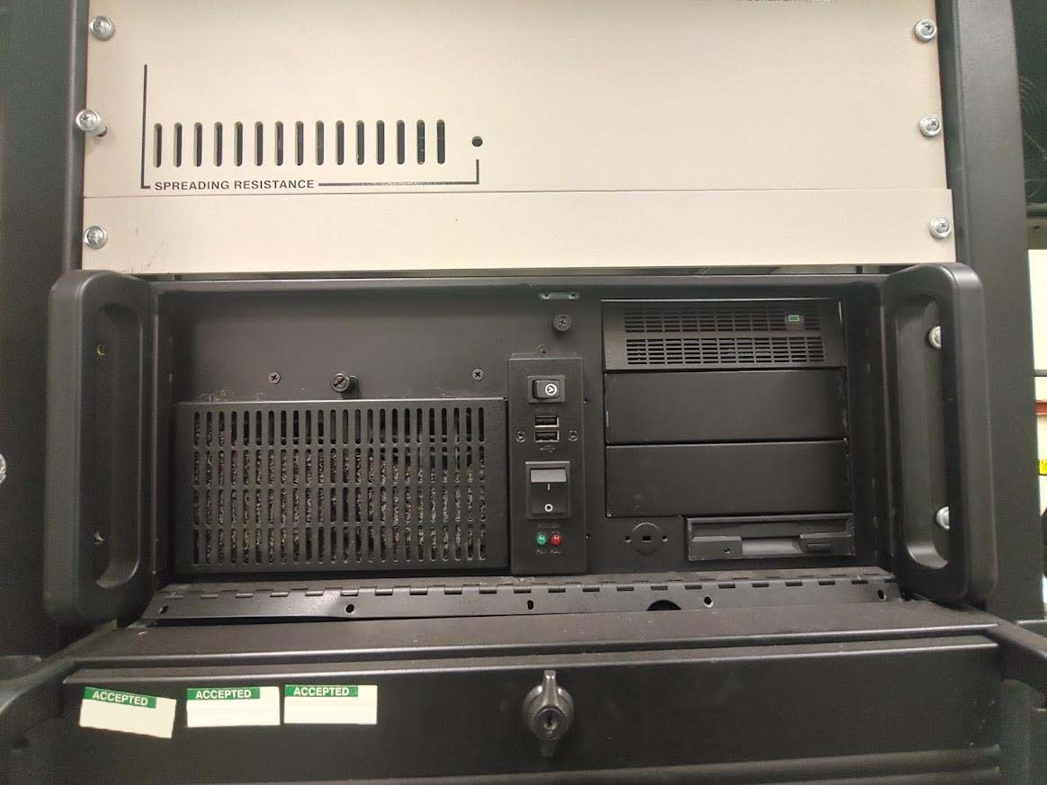
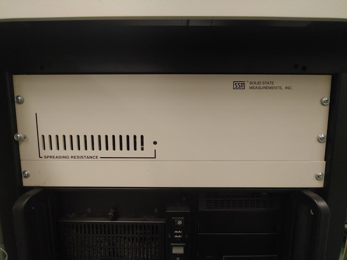
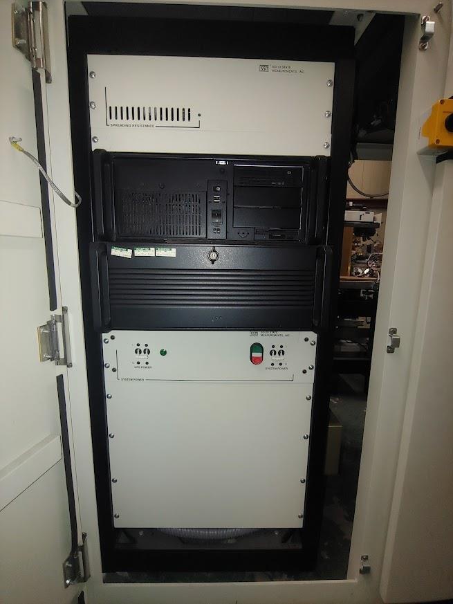
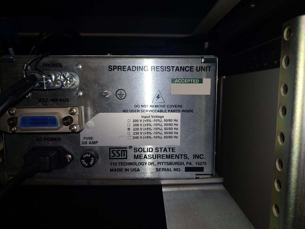
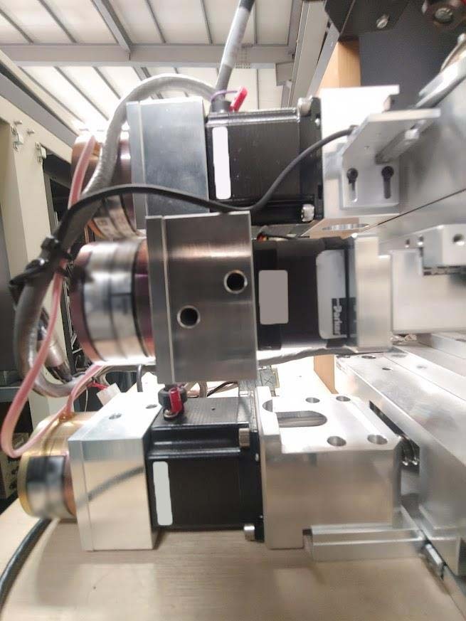
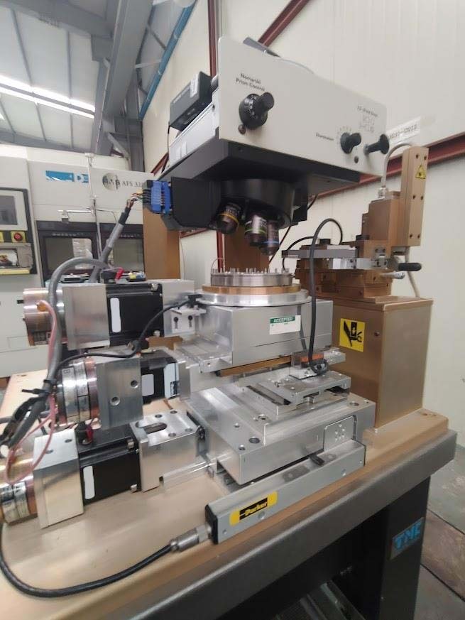
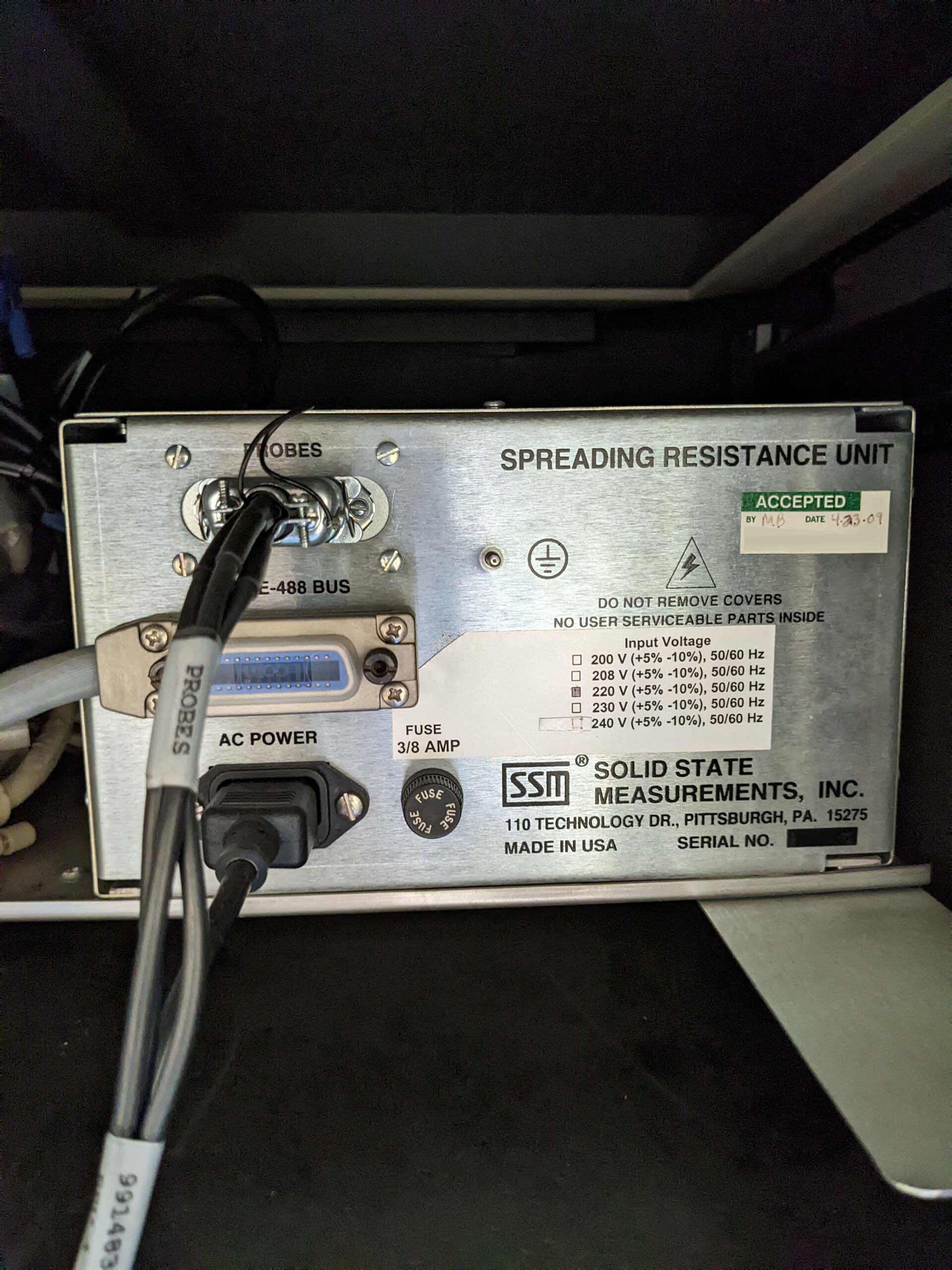
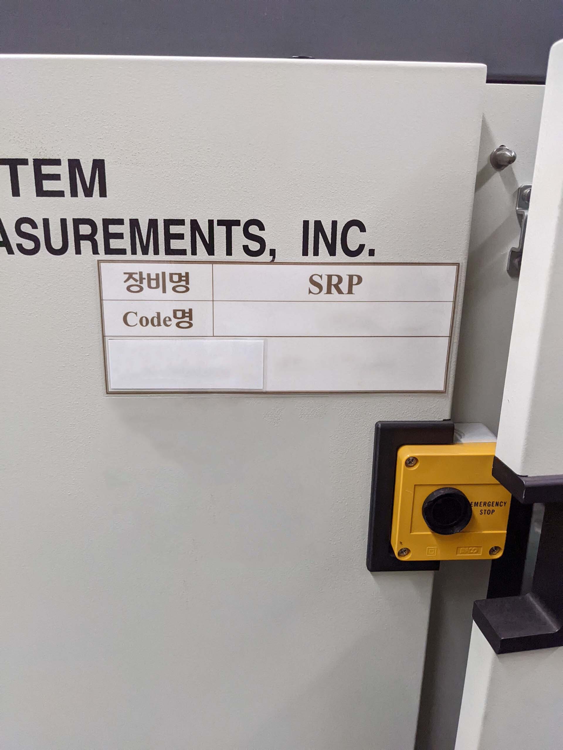
Spreading Resistance Profiling (SRP) system
2009 vintage.
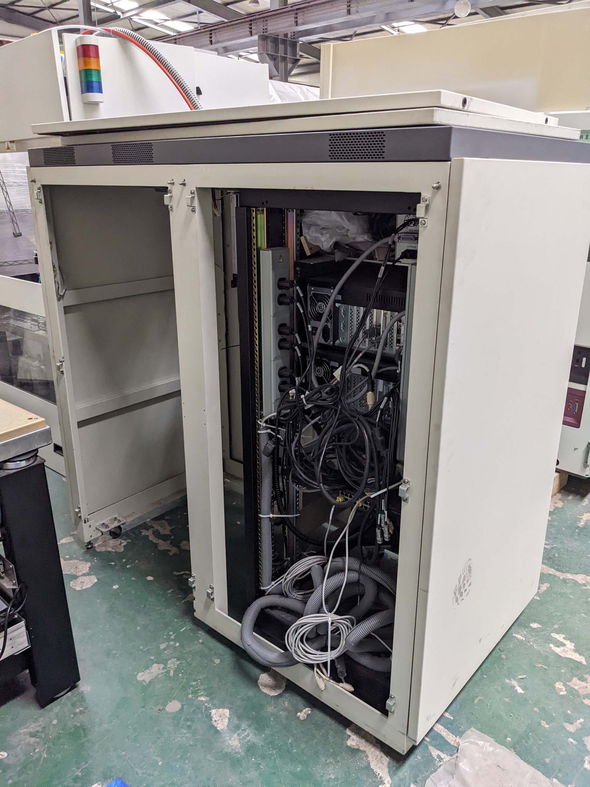
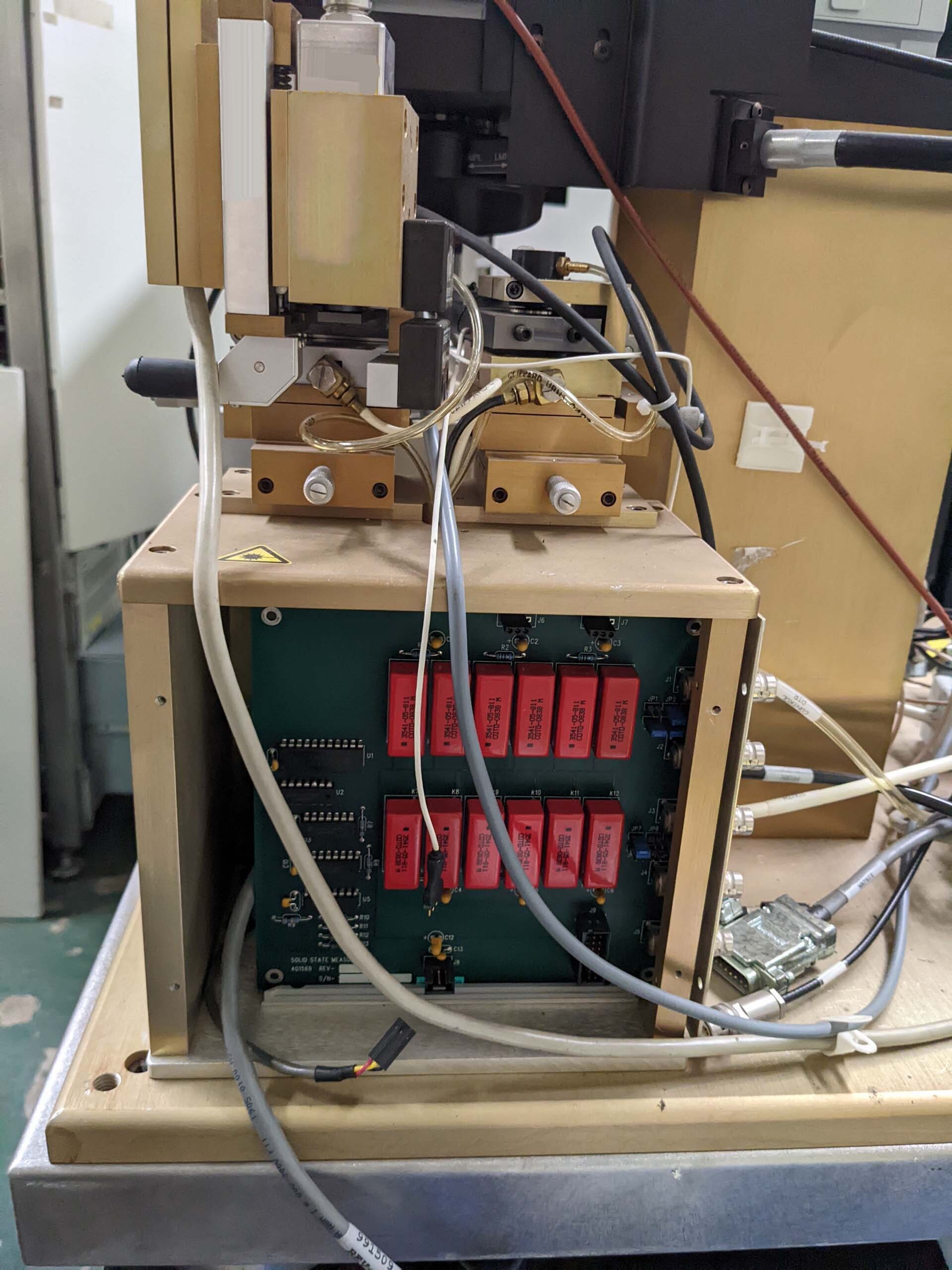
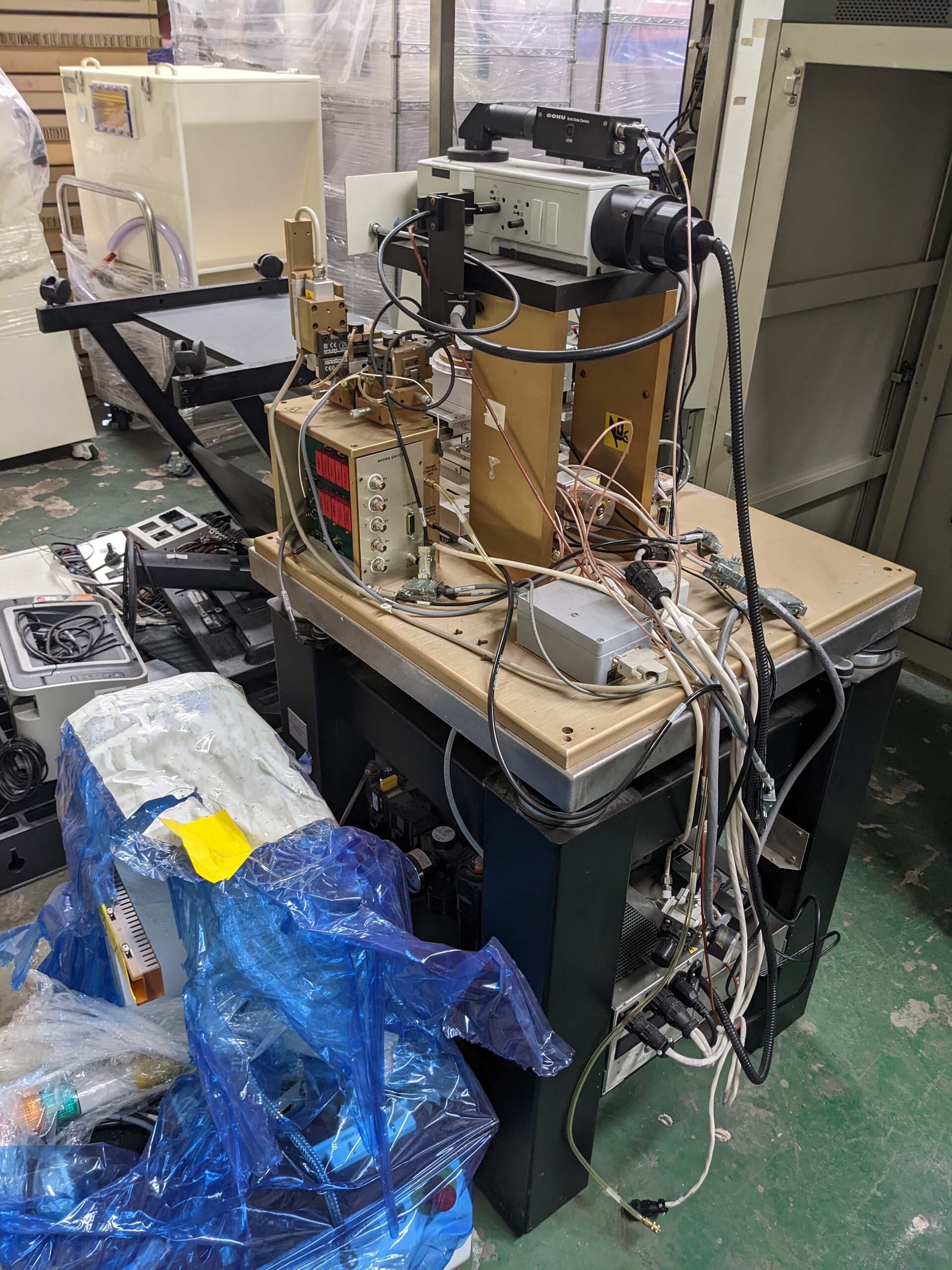
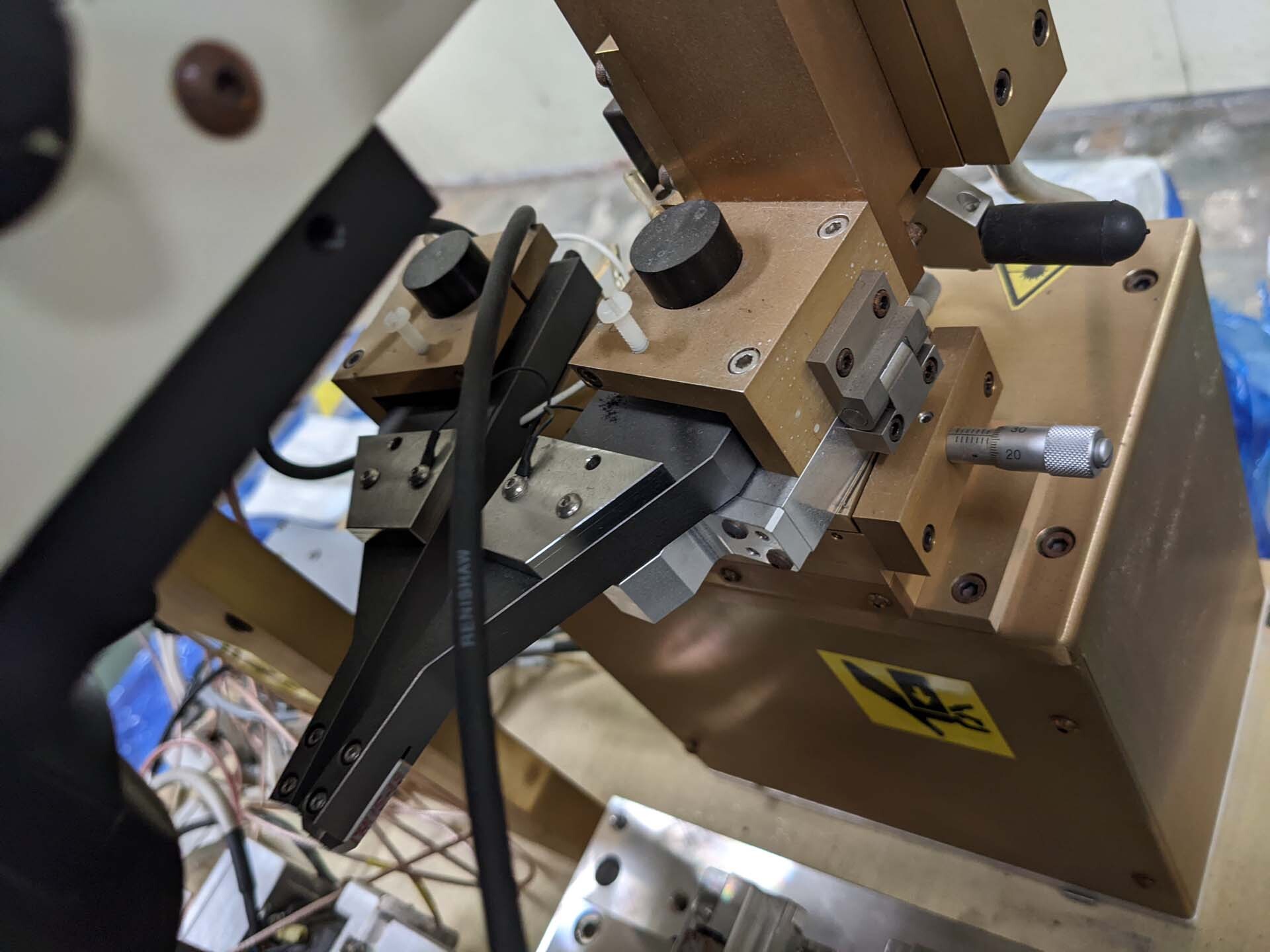
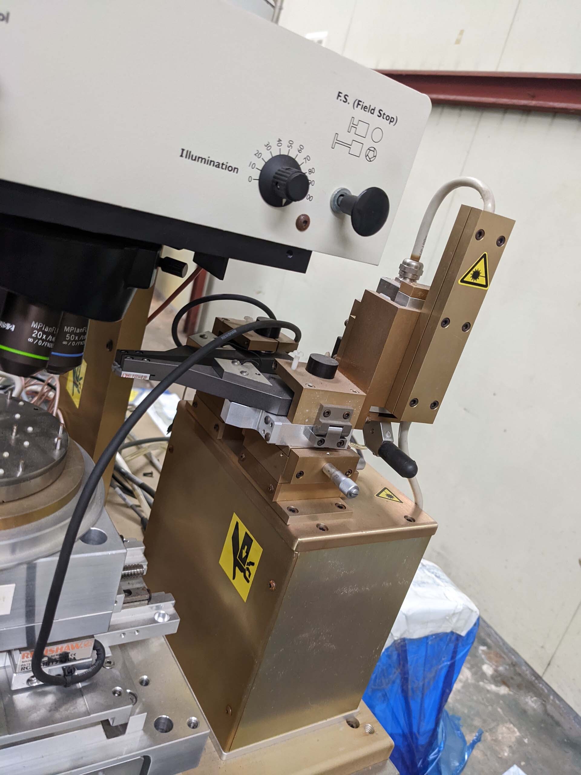
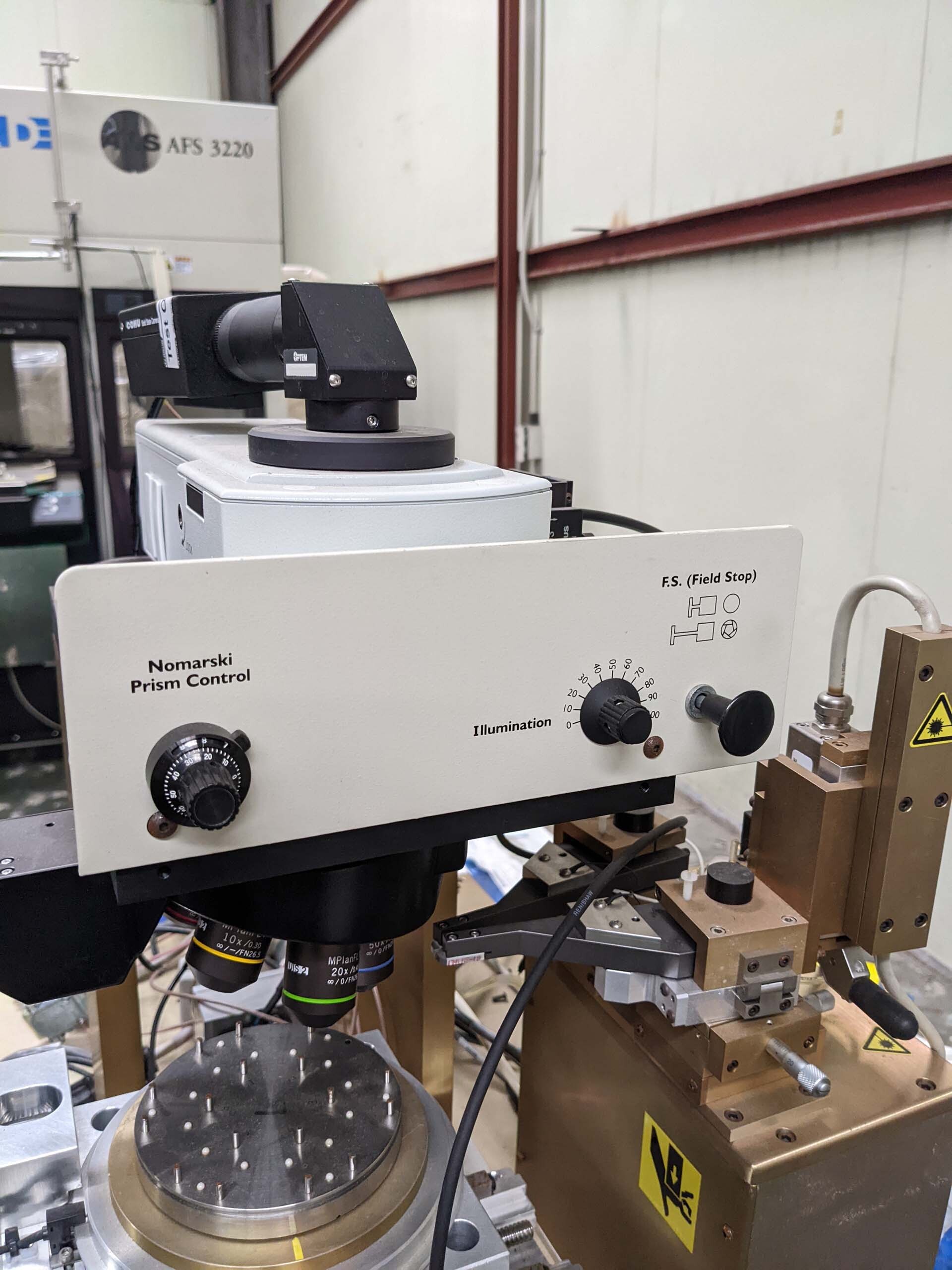
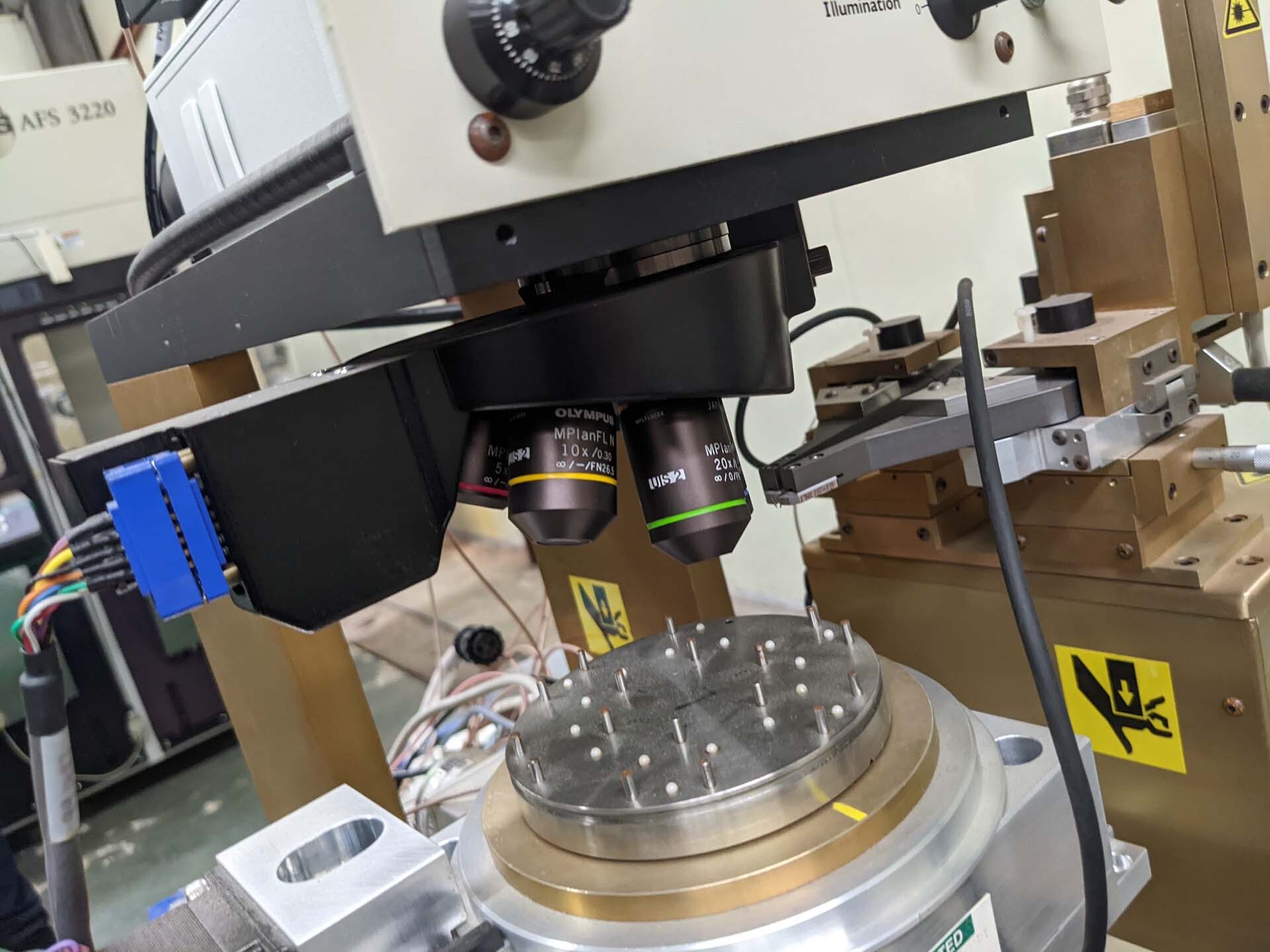
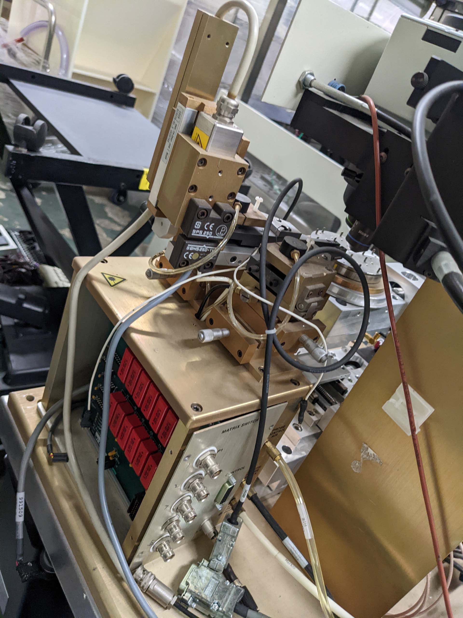
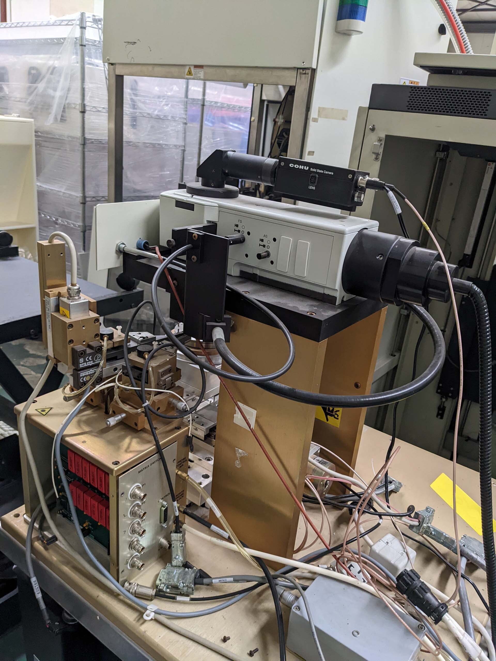
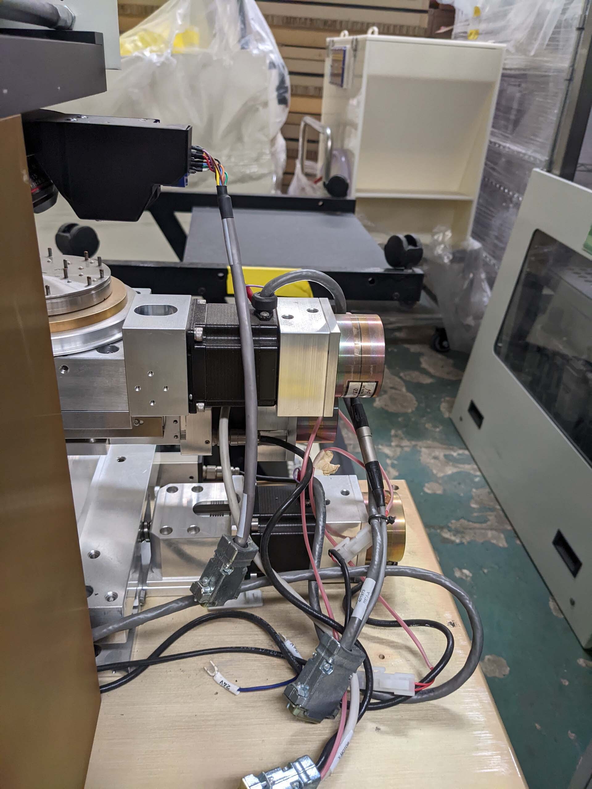
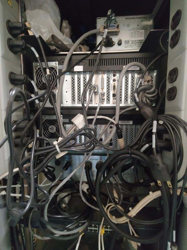
SEMILAB SSM2000 is a state-of-the-art wafer testing and metrology equipment designed for precise characterization of semiconductor materials and devices. This advanced system offers comprehensive capabilities for measuring key parameters such as dopant concentration, carrier mobility, stress/strain analysis, and defect detection on wafers with high accuracy and reliability. With its advanced technology and innovative features, SEMILAB SSM 2000 is an indispensable tool for semiconductor manufacturing and research applications. One of the key features of SSM2000 is its highly sensitive measurement capabilities. The unit utilizes advanced techniques such as capacitance-voltage (CV) and current-voltage (IV) measurements to accurately determine the electrical properties of semiconductor materials. By analyzing the CV and IV characteristics of the wafer, the machine can provide valuable insights into the doping profile, carrier concentration, and mobility of the semiconductor material, which are crucial parameters for optimizing device performance. In addition to electrical measurements, SSM 2000 is equipped with advanced optical and structural analysis capabilities. The tool can perform photoluminescence (PL) and Raman spectroscopy measurements to analyze the optical properties of the wafer, including bandgap energy, defect density, and crystal quality. By combining these optical measurements with structural analysis techniques such as scanning electron microscopy (SEM) and atomic force microscopy (AFM), the asset can provide a comprehensive characterization of the material's physical and chemical properties. SEMILAB SSM2000 also incorporates innovative stress/strain analysis capabilities to evaluate the mechanical properties of the wafer. By applying a controlled mechanical stress to the sample and measuring the resulting strain using techniques such as X-ray diffraction or Raman spectroscopy, the model can quantify the material's elastic modulus, residual stress, and strain distribution. This information is essential for optimizing the reliability and performance of semiconductor devices, especially in applications where mechanical stress plays a critical role. Another key feature of SEMILAB SSM 2000 is its defect detection capability. The equipment can perform non-destructive testing using techniques such as infrared thermography, ultrasound, and optical microscopy to identify and locate defects in the wafer, including cracks, voids, and process-induced anomalies. By precisely mapping the defects on the wafer surface and correlating them with electrical and optical measurements, the system can help manufacturers identify process issues and improve yield rates in semiconductor production. Overall, SSM2000 is a versatile and powerful wafer testing and metrology unit that offers comprehensive capabilities for characterizing semiconductor materials and devices. With its advanced measurement techniques, sensitive sensors, and innovative analysis features, the machine provides valuable insights into the electrical, optical, structural, and mechanical properties of wafers, helping manufacturers and researchers achieve higher device performance, reliability, and yield in semiconductor applications.
There are no reviews yet